

Philips SAA7705H Datasheet
INTEGRATED CIRCUITS
DATA SH EET
SAA7705H
Car radio Digital Signal Processor
(DSP)
Preliminary specification
File under Integrated Circuits, IC01
1999 Aug 16

Philips Semiconductors Preliminary specification
Car radio Digital Signal Processor (DSP) SAA7705H
CONTENTS
1 FEATURES
1.1 Hardware
1.2 Software
2 APPLICATIONS
3 GENERAL DESCRIPTION
4 QUICK REFERENCE DATA
5 ORDERING INFORMATION
6 BLOCK DIAGRAM
7 PINNING
8 FUNCTIONAL DESCRIPTION
8.1 FM and level information processing
8.1.1 Signal path for level information
8.1.2 Signal path from FMMPX input to IAC and
stereo decoder
8.1.3 Input sensitivity for FM and RDS signals
8.1.4 AD input selection switch
8.1.5 Interference absorption circuit
8.2 Analog source selection and analog-to-digital
conversion
8.2.1 Input selection switches
8.2.2 Signal flow of the AM, analog CD and TAPE
inputs
8.2.3 The analog CD block
8.2.4 Pin VREFAD
8.2.5 Pins VDACN1, VDACN2 and VDACP
8.2.6 Supply of the analog inputs
8.3 Analog outputs
8.3.1 DACs
8.3.2 Upsample filter
8.3.3 Volume control
8.3.4 Function of pin POM
8.3.5 Power-off plop suppression
8.3.6 The internal pin VREFDA
8.3.7 Internal DAC current reference
8.3.8 Supply of the analog outputs
8.4 Clock circuit and oscillator
8.4.1 Supply of the crystal oscillator
8.4.2 The phase-locked loop circuit to generate the
DSP clock and other derived clocks
8.4.3 The clock block
8.4.4 Synchronization with the core
8.5 Equalizer accelerator circuit
8.5.1 Introduction
8.5.2 EQ circuit overview
8.5.3 Controller and programming circuit
8.6 The DSP core
8.7 External control pins and status register
8.8 I2C-bus interface (pins SCL and SDA)
8.9 I2S-bus inputs and outputs
8.10 RDS decoder (pins RDSCLK and RDSDAT)
8.10.1 Clock and data recovery
8.10.2 Timing of clock and data signals
8.10.3 Buffering of RDS data
8.10.4 Buffer interface
8.11 DSP reset
9 LIMITING VALUES
10 THERMAL CHARACTERISTICS
11 CHARACTERISTICS
12 I2C-BUS INTERFACE AND PROGRAMMING
12.1 I2C-bus interface
12.1.1 Characteristics of the I2C-bus
12.1.2 Bit transfer
12.1.3 Start and stop conditions
12.1.4 Data transfer
12.1.5 Acknowledge
12.2 I2C-bus protocol
12.2.1 Addressing
12.2.2 Slave address
12.2.3 Write cycles
12.2.4 Read cycles
12.3 Memory map specification and register
overview
12.4 Register description
12.5 Detailed register description
13 APPLICATION INFORMATION
13.1 Software description
13.2 Power supply connection and EMC
14 PACKAGE OUTLINE
15 SOLDERING
15.1 Introduction to soldering surface mount
packages
15.2 Reflow soldering
15.3 Wave soldering
15.4 Manual soldering
15.5 Suitability of surface mount IC packages for
wave and reflow soldering methods
16 DEFINITIONS
17 LIFE SUPPORT APPLICATIONS
18 PURCHASE OF PHILIPS I2C COMPONENTS
1999 Aug 16 2

Philips Semiconductors Preliminary specification
Car radio Digital Signal Processor (DSP) SAA7705H
1 FEATURES
1.1 Hardware
• Three 3rd-order Switched Capacitor Analog-to-Digital
converters (SCADs)
• Digital-to-Analog Converters (DACs) with four times
oversampling and noise shaping
• Digital stereo decoder for the FM multiplex signal
• ImproveddigitalInterferenceAbsorptionCircuit(IAC)for
FM
• Radio Data System (RDS) processing with an optional
16-bit buffer via a separate channel (two tuners
possible)
• Auxiliary high Common-Mode Rejection Ratio (CMRR)
analog CD input (CD-walkman, speech, economic
CD-changer, etc.)
• I2C-bus controlled
• Four channel 5-band I2C-bus controlled parametric
equalizer
• Twoseparate full I2S-busand LSB-justified formats high
performance input interfaces
• Audio output short-circuit protected
• Separate AM left and right inputs
• Phase-Locked Loop (PLL) to generate the high
frequency DSP clock from a common fundamental
oscillator crystal
• Analog single-ended tape inputs
• I2S-bus subwoofer output (mono or stereo)
• Expandable with additional DSPs for sophisticated
features through an I2S-bus gateway
• Operating ambient temperature from −40 to +85 °C.
1.2 Software
• Improved FM weak signal processing
• Integrated 19 kHz MPX filter and de-emphasis
• Electronic adjustments: FM/AM level, FM channel
separation and Dolby level
• Baseband audio processing (treble, bass, balance,
fader and volume)
• Dynamic loudness or bass boost
• Audio level meter
• Tape equalisation (tape analog playback)
• Music Search System (MSS) detection for tape
• Dolby-B tape noise reduction
• Adjustable dynamics compressor
• CD de-emphasis processing
• Improved AM reception
• Soft audio mute
• AM IAC
• Pause detection for RDS updates
• Signal level, noise and multipath detection for AM/FM
signal quality information.
2 APPLICATIONS
• Car radio systems.
3 GENERAL DESCRIPTION
The SAA7705H performs all the signal functions in frontof
the power amplifiers and behind the AM and FM multiplex
demodulation of a car radio or the tape input.
These functions are:
• Interference absorption
• Stereo decoding
• RDS decoding
• FM and AM weak signal processing (soft mute, sliding
stereo, etc.)
• Dolby-B tape noise reduction
• Audio controls (volume, balance, fader and tone).
Some functions have been implemented in the hardware
(stereo decoder, RDS decoding and IACfor FM multiplex)
and are not freely programmable. Digital audio signals
fromexternalsourceswith the Philips I2S-busformatorthe
LSB-justified 16, 18 or 20 bits format are accepted.
There are four independent analog output channels.
The channels have a hardware implemented 5-band
parametric equalizer, controlled via the I2C-bus.
1999 Aug 16 3
Philips Semiconductors Preliminary specification
Car radio Digital Signal Processor (DSP) SAA7705H
The DSP contains a basic program that enables aset with:
• AM/FM reception
• Sophisticated FM weak signal functions
• Music Search System (MSS) detection for tape
• Dolby-B tape noise reduction system
• CD play with compressor function
• Separate bass and treble tone control and fader or
balance control additional to the equalizers.
4 QUICK REFERENCE DATA
SYMBOL PARAMETER CONDITIONS MIN. TYP. MAX. UNIT
Supply
V
DDD3V
digital supply voltage
V
DDD3Vx
pins with respect to VSS3 3.3 3.6 V
3.3 V for DSP core
I
DDD3V
V
DDD5V
supply current of the
3.3 V digital DSP core
supply voltage 5 V for
high activity of the DSP at
27 MHz DSP frequency
V
pins with respect to VSS4.5 5 5.5 V
DDDV5x
− 80 110 mA
periphery
I
DDD5V
supply current of the 5 V
− 35mA
digital periphery
V
DDA
analog supply voltage
V
pins with respect to V
DDAx
3 3.3 3.6 V
SS
3.3 V
I
DDA
Analog level inputs (AML and FML); T
S/N
LAD
analog supply current zero input and output signal − 40 50 mA
level-ADCsignal-to-noise
ratio
=25°C; V
amb
0 to 29 kHz bandwidth;
maximum input level;
= 3.3 V; unless otherwise specified
DDA1
48 54 − dB
unweighted
V
i(LAD)
input voltage level-ADC
0 − V
DDA1
for full-scale
Analog inputs; T
THD
FMMPX
=25°C; V
amb
= 3.3 V; unless otherwise specified
DDA1
total harmonic distortion
FMMPX input
input signal 0.35 V (RMS) at
1 kHz; bandwidth = 19 kHz;
−−70 −65 dB
− 0.03 0.056 %
note 1
S/N
FMMPX(m)
signal-to-noise ratio
FMMPX input mono
input signal at 1 kHz;
0 dB reference = 0.35 V (RMS);
80 83 − dB
bandwidth = 19 kHz; note 1
S/N
FMMPX(s)
signal-to-noise ratio
FMMPX input stereo
input signal at 1 kHz;
0 dB reference = 0.35 V (RMS);
74 77 − dB
bandwidth = 40 kHz; note 1
THD
CD
total harmonic distortion
CD inputs
input signal 0.55 V (RMS) at
1 kHz; input gain = 1;
−−83 −78 dB
− 0.007 0.013 %
bandwidth = 20 kHz
S/N
CD
signal-to-noise ratio CD
inputs
input signal at 1 kHz;
0 dB reference = 0.55 V (RMS);
81 84 − dB
bandwidth = 20 kHz
THD
AM
total harmonic distortion
AM inputs
input signal 0.55 V (RMS) at
1 kHz; bandwidth = 5 kHz
−−80 −76 dB
− 0.01 0.016 %
V
1999 Aug 16 4
Philips Semiconductors Preliminary specification
Car radio Digital Signal Processor (DSP) SAA7705H
SYMBOL PARAMETER CONDITIONS MIN. TYP. MAX. UNIT
S/N
AM
THD
TAPE
S/N
TAPE
V
i(con)(max)(rms)
Analog outputs; T
(THD + N)/S total harmonic
DR dynamic range output signal −60 dB at 1 kHz;
DS digital silence output signal at
Oscillator (f
f
xtal
f
clk(DSP)
signal-to-noise ratio AM
inputs
input signal at 1 kHz;
0 dB reference = 0.55 V (RMS);
83 88 − dB
bandwidth = 5 kHz
total harmonic distortion
TAPE inputs
signal-to-noise ratio
TAPE inputs
input signal 0.55 V (RMS) at
1 kHz; bandwidth = 20 kHz;
input signal at 1 kHz;
0 dB reference = 0.55 V (RMS);
−−80 −76 dB
− 0.01 0.016 %
81 83 − dB
bandwidth = 20 kHz
maximum conversion
THD < 1% 0.6 0.66 − V
input level at analog
inputs (RMS value)
=25°C; V
amb
distortion-plus-noise to
signal ratio
= 3.3 V; unless otherwise specified
DDA2
output signal 0.72 V (RMS) at
f = 1 kHz; R
>5kΩ (AC);
L
A-weighted
−−75 −65 dBA
92 102 − dBA
0 dB reference = 0.77 V (RMS);
A-weighted
−−108 −102 dBA
20 Hz to 17 kHz;
0 dB reference = 0.77 V (RMS);
A-weighted
= 11.2896 MHz)
osc
crystal frequency − 11.2896 − MHz
clock frequency
− 27.1656 − MHz
DSP core
Note
1. FMRDS and FMMPX input sensitivity setting ‘000’ (see Table 17).
5 ORDERING INFORMATION
TYPE
NUMBER
NAME DESCRIPTION VERSION
PACKAGE
SAA7705H QFP80 plastic quad flat package; 80 leads (lead length 1.95 mm);
body 14 × 20 × 2.8 mm
1999 Aug 16 5
SOT318-2
This text is here in white to force landscape pages to be rotated correctly when browsing through the pdf in the Acrobat reader.This text is here in
_white to force landscape pages to be rotated correctly when browsing through the pdf in the Acrobat reader.This text is here inThis text is here in
white to force landscape pages to be rotated correctly when browsing through the pdf in the Acrobat reader. white to force landscape pages to be ...
1999 Aug 16 6
SSD3V2
SSD3V1
DDD5V3
DDD5V2
DDD5V1
V
TP5
21
LEVEL-ADC
SCAD1
SCAD2
SCAD3
RDS
DECODER
60 59
RDSDAT
V
RDSCLK
V
SAA7705H
V
OSCILLATOR
63 64
DD(OSC)
V
V
IAC
OSCIN
VDACP
VDACN1
AML
FML
CDLB
CDLI
CDRB
CDRI
CDGND
VREFAD
AMAFL
AMAFR
TAPEL
TAPER
FMMPX
FMRDS
SELFR
DDA1
V
1
2
4
3
73
72
71
70
77
78
67
66
69
68
80
79
61
RTCB
INPUT
STAGE
ANALOG
SOURCE
SELECTOR
TSCAN
SHTCB
SSA1
V
VDACN2
18174543 44 2762 29
TP4
TP3
TP2
TP1
handbook, full pagewidth
SSD3V4
SSD3V3
V
V
V
SIGNAL
LEVEL
SIGNAL
QUALITY
OSCOUT
SSD5V2
SSD5V1
V
STEREO
DECODER
SS(OSC)
V
SSD5V3
V
CD1CL
CD1WS
DDD3V1
V
4836 4622757674
CD2DATA
CD1DATA
DDD3V3
DDD3V2
V
V
52 555147372354535049
DIGITAL
SOURCE
SELECTOR
24 26 56 4228 25
CD2WS
V
CD2CL
DDD3V4
DSPIN2
DSPIN1
EQUALIZER
DSP CORE
I2C-BUS INTERFACE
57 58652019
SCL
SDA
DSPOUT1
40 4138 39
QUAD
DIGITAL
TO
ANALOG
CONVERTER
(QDAC)
A0
DSPOUT2
V
11
V
10
POM
5
FLV
16
FLI
15
FRV
13
FRI
14
RLV
9
RLI
8
6
RRV
7
RRI
12
VREFDA
IISOUT1
34
IISOUT2
35
IISCLK
30
IISWS
33
IISIN1
31
IISIN2
32
MGM119
DSPRESET
DDA2
SSA2
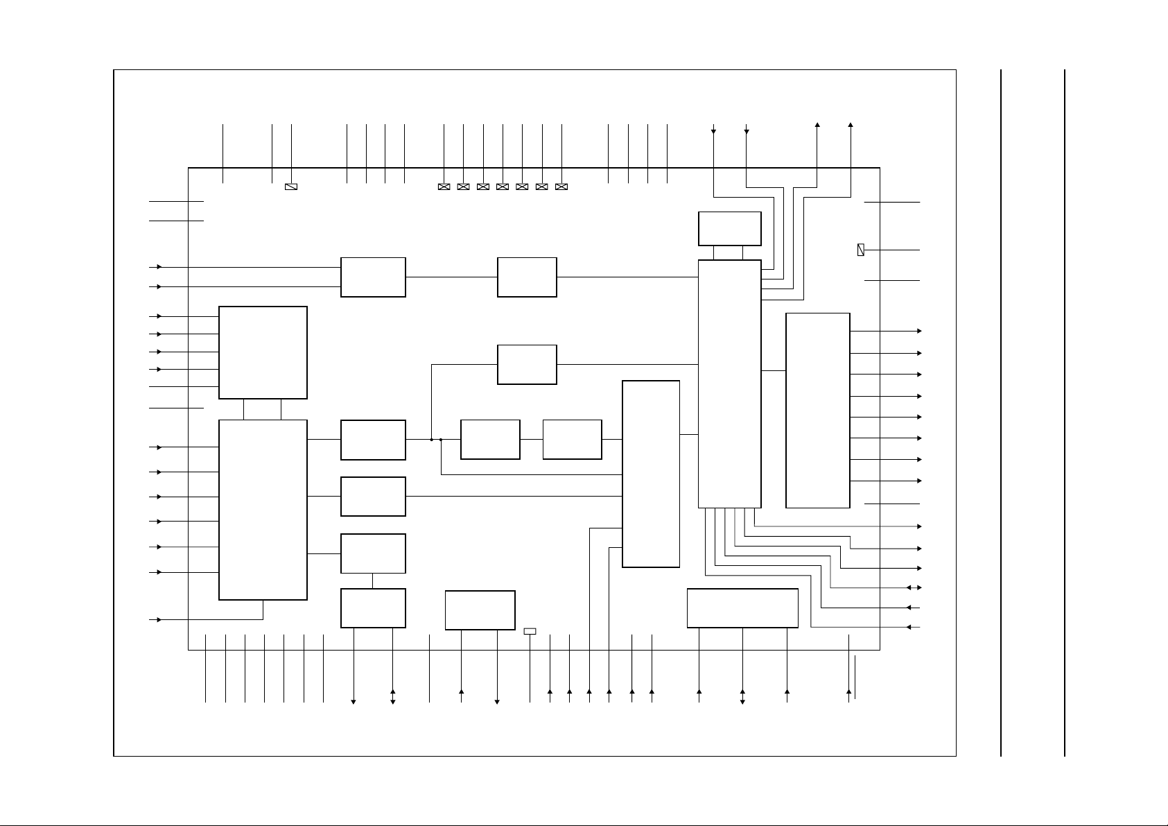
6 BLOCK DIAGRAM
Philips Semiconductors Preliminary specification
Car radio Digital Signal Processor (DSP) SAA7705H
Fig.1 Block diagram.

Philips Semiconductors Preliminary specification
Car radio Digital Signal Processor (DSP) SAA7705H
7 PINNING
SYMBOL PIN PIN TYPE DESCRIPTION
VDACP 1 AP2D positive reference voltage for SCAD1, SCAD2, SCAD3 and level-ADC
VDACN1 2 AP2D ground reference voltage 1 for SCAD1, SCAD2, SCAD3 and level-ADC
FML 3 AP2D FM level input; via this pin the level of the FM signal is fed to the SAA7705H; the
level information is needed for a correct functioning of the weak signal behaviour
AML 4 AP2D AM level input; via this pin the level of the AM signal is fed to the SAA7705H
POM 5 AP2D power-on mute of the QDAC; timing is determined by an external capacitor
RRV 6 AP2D rear right audio voltage output of the QDAC
RRI 7 AP2D rear right audio current output of the QDAC
RLI 8 AP2D rear left audio current output of the QDAC
RLV 9 AP2D rear left audio voltage output of the QDAC
V
SSA2
V
DDA2
VREFDA 12 AP2D decoupling for voltage reference of the analog part of the QDAC
FRV 13 AP2D front right audio voltage output of the QDAC
FRI 14 AP2D front right audio current output of the QDAC
FLI 15 AP2D front left audio current output of the QDAC
FLV 16 AP2D front left audio voltage output of the QDAC
TP1 17 BT4CR test pin, used in factory test mode, must not be connected
TP2 18 BT4CR test pin, used in factory test mode, must not be connected
TP3 19 BT4CR test pin, used in factory test mode, must not be connected
TP4 20 BT4CR test pin, used in factory test mode, must not be connected
TP5 21 IBUFD test pin, used in factory test mode, must be connected to V
V
DDD5V1
V
SSD5V1
CD2WS 24 IBUFD word select input 2 from a digital audio source (I2S-bus or LSB-justified format)
CD2DATA 25 IBUFD left or right data input 2 from a digital audio source (I2S-bus or LSB-justified format)
CD2CL 26 IBUFD clock input 2 from a digital audio source (I2S-bus or LSB-justified format)
CD1WS 27 IBUFD word select input 1 from a digital audio source (I2S-bus or LSB-justified format)
CD1DATA 28 IBUFD left or right data input 1 from a digital audio source (I2S-bus or LSB-justified format)
CD1CL 29 IBUFD clock input 1 from a digital audio source (I2S-bus or LSB-justified format)
IISCLK 30 BT4CR clock output to extra DSP chip (I2S-bus)
IISIN1 31 IBUFD data input channel 1 (front) from extra DSP chip (I2S-bus)
IISIN2 32 IBUFD data input channel 2 (rear) from extra DSP chip (I2S-bus)
IISWS 33 BD4CR word select input or output for extra DSP chip (I2S-bus)
IISOUT1 34 BD4CR data output to extra DSP chip (I2S-bus)
IISOUT2 35 BD4CR subwoofer output (I2S-bus)
V
DDD5V2
V
SSD5V2
DSPIN1 38 IBUFD digital input 1 of the DSP core (flag F0 of the status register)
DSPIN2 39 IBUFD digital input 2 of the DSP core (flag F1 of the status register)
10 APVSS ground supply for the analog part of the QDAC
11 APVDD positive supply for the analog part of the QDAC
DDD5V
22 VDDE5 positive supply 1 for peripheral cells
23 VSSE5 ground supply 1 for peripheral cells
36 VDDE5 positive supply 2 for peripheral cells
37 VSSE5 ground supply 2 for peripheral cells
1999 Aug 16 7
Philips Semiconductors Preliminary specification
Car radio Digital Signal Processor (DSP) SAA7705H
SYMBOL PIN PIN TYPE DESCRIPTION
DSPOUT1 40 B4CR digital output 1 of the DSP core (flag F2 of the status register)
DSPOUT2 41 B4CR digital output 2 of the DSP core (flag F3 of the status register)
DSPRESET 42 IBUFU reset input to the DSP core (active LOW)
RTCB 43 IBUFD asynchronous reset test control block, connect to ground
SHTCB 44 IBUFD shift clock test control block, connect to ground
TSCAN 45 IBUFD scan control (active HIGH), connect to ground
V
DDD5V3
V
SSD5V3
V
DDD3V1
V
SSD3V1
V
SSD3V2
V
DDD3V2
V
DDD3V3
V
SSD3V3
V
SSD3V4
V
DDD3V4
A0 56 IBUFD I2C-bus address selection
SCL 57 SCHMITCD serial clock input (I2C-bus)
SDA 58 BD4SCI4 serial data input/output (I2C-bus)
RDSCLK 59 BD4CR RDS bit clock output or RDS external clock input
RDSDAT 60 BT4CR RDS data output
SELFR 61 IBUFD AD input selection switch; to enable high-ohmic FMMPX input at fast tuner search
V
SS(OSC)
OSCIN 63 AP2D crystal oscillator input: crystal oscillator sense for gain control or forced input in
OSCOUT 64 AP2D crystal oscillator output: drive output to 11.2896 MHz crystal
V
DD(OSC)
AMAFR 66 AP2D AM audio frequency analog input (right channel)
AMAFL 67 AP2D AM audio frequency analog input (left channel)
TAPER 68 AP2D tape analog input (right channel)
TAPEL 69 AP2D tape analog input (left channel)
CDRI 70 AP2D CD analog input (right channel)
CDRB 71 AP2D feedback input of the CD analog input (right channel)
CDLI 72 AP2D CD analog input (left channel)
CDLB 73 AP2D feedback input of the CD analog input (left channel)
V
DDA1
V
SSA1
VDACN2 76 AP2D ground reference voltage 2 for SCAD1, SCAD2, SCAD3 and level-ADC
46 VDDE5 positive supply 3 for peripheral cells
47 VSSE5 ground supply 3 for peripheral cells
48 VDDI3 positive supply 1 for DSP core
49 VSSI3 ground supply 1 for DSP core
50 VSSI3 ground supply 2 for DSP core
51 VDDI3 positive supply 2 for DSP core
52 VDDI3 positive supply 3 for DSP core
53 VSSI3 ground supply 3 for DSP core
54 VSSI3 ground supply 4 for DSP core
55 VDDI3 positive supply 4 for DSP core
on pin FMRDS; if SELFR is HIGH, the input at pin FMRDS is put through to SCAD1
and FMRDS gets high-ohmic; this pin works together with the AD register bit
SELTWOTUN (see Table 9)
62 APVSS ground supply for crystal oscillator circuit
slave mode
65 APVDD positive supply for crystal oscillator circuit
74 APVDD analog positive supply for SCAD1, SCAD2, SCAD3 and level-ADC
75 APVSS analog ground supply SCAD1, SCAD2, SCAD3 and level-ADC
1999 Aug 16 8
Philips Semiconductors Preliminary specification
Car radio Digital Signal Processor (DSP) SAA7705H
SYMBOL PIN PIN TYPE DESCRIPTION
CDGND 77 AP2D positive reference for analog CD block
VREFAD 78 AP2D common-mode reference voltage SCAD1, SCAD2, SCAD3 and level-ADC
FMRDS 79 AP2D FM RDS analog input
FMMPX 80 AP2D FM multiplex analog input
Table 1 Explanation of pin types
PIN TYPE DESCRIPTION
AP2D analog input/output
APVDD analog supply
APVSS analog ground
VDDE5 5 V peripheral supply
VSSE5 5 V peripheral ground connection, no connection to the substrate
VDDI3 3.3 V supply to digital core and internal I/O pads
VSSI3 3.3 V ground to digital core and internal I/O pads, no connection to the substrate
SCHMITCD CMOS, Schmitt trigger input with active pull-down
IBUFU CMOS, active pull-up to all VDDE5 pads
IBUFD CMOS, active pull-down to all VSSE5 pads
BD4CR bidirectional CMOS I/O buffer, 4 mA, slew rate control
BT4CR 4 mA CMOS 3-state output buffer, slew rate control
B4CR 4 mA CMOS output buffer, slew rate control
BD4SCI4 CMOS I/O pad with open-drain output
1999 Aug 16 9
Philips Semiconductors Preliminary specification
Car radio Digital Signal Processor (DSP) SAA7705H
handbook, full pagewidth
SSA1
VDACP
VDACN1
POM
RRV
V
SSA2
V
DDA2
VREFDA
V
DDD5V1
V
SSD5V1
CD2WS
FML
AML
RRI
RLI
RLV
FRV
FRI
FLI
FLV
TP1
TP2
TP3
TP4
TP5
CDGND
77
VDACN2
76
FMMPX
FMRDS
VREFAD
80
79
78
1
2
3
4
5
6
7
8
9
10
11
12
13
14
15
16
17
18
19
20
21
22
23
24
V
75
DDA1
V
CDLB
74
73
SAA7705H
CDLI
72
CDRB
71
CDRI
70
TAPEL
69
TAPER
68
AMAFL
67
AMAFR
V
66
DD(OSC)
65
64
63
62
61
60
59
58
57
56
55
54
53
52
51
50
49
48
47
46
45
44
43
42
41
OSCOUT
OSCIN
V
SS(OSC)
SELFR
RDSDAT
RDSCLK
SDA
SCL
A0
V
DDD3V4
V
SSD3V4
V
SSD3V3
V
DDD3V3
V
DDD3V2
V
SSD3V2
V
SSD3V1
V
DDD3V1
V
SSD5V3
V
DDD5V3
TSCAN
SHTCB
RTCB
DSPRESET
DSPOUT2
25
26
27
28
29
30
31
32
IISIN1
CD2CL
CD2DATA
CD1WS
CD1DATA
CD1CL
IISCLK
IISIN2
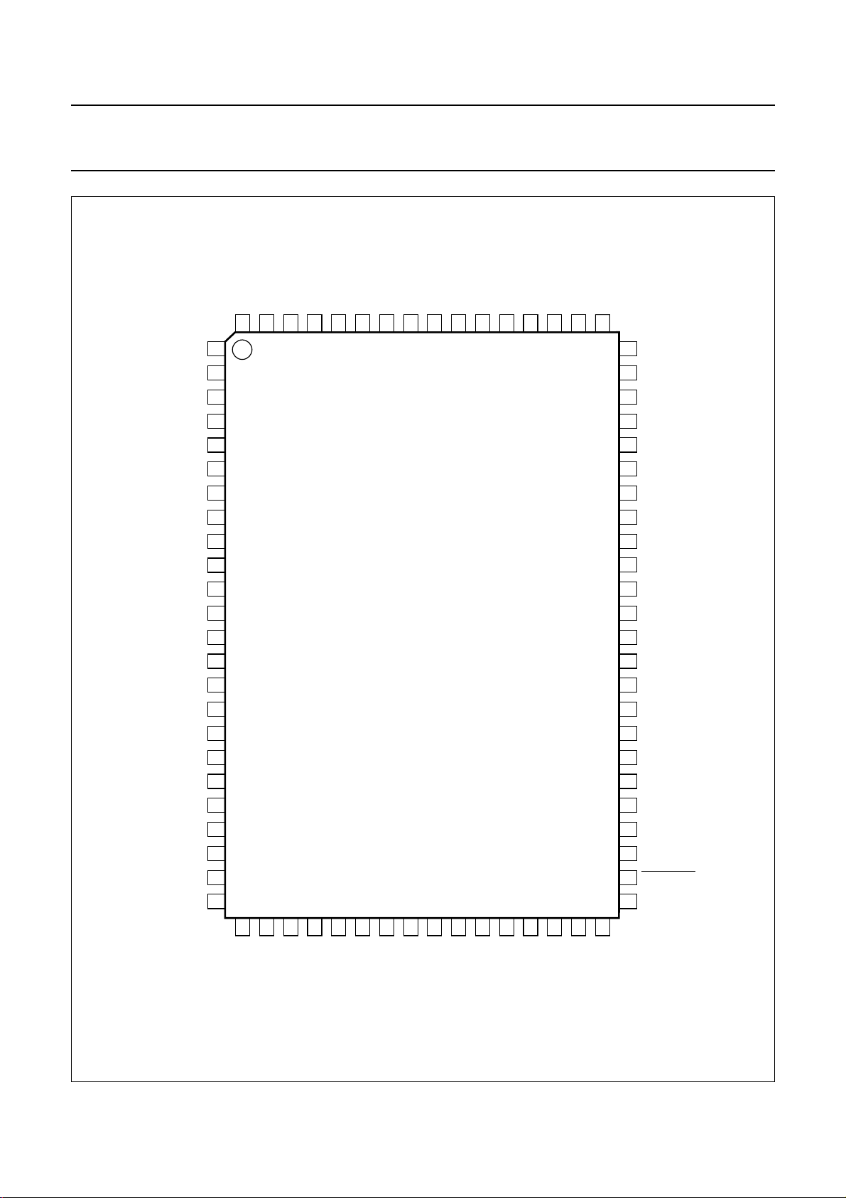
Fig.2 Pin configuration.
1999 Aug 16 10
33
IISWS
34
35
IISOUT1
IISOUT2
36
DDD5V2
V
V
37
38
DSPIN1
SSD5V2
39
40
DSPIN2
DSPOUT1
MGM118

Philips Semiconductors Preliminary specification
Car radio Digital Signal Processor (DSP) SAA7705H
8 FUNCTIONAL DESCRIPTION
The SAA7705H consists of a DSP core and periphery.
The DSP core is described in Sections 8.6, 8.7 and 8.11.
The periphery handles the following tasks:
• FM and level information processing (see Section 8.1)
• Analog source selection and analog-to-digital
conversion of the analog audio sources (see
Section 8.2)
• Digital-to-analog conversion of the DSP output QDAC
(see Section 8.3)
• Clock circuit and oscillator (see Section 8.4)
• Equalizer accelerator circuit (see Section 8.5)
• I2C-bus interface (see Section 8.8 and Chapter 12)
• RDS decoder (see Section 8.10).
8.1 FM and level information processing
8.1.1 SIGNAL PATH FOR LEVEL INFORMATION
For FM weak signal processing and for AM and FM
purposes (absolute level and multipath), an FM level and
an AM level input is implemented (pins FML and AML).
In the case ofradio reception clocking of the filters andthe
level-ADC is based on a 38 kHz sample frequency.
The DC input signal is converted by a bitstream first-order
Sigma-Delta ADC followed by a decimation filter.
The input signal has to be obtained from the radio part.
Two different configurations for AM and FM reception are
possible:
• Acircuitwith two separate level signals:oneforFM level
and one for AM level
• A combined circuit with AM and FM level information on
the FM level input.
The level input is selected with bit LEVAM-FM of the SEL
register (see Table 12 and Chapter 12).
8.1.2 SIGNAL PATH FROM FMMPX INPUT TO IAC AND
STEREO DECODER
The SAA7705H has four analog audio source channels.
One of the analog inputs is the FM multiplex signal.
Selection of this signal can be achieved by the SEL
register bits AUX-FM and CD-TAPE (see Table 12).
The multiplexed FM signal is converted to the digital
domain in SCAD1, a bitstream third-order SCAD. The first
decimation with a factor of 16 takes place in down sample
filter ADF1. This decimation filter can be switched by
means of the SEL register bit WIDE-NARROW
(see Table 12)in the wide ornarrowband position. In case
of FM reception, it must be in the narrow position.
The FMMPX path is followed by the sample-and-hold
switch of the IAC (see Section 8.1.5) and the 19 kHz pilot
signal regeneration circuit. A second decimation filter
reduces the output of the IAC to a lower sample rate.
One of the two filter outputs contains the multiplexed
signal with a frequency range of 0 to 60 kHz.
The outputs of this signal path to the DSP (which are all
running on a sample frequency of 38 kHz) are:
• Pilot presence indication: Pilot-I. This one bit signal is
LOW for a pilot frequency deviation <4 kHz and HIGH
for a pilot frequency deviation >4 kHz and locked on a
pilot tone.
• FM reception stereo signal. This is the 18-bit output of
the stereo decoder after the matrix decoding in
Information System Network (ISN) I2S-bus format.
This signal is fed via a multiplexer to a general I2S-bus
interface block that communicates with the DSP core.
• A noise level indication. This signal is derived from the
first MPX decimation filter via a wide band noise filter.
Detection is done with an envelope detector. This noise
level is filtered in the DSP core and is used to optimize
the FM weak signal processing.
8.1.3 INPUT SENSITIVITY FOR FM AND RDS SIGNALS
The FM and RDS input sensitivity is designed for tuner
front ends which deliver an output voltage varying from
65 to 225 mV (RMS) at a sweep of 22.5 kHz for a 1 kHz
tone. The intermediate standard input sensitivities can be
reached in steps of 1.6 dB, to be programmed with the
AD register bits VOLFM and VOLRDS (see Tables 9
and 17). The volume control of the FMMPX and the
FMRDS input can be controlled separately. VOLFM and
VOLRDS = 000is the most sensitive position,VOLFMand
VOLRDS = 111 the least sensitive position. Due to the
analog circuit control of the volume gain, the input
impedanceofpin FMMPX or pin FMRDS changes withthe
volume setting.
8.1.4 AD INPUT SELECTION SWITCH
Pin SELFR makes it possible to change to another
transmitter frequency with the same radio program to
assess the quality of that signal. In case of a stronger
transmitter signal the decision can be made by the
software to switch to the new transmitter. The FMMPX
input is normally used to process the FM signal.
This FMMPX input is connected via a relative large
capacitor to the MPX tuner output. Switching the tuner to
another transmitter frequency means another DC voltage
level on the MPX output of the tuner and a charging of the
1999 Aug 16 11
Philips Semiconductors Preliminary specification
Car radio Digital Signal Processor (DSP) SAA7705H
series capacitor (because the FMMPX input of the
SAA7705H is low-ohmic). Pulling SELFR HIGH during
such an update, causes the FMMPX input to become
high-ohmic, preventing charging of the capacitor.
The signal probing of the new transmitter quality is done
via the FMRDS input.
8.1.5 INTERFERENCE ABSORPTION CIRCUIT The Interference Absorption Circuit (IAC) detects and
suppresses ignition interference. This hardware IAC is a
modified, digitized and extended version of the analog
circuit which is in use for many years already.
The IAC consists of an MPX mute function switched by
mutepulses from two ignitioninterferencepulse detectors.
A third detector inhibits muting.
The three detectors are:
• Interference detector: The input signal of the first
detectoris the output signal ofSCAD1.Thisinterference
detector analyses the high frequency contents of the
MPX signal. The discrimination between interference
pulses and other signals is performed by a special
Philips patented fuzzy logic such as algorithm and is
based on probability calculations. This detector
performs optimally with higher antenna voltages.
On detection of ignition interference, this logic will send
appropriate pulses to the MPX mute switch.
• Level detector: The input signal of the second detector
is the FM level signal (the output of the level-ADC).
This detector performs optimally with lower antenna
voltages. It is therefore complementary to the first
detector.Thecharacteristicsofbothignitioninterference
pulse detectors can be adapted to the properties of
different FM front ends by means of the coefficients in
the IAC register and the level-IAC register
(see Section 12.4). Both IAC detectors can be switched
on or off independently. Both IAC detectors can mute
the MPX signal independently.
• Dynamic detector: The third detector is the dynamic
IAC circuit. This detector switches off the IAC
completelyif the frequency deviationof the FM multiplex
signal is too high. The use of narrow band IF filters can
result in AM modulation. This AM modulation could be
interpreted by the IAC circuitry as interference caused
by the car’s engine.
handbook, full pagewidth
FML 3
AML 4
AMAFR 66
TAPER 68
CDRB 71
CDRI 70
CDGND 77
AMAFL 67
TAPEL 69
CDLB 73
CDLI 72
FMMPX 80
FMRDS 79
SELFR 61
SELECTOR
ROUTER
GAIN
CONTROL
Fig.3 Analog input switching circuit.
LEVEL-ADC
SCAD2
INPUT
SCAD1
SCAD3
MGM123
1999 Aug 16 12

Philips Semiconductors Preliminary specification
Car radio Digital Signal Processor (DSP) SAA7705H
Parameter setting for the IAC detectors is done by means
of 5 different coefficients. Upon reset, the nominal setting
for a good performing IAC detector is selected.
8.1.5.1 AGC set point (1 bit)
In case the sensitivity and feed-forward factor are out of
range in a certain application, the set point of the AGC
can be shifted. The set point controls the sensitivity of
the other IAC control parameters. See bit 11 of the IAC
register (Table 11).
8.1.5.2 Threshold sensitivity offset (3 bits)
With this parameter the threshold sensitivity of the
comparator in the interfering pulse detectors can be set.
It also influences the amount of unwanted triggering.
Settings are according to Table 25.
8.1.5.3 Deviation feed-forward factor (3 bits)
This parameter determines the reduction of the sensitivity
of the detector by the absolute value of the MPX signal.
This mechanism prevents the detector from unwanted
triggering at noise with modulation peaks. In Table 24 the
possible values are given.
8.1.5.4 Suppression stretch time (3 bits)
This parameter sets the duration of the pulse suppression
after the detector has stopped sending a trigger pulse.
It can be switched off by setting the value ‘000’.
The duration can be selected in steps of one period of the
304 kHz (3.3 µs) sample frequency. In Table 23 the
possible values are given.
8.1.5.5 MPX delay (2 bits)
With this parameter the delay time between
2 and 5 samples of the 304 kHz sample frequency can be
selected. The needed value depends on the used front
end of the car radio. Settings are according to Table 22.
via the FMdemodulator and MPX conversion and filtering.
These differences depend on the front end used in the car
radio. With a simultaneous appearance of a peak
disturbance at the FM level input and the MPX ADC input
of the IC, a zero delay setting takes care for the level-IAC
mutepulse to coincidewiththe passage of thedisturbance
in the MPX mute circuit. The setting for the level-IAC
feed-forward allows to advance the mute pulse by
1 sample period or to delay it by 1 or 2 sample periods of
the 304 kHz clock, with respect to the default value.
The appropriate register bits for each setting are given in
Table 20.
8.1.5.8 Level-IAC suppression stretch time (2 bits)
This parameter sets the time that the mute pulse is
stretched when the FM level input has stopped exceeding
thethreshold. The durationcanbe selected insteps of one
period of the 304 kHz (3.3 µs) sample frequency.
In Table 19 the possible values are given.
8.1.5.9 Dynamic IAC threshold levels
If enabled by bit 15 of the LEVELIAC register, this block
will disable temporarily all IAC actions if the MPX mono
signal exceeds a threshold deviation (threshold 1) for a
given time with a given excess amount (threshold 2). This
MPX mono signal is separated from the MPX signal witha
low-pass filter with the −3 dB corner point at 15 kHz.
The possible values of this threshold are given in
Table 18.
8.1.5.10 IAC testing mode
The internal IAC trigger signal is visible on pin DSPOUT2
if bit IACTRIGGER of the IAC register is set. In this mode
the effect of the parameter settings on the IAC
performance can be verified.
8.2 Analog source selection and analog-to-digital
conversion
8.1.5.6 Level-IAC threshold (4 bits)
With this parameterthe sensitivity of the comparator in the
ignition interference pulse detector can be set. It also
influences the amount of unwanted triggering.
The possible values are given in Table 21. The prefix
value ‘0000’ switches off the level-IAC function.
8.1.5.7 Level-IAC feed-forward setting (2 bits)
This parameter allows for adjusting delay differences in
the signal paths from the FM antenna to the MPX mute,
namely, via the FM level-ADC andlevel-IAC detection and
1999 Aug 16 13
8.2.1 INPUT SELECTION SWITCHES
In Fig.3 the block diagram of the input is shown. The input
selection is controlled by bits in the input selector control
register and the input selection pin SELFR.
The relationship between these bits and the switches is
indicated in Table 26.
8.2.2 SIGNAL FLOW OF THE AM, ANALOG CD AND TAPE
INPUTS
The signal of the two single-ended stereo AM inputs can
be selected by the correct values of the SEL register bits
according to Table 26.

Philips Semiconductors Preliminary specification
Car radio Digital Signal Processor (DSP) SAA7705H
The AM and the TAPE inputs are buffered with an
operational amplifier to ensure a high-impedance input
which enables the use of an external resistor divider for
signal reduction. Forcorrect biasing of the first operational
amplifier a resistor must be connected between the input
and pin VREFAD, which acts as a virtual ground (see
Fig.21). The analog input switching circuit is shown in
Fig.3. The input for an analog CD player is explained in
more detail in Section 8.2.3.
8.2.3 THE ANALOG CD BLOCK Special precautions are taken to realize a high
Common-ModeRejectionRatio(CMRR) in case of theuse
of a CD player output processed via analog inputs.
The block diagram is shown in Fig.4. The operational
amplifiers OAR and OAL are used as buffers. The gain of
these operational amplifiers can be adjusted via the
externalresistors and is in thiscase 0.54by using a 8.2 kΩ
and a 15 kΩ resistor.
The reference inputs of these operational amplifiers are
connected to a separate pin CDGND. This pin is on one
side AC connected to the ground shielding of the cable
coming from the CD player and via a resistor >1 MΩ to
pin VREFAD. In this configuration the common-mode
signal propagates all the way to the SCAD block inputs of
SCAD1and SCAD2. TheSCADs themselves havea good
rejection ratio for in-phase common-mode signals.
Which part of the common-mode signal is processed as
the real input signal depends on the ratio of the
CDGND resistor and the series resistor in the cable and
the difference in input offset of the operational amplifiers.
The induced signals onthe CDLI andCDRI lines areof the
same amplitude and therefore rejected as common-mode
signals in the SCADs.
8.2.4 PIN VREFAD
The middle reference voltage of the SCAD1, SCAD2,
SCAD3 and level-ADC can be filtered via this pin.
This voltage is used as half the supply reference of the
SCAD1, SCAD2, SCAD3 and as the positive reference for
thelevel-ADC and buffers.Externalcapacitors (connected
to V
) prevent crosstalk between the SCADs and
SSA1
buffers and improve the power supply rejection ratio of all
blocks. This pin must also be used as a reference for the
inputs AMAFL, AMAFR, TAPEL, TAPER and CDGND.
8.2.5 PINS VDACN1, VDACN2 AND VDACP
These pins are used as ground and positive supply
reference for the SCAD1, SCAD2, SCAD3 and the
level-ADC. For optimal performance, pins VDACN1
and VDACN2 must bedirectly connected tothe V
pin VDACP to the filtered V
DDA1
.
SSA1
and
handbook, full pagewidth
CD-player
analog
output
LEFT
GROUND
RIGHT
15 kΩ
15 kΩ
8.2 kΩ
1 MΩ
8.2 kΩ
off-chip on-chip
Fig.4 Analog CD block.
1999 Aug 16 14
73CDLB
72CDLI
to SCAD2 via router
77CDGND
78VREFAD
71CDRB
70CDRI
OAL
to SCADs and level-ADC
to SCAD1 via router
OAR
MGM124
Philips Semiconductors Preliminary specification
Car radio Digital Signal Processor (DSP) SAA7705H
8.2.6 SUPPLY OF THE ANALOG INPUTS The analog input circuit has separate power supply
connections to allow maximum filtering of the analog
supply voltages: V
for the analog ground and V
SSA1
DDA1
for the analog supply.
8.3 Analog outputs
8.3.1 DACS Each of the four low noise high dynamic range DACs
consists of a 15-bit signed magnitude DAC with current
output, followed by a buffer operationalamplifier. For each
of the four audio output channels a separate convertor is
used. Each converter output is connected to the inverting
input of one of the four internal CMOS operational
amplifiers. The non-inverting input of this operational
amplifier is connected to the internal reference voltage.
Together with an internal resistor the conversion of
current-to-voltage of the audio output is achieved.
8.3.2 UPSAMPLE FILTER To reduce spectral components above the audio band, a
fixed 4 times oversampling and interpolating 18-bit digital
IIR filter is used. It is realized as a bit serial design and
consists of two consecutive filters. The data path in these
filters is 22 bits to prevent overflow and to maintain a
signal-to-noiseratio larger then 105 dB. Thewordclock for
theupsample filter (4 × fs)is derived fromthe audio source
timing. If the internal audio source is selected, the sample
frequencycan be either 44.1 or 38 kHz. Incaseofexternal
digital sources (CD1 and CD2), a sample frequency from
32 to 48 kHz is possible.
8.3.3 VOLUME CONTROL
Thetotalvolume control has adynamicrangeof more than
100 dB (0 dB being maximal input on the I2S-bus input).
With the signed magnitude noise shaped 15-bit DAC and
the internal 18-bit registers (these registers provide the
digital data communication between the DSP and the
QDAC) of the DSP core a useful digital volume control
range of 100 dB is possible by calculating the
corresponding coefficients.
The step size is freely programmable and an additional
analog volume control is not needed in this design.
The SNR of the audio output at full-scale is determined by
the total 15 bits of the converter. The noise at low outputs
is fully determined by the noise performance of the DAC.
Since it is a signed magnitude type, the noise at digital
silence is also low. The disadvantage is that the total THD
is higher than conventional DACs. The typical
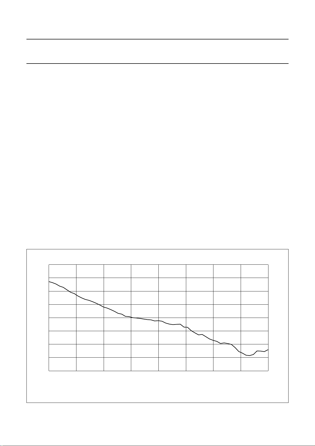
THD-plus-noise versus output level is shown in Fig.5.
handbook, full pagewidth
0
THD + N
(dB)
−20
−30
−40
−50
−60
−70
−80
−90
−80 −70
−40 0−30 −20 −10−60 −50
Fig.5 Typical THD + N curve versus output level.
1999 Aug 16 15
MGM125
output level (dB)

Philips Semiconductors Preliminary specification
Car radio Digital Signal Processor (DSP) SAA7705H
8.3.4 FUNCTION OF PIN POM
With pin POM it is possible to switch-off the reference
current of the DAC. The capacitor on pin POM
(see Fig.21) determines the time after which this current
has a soft switch-on. At power-on, the current audiosignal
outputs are always muted. The external capacitor is
loaded in two stages via two different current sources.
The loading starts at a current level that is 9 times lower
than the load current after the voltage on pin POM has
risen above 1 V. This results in an almost dB-linear
behaviour.However, the DAC hasanasymmetrical supply
and the DC output voltage will be half the supply voltage
under functional conditions. During start-up the output
voltage is not defined as long as the supply voltage is
below the threshold voltages of the transistors. A small
jump in DC is possible at start up. In this DC jump audio
components can be present.
8.3.5 POWER-OFF PLOP SUPPRESSION To avoid plops in a power amplifier, the supply voltage
(3.3 V)for the analog partof the DAC canbesupplied from
the 5 V supply via a transistor. A capacitor is connected to
V
to maintain power to the analog part if the 5 V
DDA2
supply is switched off fast. In this case the output voltage
will decrease gradually allowing the power amplifier some
extra time to switch-off without audible plops.
8.3.6 THE INTERNAL PIN VREFDA
8.3.8 SUPPLY OF THE ANALOG OUTPUTS
All the analog circuitry of the DACs and the operational
amplifiers are powered by 2 pins: V
DDA2
and V
SSA2.VDDA2
must have sufficient decoupling to prevent high THD and
to ensure a good Power Supply Rejection Ratio (PSRR).
The digital part of the DAC is fully supplied from the
DSP core supply.
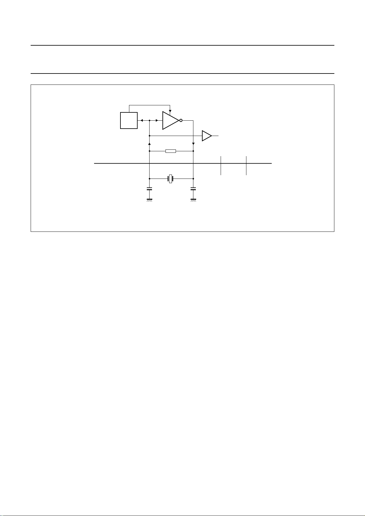
8.4 Clock circuit and oscillator
The device has an on-chip oscillator.The block diagramof
this Pierce oscillator is shown in Fig.6. The active element
neededtocompensateforthe loss resistance of the crystal
is the block Gm. This block is placed between the external
pins OSCIN and OSCOUT. The gain of the oscillator is
internally controlled by the AGC block. A sine wave with a
peak-to-peak voltage close to the oscillator power supply
voltage is generated. The AGC block prevents clipping of
the sine wave and therefore the generation of harmonics
as much as possible. At the same time the voltage of the
sine wave is as high as possible which reduces the jitter
going from the sine wave to the clock signal.
8.4.1 SUPPLY OF THE CRYSTAL OSCILLATOR
The supply of the oscillator is separated from the other
supplies. This minimizes the feedback from the ground
bounce of the chip to the oscillator circuit. Pin V
used as ground and pin V
DD(OSC)
as positive supply.
SS(OSC)
is
Using two internal resistors, half of the supply voltage
V
is obtained and coupled to an internal buffer.
DDA2
This reference voltage is used as a DC voltage for the
output operational amplifiers and as a reference for the
DAC. In order to obtain the lowest noise and to have the
best ripple rejection, a capacitor has to be connected
between this pin and ground.
8.3.7 INTERNAL DAC CURRENT REFERENCE Asa reference for theinternal DAC current andalsofor the
DAC current source output, a current is drawn from
pin VREFDA to V
(ground) via an internal resistor.
SSA2
The value of this resistor determines also the DAC current
(absolute value). Consequently, the absolute value of the
current varies from device to device due to the spread of
the reference resistor value. This, however, has no
influence on the absolute output voltages because these
voltages are derivedfrom a conversion of the DAC current
to the actual output voltage via internal resistors.
1999 Aug 16 16
8.4.2 THE PHASE-LOCKED LOOP CIRCUIT TO GENERATE
THE DSP CLOCK AND OTHER DERIVED CLOCKS
A PLL circuit is used to generate the DSP clock and other
derived clocks.
The minimum equalizer clock frequency is 480fs.
If fsequals 44.1 kHz, this results in a minimum oscillator
frequency of 21.1687 MHz. Crystals for the crystal
oscillator in the range of twice the required DSP clock
frequency (approximately 40 MHz) are always
third-overtone crystals and must be manufactured on
customer demand. This makes these crystals expensive.
The PLL enables the use of a commonly available crystal
operating in fundamental mode. For this circuit a
11.2896 MHz(256 × 44.1 kHz)crystalischosen.Thistype
of crystal is widely used.
Philips Semiconductors Preliminary specification
Car radio Digital Signal Processor (DSP) SAA7705H
handbook, full pagewidth
AGC
on-chip
off-chip
G
m
R
bias
63 64
OSCIN OSCOUT
Cx1
Fig.6 Block diagram of the oscillator circuit.
Although multiples of the crystal frequency of
11.2896 MHzfallwithin the FM reception band,thiswillnot
disturb the reception. The relatively low frequency crystal
is driven in a controlled way and the resonating crystal
produces harmonics of a very low amplitude in the FM
reception band.
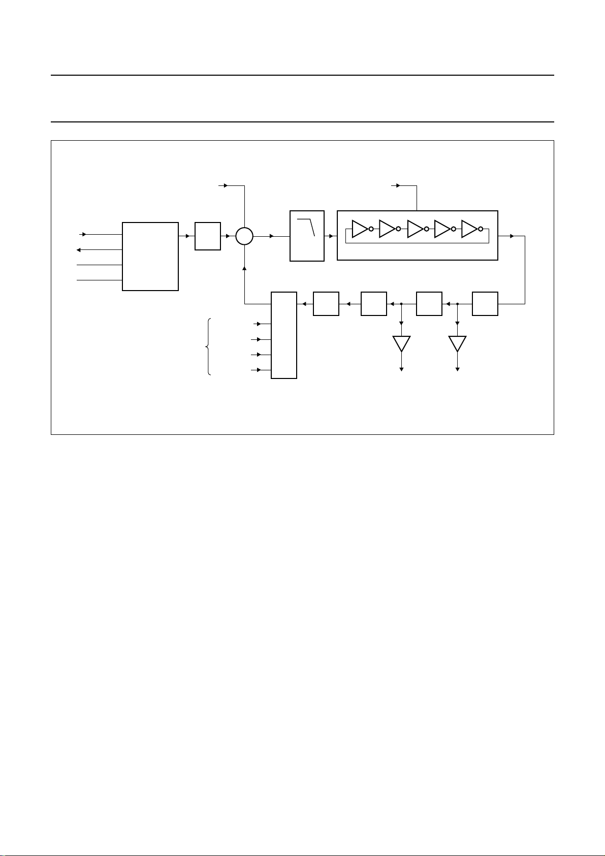
The block diagram of the programmable PLL is shown in
Fig.7. The oscillator is used in a fundamental mode.
The 11.2896 MHz oscillator frequency is divided by 256
and the resulting signal is fed to the phase detector as a
reference signal. The base for the clock signal is a current
controlled oscillator (free running frequency
70 to 130 MHz).
After having been divided by 4, the required clock
frequency for the DSP core is available. To close the loop
this signal is further divided by 4 and by the PLL clock
division factor N. N can be programmedwith the DCSCTR
register bits PLL-DIV (see Tables 7 and 15) in the range
from 93 to 181. This provides some flexibility in the choice
of the crystal frequency.
With the recommended crystal, N = 154 and the DSP
clockfrequency(f
)equals27.1656 MHz. N = 154 is the
DSP
default position at start-up. By setting the AD register bit
DSPTURBO (see Tables 9 and 15), the PLL output
frequency, and consequently f
, can be doubled.
DSP
This feature is not used in the proposed application.
clock to circuit
65 62
V
DD(OSC)VSS(OSC)
Cx2
MGM126
The clock frequency of the PLL oscillator divided by two
(2f
) is also used as the clock for the DCS block.
DSP
8.4.3 THE CLOCK BLOCK
For the digital stereo decoder a clock signal is needed
which is the 512-multiple of the pilot tone frequency of the
FMmultiplexsignal.This is done by the Digitally Controlled
Sampling (DCS) block, which generates this
512 × 19 kHz = 9.728 MHz clock, the DCS clock, by
locking to the pilot frequency. This block is also able to
generate other frequencies. It is controlled by the
DCSCTR and DCSDIV registers (see Tables 7 and 8).
Default settings of the DCS andthe PLL guaranteecorrect
functioning of the DCS block.
8.4.4 SYNCHRONIZATION WITH THE CORE
In case of I2S-bus input the system can run on audio
sample frequencies of fs= 32 kHz, 38 kHz, 44.1 kHz
or 48 kHz. After processing of an input sample, the Input
flag (I-flag) of the status register (see Section 8.7) of the
DSP core is set to logic 1 during 4 clock cycles on the
falling edge of the internal or external I2S-bus WS pulses.
This flag can be tested with a conditional branch
instruction in the DSP. This synchronisation starts in
parallelwith the input signal duetothe short period thatthe
I-flag is set. It is obvious that the higher fs the lower the
number of cycles available in the DSP program.
1999 Aug 16 17
Philips Semiconductors Preliminary specification
Car radio Digital Signal Processor (DSP) SAA7705H
I
handbook, full pagewidth
OSCIN
OSCOUT
V
DD(OSC)
V
SS(OSC)
OSCILLATOR
11.2896 MHz
from
DCSCTR
register
ref
44.1 kHz
÷256
PLL-DIV(0)
PLL-DIV(1)
PLL-DIV(2)
PLL-DIV(3)
×
PHASE
DETECTOR
÷N
Fig.7 Programmable PLL for DSP clock generation.
8.5 Equalizer accelerator circuit
8.5.1 INTRODUCTION The Equalizer accelerator (EQ) circuit is an equalizer
circuit used as a hardware accelerator to the DSP core.
Its inputs and outputs are stored in registers of the
DSP core (these registers provide the digital data
communication between the equalizer and the DSP core).
The flag that starts the DSP program, refreshes the EQ
input and output registers and starts the EQ controller.
The EQ circuit contains one second-order filter data path
that is twenty-fold multiplexed. With this circuit, a
two-channel equalizer of 10 second-order sections per
channel or a four-channel equalizer of 5 second-order
sections per channel can be realized.
The centre frequency, gain and Q-factor of all
20 second-order sections can be set independently from
each other. Every section is followed by a variable
attenuation of 0 or 6 dB. Per section, 4 bytes are needed
to store the settings. During an audio sample period, all
settings are read as 16-bit words in 80 read accesses to
the coefficient memory.
I
delay
70 to
130 MHz
LOOP
FILTER
N = 154
CURRENT CONTROLLED OSCILLATOR
÷2 ÷2÷2÷2
clock clock
27.1656 MHz 54.3312 MHz
MGM127
8.5.2 EQ CIRCUIT OVERVIEW
This EQ circuit contains the following parts:
• A second-order filter data path, with programmable
coefficients and with 40 state registers, supporting
storage of the two filter states for 20 multiplexed filters;
this part is clocked by a gated clock
• Signal routing around this filter data path, consisting of:
– busesand selectors to configurethe 20 filter sections
for two or four channels;
– inputandoutputregisters,withproperinterfacingwith
the DSP core and with conversions between parallel
and serial formats.
• A coefficient memory, to be loaded via the I2C-bus
interface
• A controller, started by the write pulse for input and
outputregisters, that controls thesignalrouting, controls
the clock for the filter data path, addresses the
coefficient memory and controls its programming.
1999 Aug 16 18
 Loading...