Philips SAA7500 Datasheet

INTEGRATED CIRCUITS
DATA SH EET
SAA7500
Digital satellite radio broadcasting
tuner decoder (SAT-2)
Product specification
File under Integrated Circuits, IC01
September 1989

Philips Semiconductors Product specification
Digital satellite radio broadcasting tuner
decoder (SAT-2)
GENERAL DESCRIPTION
The SAA7500 performs a decoder function for digital
satellite sound broadcasting tuners. It is designed to
decode one of 16 stereo channels broadcasting audio
signals in accordance with the German standard -
Technische Richtlinie ARD/ZDF Nr. 3R1.
Features
• Clock recovery
• Differential decoding
QUICK REFERENCE DATA
PARAMETER SYMBOL MIN. MAX. UNIT
Supply voltage V
Power dissipation P
Clock frequency T
DD
tot
20N
SAA7500
• Main frame synchronization
• Swapping half-frames in case of inversion
• Unscrambling
• Demultiplexing
• Subframe synchronization
• Error correction and concealment
• Scale factor decoding with error correction
• Shift into the original values using the scale factors
• Mute in case of synchronization loss
4.5 5.5 V
500 mW
20.48 MHz
PACKAGE OUTLINE
68-lead plastic leaded chip carrier (PLCC); ‘pocket’ version (SOT188AA); SOT188-2; 1996 September 05.
September 1989 2

Philips Semiconductors Product specification
Digital satellite radio broadcasting tuner
decoder (SAT-2)
SAA7500
September 1989 3
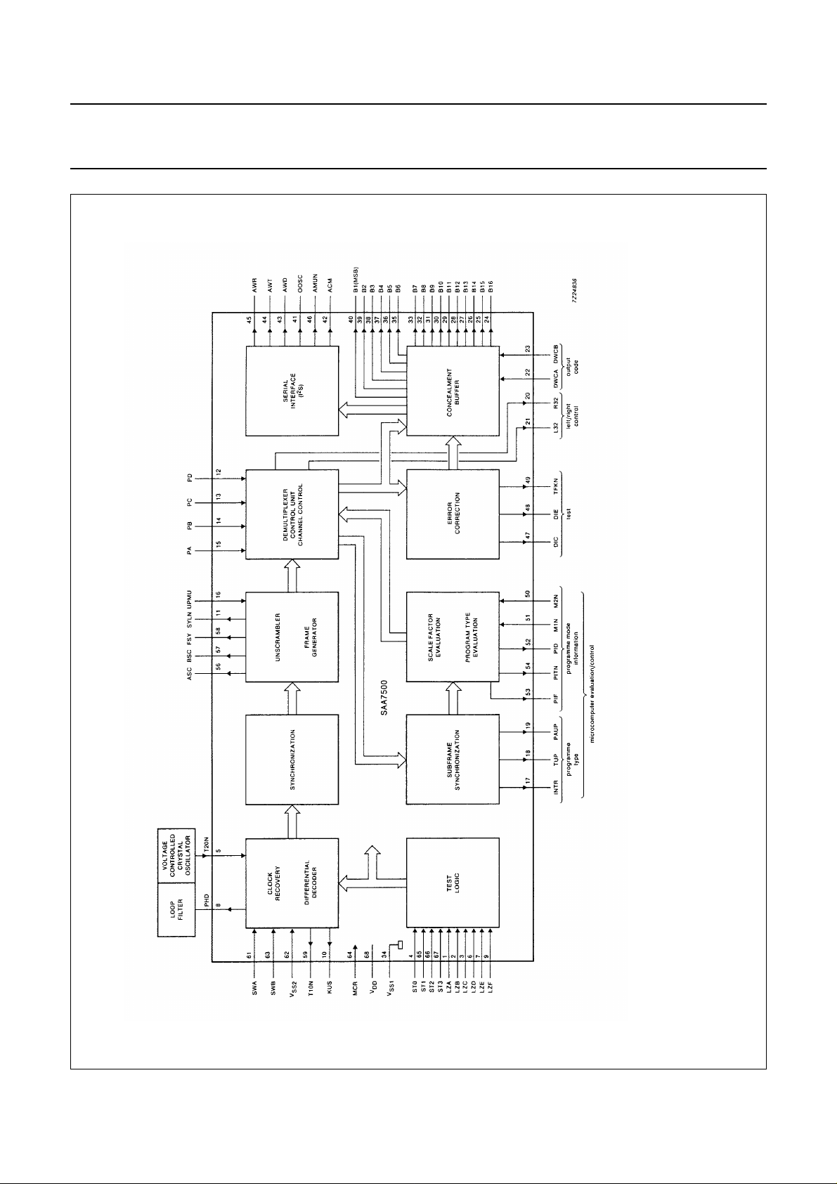
Fig.1 Block diagram.

Philips Semiconductors Product specification
Digital satellite radio broadcasting tuner
decoder (SAT-2)
PINNING
SAA7500
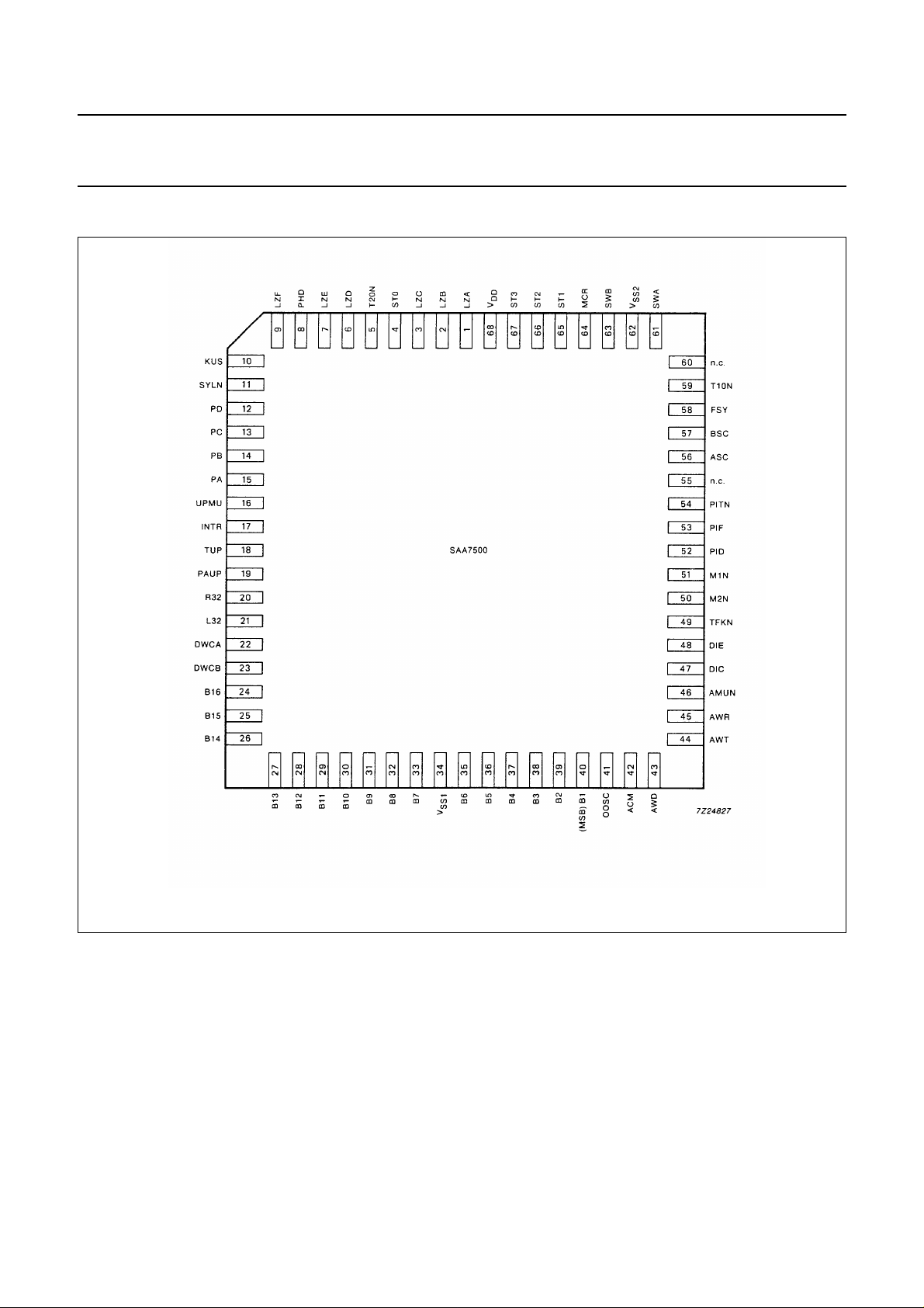
Fig.2 Pinning diagram; for pin functions see next page.
September 1989 4

Philips Semiconductors Product specification
Digital satellite radio broadcasting tuner
decoder (SAT-2)
Pin functions
(1) = CMOS level input. (2) = TTL level input. (3) = CMOS level input with pull down resistor.
PIN NO. MNEMONIC DESCRIPTION
1 LZA I(3) phase adjustment for the internal clock.
2 LZB I(3) phase adjustment for the internal clock.
3 LZC I(3) phase adjustment for the internal clock.
4 STO I(3) control input for testing.
5 T20N I(1) 20.48 MHz clock input from voltage controlled oscillator (VCX).
6 LZD I(3) control input for testing.
7 LZE I(3) control input for testing.
8 PHD O phase control signal for VCX.
9 LZF I(3) control input for testing.
10 KUS O test output (A’B’ swap).
11 SYLN O synchronization indication flag.
12 PD I(2) programme number input selector (MSB).
13 PC I(2) programme number input selector.
14 PB I(2) programme number input selector.
15 PA I(2) programme number input selector (LSB).
16 UPMU I(2) mute input (controlled by microcomputer).
17 INTR O interrupt flag for microcomputer.
18 TUP O programme type interface (clock).
19 PAUP O programme type interface (data).
20 R32 O multiplex control signal for right channel.
21 L32 O multiplex control signal for left channel.
22 DWCA I(3) DA-converter mode select input.
23 DWCB I(3) DA-converter mode select input.
24-33 B16-7 O audio data for parallel interface, bits 16 (LSB) to 7.
34 V
35-40 B6-1 O audio data for parallel interface, bits 6 to 1 (MSB).
41 OOSC O 4.096 MHz clock output.
42 ACM O concealment flag (for SAA7220P/C).
43 AWD O audio data (for SAA7220P/C).
44 AWT O bit clock (for SAA7220P/C).
45 AWR O word select signal (for SAA7220P/C).
46 AMUN O mute signal (for SAA7220P/C).
47 DIC O data output for testing.
48 DIE O data output for testing.
SS1
I ground (supply).
SAA7500
September 1989 5

Philips Semiconductors Product specification
Digital satellite radio broadcasting tuner
SAA7500
decoder (SAT-2)
PIN NO. MNEMONIC DESCRIPTION
49 TFKN O burst clock for test data.
50 M2N I(2) channel mode select input.
51 M1N I(2) channel mode select input.
52 PID O programme information (PI) interface output (data).
53 PIF O programme information (PI) interface output (window signal).
54 PITN O programme information (PI) interface output (clock).
55 n.c. not connected.
56 ASC O data output for 10.24 Mbit/s interface.
57 BSC O data output for 10.24 Mbit/s interface.
58 FSY O window signal for 10.24 Mbit/s interface.
59 T10N O 10.24 MHz clock output.
60 n.c. not connected.
61 SWA I(2) 10.24 Mbit/s data input.
62 V
63 SWB I(2) 10.24 Mbit/s data input.
64 MCR I(1) master reset.
65 ST1 I(3) control input for testing.
66 ST2 I(3) control input for testing.
67 ST3 I(3) control input for testing and mode select for 10.24 Mbit/s interface.
68 V
SS2
DD
I ground (screen).
I power supply.
September 1989 6
 Loading...