

Philips SAA7392HL-M2, SAA7392HL-M3, SAA7392HL-M3A Datasheet

DATA SH EET
Preliminary specification
File under Integrated Circuits, IC01
2000 Mar 21
INTEGRATED CIRCUITS
SAA7392
Channel encoder/decoder CDR60

2000 Mar 21 2
Philips Semiconductors Preliminary specification
Channel encoder/decoder CDR60 SAA7392
CONTENTS
1 FEATURES
2 GENERAL DESCRIPTION
3 QUICK REFERENCE DATA
4 ORDERING INFORMATION
5 BLOCK DIAGRAM
6 PINNING INFORMATION
6.1 Pinning
6.2 Pin description
7 FUNCTIONAL DESCRIPTION
7.1 Microprocessor interfaces
7.2 Register map
7.3 System clocks
7.4 HF analog front-end
7.5 Bit recovery
7.6 Decoder function
7.7 Subcode interface
7.8 Digital output
7.9 Serial output interface
7.10 Motor control
7.11 The serial in function
7.12 The subcode insert function
7.13 The data encoder block
7.14 Encode control block
7.15 The EFM modulator
7.16 The EFM clock generator
7.17 The Wobble processor
8 LIMITING VALUES
9 OPERATING CHARACTERISTICS
9.1 ADC and AGC parameters
10 APPLICATION INFORMATION
10.1 Write startcontrol of encoder in CD-ROM mode
10.2 Write start control of encoder in Audio mode
10.3 Start-up of encode in flow-control operation
10.4 Start-up of encoder in synchronous stream
mode
10.5 Operating CDR60 in CAV mode, flow control
on input stream
10.6 Operating in CLV Mode, Flow Control on Input
Stream
10.7 Operating in CLV Mode, Synchronous Stream
Operation
11 PACKAGE OUTLINE
12 SOLDERING
12.1 Introduction to soldering surface mount
packages
12.2 Reflow soldering
12.3 Wave soldering
12.4 Manual soldering
12.5 Suitability of surface mount IC packages for
wave and reflow soldering methods
13 DEFINITIONS
14 LIFE SUPPORT APPLICATIONS
15 PURCHASE OF PHILIPS I2C COMPONENTS
2000 Mar 21 3
Philips Semiconductors Preliminary specification
Channel encoder/decoder CDR60 SAA7392
1 FEATURES
• Very high speed Compact Disc (CD) compatible
decoding and encoding device
• On-chip Analog-to-Digital Converter (ADC) and
Automatic Gain Control (AGC) for HF data capture
• Eight-to-Fourteen Modulation (EFM)
• Advanced motor control loop to allow CAV, CLV and
pseudo-CLV playback
• Integrated FIFO for de-coupling of mechanism speed
and application speed
• Versatile output interface allowing different I2S-bus and
Electronic Industries Association of Japan (EIAJ)
formats
• Device is fully compatible with ELM, PLUM and Sanyo
CD-ROM block decoders
• Quad-pass CIRC correction for CD mode
(C1-C2-C1-C2)
• Subcode/header processing for CD format
• Frequency multiplier allows use of a 8 MHz crystal.
2 GENERAL DESCRIPTION
CDR60 is a channel encoder/decoder for
CD/CD-R/CD-RW/CD Audio Recorder systems. It
incorporates all logic and RAM required for the complete
encoding and decoding processes.
There aretwo main datapathsthrough the CDR60 device.
The decode datapath captures the incoming EFM data
stream via the HF ADC and AGC functions.
The bit detector recovers the individual bits from the
incoming signal, correcting asymmetry, performing noise
filtering and equalisation, and recovering the channel bit
clock using a digital PLL. The demodulator converts the
EFM bits to byte-wide data symbols, before passing them
onto the decoder for subcode extraction, de-interleaving
and error correction. The decoded data is then made
available via the multi-function serial output interface.
The encode datapath takes data symbols from the block
encoder/decoder via the serial data and subcode input
functions, encoding them via the encoder block. The
encoded data stream is passed to the EFM modulator,
which generates the required EFM signal, output as a
digital bitstream. Theencode process iscontrolled viathe
Wobble processor, encode control and EFM clock
generator functions.
As well as these two data processing sections, three
further blocks support overall device operation. The
system clockgenerator provides all digitalclocks required
by the CDR60. The motor servo allows the CDR60 to
control the spindle motor and is controlled by the
microprocessor interface. This interface can be accessed
either via a parallel (80C51) or a serial (I2C-bus) interface.
3 QUICK REFERENCE DATA
4 ORDERING INFORMATION
SYMBOL PARAMETER MIN. TYP. MAX. UNIT
V
DDD
supply voltage (core and pad ring) 3.0 3.3 3.6 V
V
DDA
supply voltage (analog) 3.0 3.3 3.6 V
V
DDE
supply voltage (output drivers) 3.0 3.3 3.6 V
I
DD
supply current − 200 − mA
f
xtal
crystal frequency 8 8.4672 33 MHz
T
amb
operating ambient temperature 0 − 70 °C
T
stg
storage temperature −55 − +125 °C
TYPE
NUMBER
PACKAGE
NAME DESCRIPTION VERSION
SAA7392HL LQFP80 plastic low profile quad flat package; 80 leads; body 12 × 12 × 1.4 mm SOT315-1
2000 Mar 21 4
Philips Semiconductors Preliminary specification
Channel encoder/decoder CDR60 SAA7392
This text is here in white to force landscape pages to be rotated correctly when browsing through the pdf in the Acrobat reader.This text is here in
_white to forcelandscape pages to be rotated correctly when browsing through the pdf in the Acrobat reader.This text is here inThistext is here in
white to force landscape pagesto be rotated correctly when browsingthrough the pdf in theAcrobatreader. white to force landscapepagesto be ...
5 BLOCK DIAGRAM
d
book, full pagewidth
SAA7392
MGR791
SUB-CPU INTERFACE
SERIAL OUT
51
PCAin
58
FLAG
54
STOPCK
59
DATAO
56
EBUOUT
55
V4
57
SYNC
61
BCLK
SERIAL IN
SUBCODE
INSERT
60
WCLK
64
DATAI
66
RCK
67
SFSY
65
SUB
34
INT
33
SDA
32
SCL
50
CSi
45
WRi
46
RDi
47
ALE
68
CFLG
35
to
42
DA7
to
DA0
ENCODE
CONTROL
27
PANIC
77
LASERON
EFM
MODULATOR
79
EFMDATA
IREF
GENERATOR
EFM CLOCK
GENERATOR
78
XEFM
WOBBLE
PROCESSOR
MOTOR/TACHO
INTERFACE
ERROR CORRECTOR
AND
MEMORY PROCESSOR
25
W441
26
ATIPSYC
6
WIN
2
WREFHI
3
WREFMID
1
8
WREFLO
RESET
28
PORE
TEST
CONTROL
17
TEST1
18
TEST2
SYSTEM CLOCK
GENERATOR
BIT DETECTOR DE-MODULATOR
21
XTLI
22
XTLO
24
MUXSWI
80
MEAS1
29
CL1
HF DATA
CAPTURE
12
AGCREF
13
HIN
10
HREFHI
14
HREFMID
11
HREFLO
IREF
7
VREF
23
OTD
4
5
15
16
30, 49, 53, 76
19, 31, 43, 48,
52, 62, 71, 75
20, 44, 63, 72
70
T1
69
T2
73
MOTO2/T3
74
MOTO1
V
SSA1
V
DDA1
V
DDA2
V
SSA2
V
SSD
V
DDD
V
DDE
Fig.1 Block diagram.
2000 Mar 21 5
Philips Semiconductors Preliminary specification
Channel encoder/decoder CDR60 SAA7392
6 PINNING INFORMATION
6.1 Pinning
Fig.2 Pin configuration.
handbook, full pagewidth
SAA7392
MGR792
1
2
3
4
5
6
7
8
9
10
11
12
13
14
15
16
17
18
19
WREFLO
WREFHI
WREFMID
V
SSA1
V
DDA1
WIN
VREF
IREF
n.c.
HREFHI
HREFLO
AGCREF
HIN
HREFMID
V
DDA2
V
SSA2
TEST1
TEST2
V
SSD
V
DDE
20
60
59
58
57
56
55
54
53
52
51
50
49
48
47
46
45
44
43
42
41
21
22
23
24
25
26
27
28
29
30
31
32
33
34
35
36
37
38
39
40
80
79
78
77
76
75
74
73
72
71
70
69
68
67
66
65
64
63
62
61
MEAS1
EFMDATA
XEFM
LASERON
V
DDDVSSD
MOTO1
MOTO2/T3
V
DDEVSSD
T1
T2
CFLG
SFSY
RCK
SUB
DATAI
V
DDEVSSD
BCLK
XTLI
XTLO
OTD
MUXSWI
W441
ATIPSYC
PANIC
PORE
CL1
V
DDD
V
SSD
SCL
SDA
INT
DA7
DA6
DA5
DA4
DA3
DA2
WCLK
DATAO
FLAG
SYNC
EBUOUT
V4
STOPCK
V
DDD
V
SSD
PCAin
CSi
V
DDD
V
SSD
ALE
RDi
WRi
V
DDE
V
SSD
DA0
DA1

2000 Mar 21 6
Philips Semiconductors Preliminary specification
Channel encoder/decoder CDR60 SAA7392
6.2 Pin description
Table 1 LQFP80 package; note 1
SYMBOL PIN TYPE DESCRIPTION
WREFLO 1 O wobble ADC analog reference voltage
WREFHI 2 O wobble ADC analog reference voltage
WREFMID 3 O wobble ADC analog reference voltage
V
SSA1
4 supply analog ground
V
DDA1
5 supply 3 V analog supply voltage 1; note 2
WIN 6 I wobble analog input
VREF 7 O analog voltage reference
IREF 8 O analog current reference
n.c. 9 − not connected
HREFHI 10 O HFADC analog reference voltage
HREFLO 11 O HF ADC analog reference voltage
AGCREF 12 I AGC analog reference voltage
HIN 13 I HF analog data input
HREFMID 14 O HFADC analog reference voltage
V
DDA2
15 supply 3 V analog supply voltage 2; note 2
V
SSA2
16 supply analog ground
TEST1 17 I test input 1
TEST2 18 I test input 2
V
SSD
19, 43, 62, 71 supply output driver ground
V
DDE
20 supply output driver 3 V supply voltage
XTLI 21 I crystal oscillator input
XTLO 22 O crystal oscillator output
OTD 23 I off track detect input
MUXSWI 24 I clock multiplier enable
W441 25 O wobble 44.1 kHz clock output
ATIPSYC 26 O ATIPSync output
PANIC 27 I laser low power (LLP)
PORE 28 I power-on reset
CL1 29 O divided clock output
V
DDD
30, 49, 53, 76 supply core and pad ring 3 V supply voltage; note 2
V
SSD
31, 48, 52, 75 supply core and pad ring ground
SCL 32 I sub-CPU clock
SDA 33 I/O bidirectional sub-CPU data
INT 34 O sub-CPU interrupt
DA7 35 I/O bidirectional sub-CPU parallel data bus
DA6 36 I/O bidirectional sub-CPU parallel data bus
DA5 37 I/O bidirectional sub-CPU parallel data bus
DA4 38 I/O bidirectional sub-CPU parallel data bus
2000 Mar 21 7
Philips Semiconductors Preliminary specification
Channel encoder/decoder CDR60 SAA7392
Notes
1. No signal may be applied to this device when it is not powered.
2. The analog and digital supply pins (V
DDA
and V
DDD
) must be connected to the same external supply.
DA3 39 I/O bidirectional sub-CPU parallel data bus
DA2 40 I/O bidirectional sub-CPU parallel data bus
DA1 41 I/O bidirectional sub-CPU parallel data bus
DA0 42 I/O bidirectional sub-CPU parallel data bus
V
DDE
44 supply output driver 3 V supply voltage
WRi 45 I sub-CPU write enable; active LOW
RDi 46 I sub-CPU read enable; active LOW
ALE 47 I sub-CPU address latch enable
CSi 50 I sub-CPU chip select
PCAin 51 I PCA input
STOPCK 54 O stop clock output
V4 55 O serial subcode output
EBUOUT 56 O digital output
SYNC 57 O I
2
S sector sync output
FLAG 58 O I
2
S correction flag
DATAO 59 O I
2
S data output
WCLK 60 I/O bidirectional I
2
S word clock
BCLK 61 I/O bidirectional I
2
S bit clock
V
DDE
63 supply output driver 3 V supply voltage
DATAI 64 I I
2
S data input
SUB 65 I EIAJ subcode data
RCK 66 O EIAJ subcode clock
SFSY 67 I EIAJ subcode sync
CFLG 68 O correction statistics; open-drain
T2 69 I tacho control input 2
T1 70 I tacho control input 1
V
DDE
72 supply output driver 3 V supply voltage
MOTO2/T3 73 I/O motor output 2/tacho input 3
MOTO1 74 O motor control output 1
LASERON 77 O laser write control
XEFM 78 O EFM clock output
EFMDATA 79 O EFM data output
MEAS1 80 O front end telemetry; open-drain
SYMBOL PIN TYPE DESCRIPTION
2000 Mar 21 8
Philips Semiconductors Preliminary specification
Channel encoder/decoder CDR60 SAA7392
7 FUNCTIONAL DESCRIPTION
7.1 Microprocessor interfaces
The SAA7392 is programmed via two independent
microprocessor interfaces:
• Serial I2C-bus
– SDA=I2C-bus data
– SCL = I2C-bus clock
–I2C-bus write address = 3EH
–I2C-bus read address = 3FH.
• Parallel 80C51 compatible
– DA(7:0) = address/data bus
– ALE = address latch enable; latches the address
information on the bus
– WRi = active LOW write signal; write to SAA7392
– RDi = active LOW read signal; read from SAA7392
– CSi = chip select signal; gates the RDi and WRi
signals.
7.1.1 S
ERIAL I
2
C-BUS INTERFACE
Data is transferred over the interface in single bytes, via
write data or read data commands.
The sequence for a write data command is as follows:
1. Send START condition
2. Send address 3EH (write)
3. Write register address byte
4. Write data byte
5. Send STOP condition.
The sequence for a read data command is as follows:
1. Send START condition
2. Send address 3EH (write)
3. Write status register address byte
4. Send STOP condition
5. Send address 3FH (read)
6. Read data byte
7. Send STOP condition.
7.1.2 P
ARALLEL INTERFACE
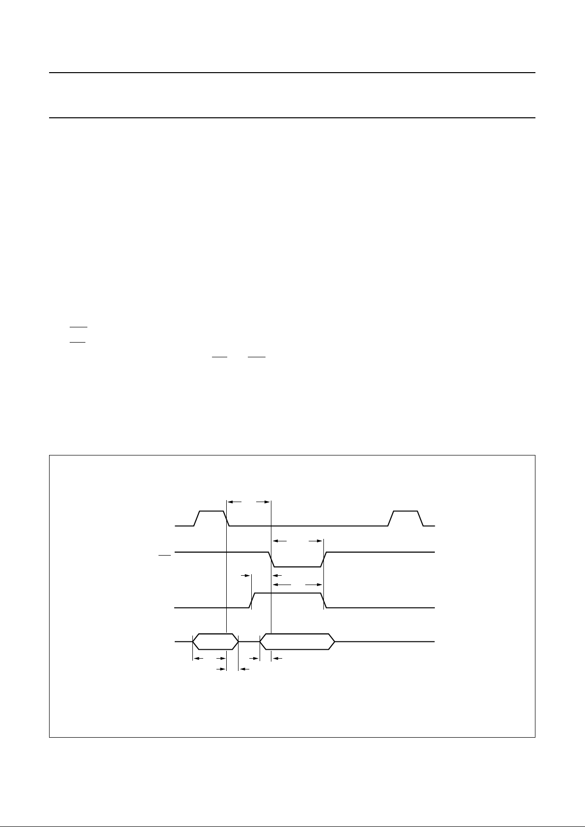
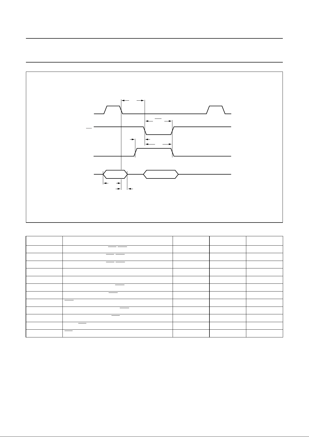
The parallelinterface hasa multiplexed address/databus.
Information can be written to or read from the SAA7392
using the protocols shown inFigs 3 and 4; specific timings
are shownin Table 2. Notethat only thelower six address
bits are decoded; so writing to address 40H would have
the same effect as writing to address 00H.
handbook, full pagewidth
MGR793
ALE
WRi
CSi
DA0 to DA7
address (0:7)
IN
data (0:7)
IN
t
d1
t
WRiL
t
h1
t
d2
t
su2
t
su1
t
h2
Fig.3 Microprocessor write protocol.
2000 Mar 21 9
Philips Semiconductors Preliminary specification
Channel encoder/decoder CDR60 SAA7392
handbook, full pagewidth
MGR794
ALE
RDi
CSi
DA0 to DA7
address (0:7)
IN
data (0:7)
OUT
t
d1
RDi
L
t
h1
t
d2
t
su1
t
h2
Fig.4 Microprocessor read protocol.
Table 2 Parallel interface timing
Note
1. T
clk
is the system clock period.
SYMBOL DESCRIPTION MIN.
(1)
MAX.
(1)
UNIT
t
d1
Delay ALE falling to RDi/WRi falling. 17 − ns
t
d2
Delay CSi rising to RDi/WRi falling. 17 − ns
t
h1
CSi hold time after RDi/WRi falling. 2T
clk
+17 − ns
t
su1
Address setup time before ALE falling. 17 − ns
t
h2
Address hold time after ALE falling. 17 − ns
t
su2
Data setup time before WRi falling. 0 − ns
t
h3
Data hold time after WRi falling. 2T
clk
+17 − ns
t
WRiL
WRi LOW time. 1T
clk
+17 − ns
t
h4
ALE LOW hold time after WRi LOW. 3T
clk
+17 − ns
t
d3
Delay data valid after RDi LOW. − 3T
clk
+17 ns
t
d4
Delay RDi HIGH to data out high-impedance. − 17 ns
t
RDiL
RDi LOW time. 3T
clk
+ 128 − ns

2000 Mar 21 10
Philips Semiconductors Preliminary specification
Channel encoder/decoder CDR60 SAA7392
This text is here in white to force landscape pages to be rotated correctly when browsing through the pdf in the Acrobat reader.This text is here in
_white to forcelandscape pages to be rotated correctly when browsing through the pdf in the Acrobatreader.This text is here inThis text is here in
white to force landscape pagesto berotated correctlywhen browsing throughthe pdfin theAcrobat reader. whiteto forcelandscape pagesto be ...
7.2 Register map
Table 3 Register map
ADDRESS
(HEX)
REGISTER NAME TYPE FUNCTION
BLOCK
RESPONSIBLE
00 PLL Lock Select Register (PLLLock) Write PLL lock select bit detector
Read 8-bit PLL frequency bit detector
01 PLL Bandwidth Select Register (PLLSet) Write PLL bandwidth select bit detector
Read 8-bit asymmetry signal bit detector
02 PLL Frequency Preset Register (PLLFreq) Write PLL frequency preset bit detector
Read 8-bit jitter signal bit detector
03 PLL Equalizer Preset Register (PLLEqu) Write PLL equalizer preset bit detector
Read Observe internal lock flags bit detector
04 PLL Lock Aid2 Preset Register (PLLFMeas) Write PLL lock aid 2 preset bit detector
05 I2S Output Register 1 (Output1) Write I2S output 1 serial out
06 I
2
S Output Register 2 (Output2) Write I2S output 2 serial out
07 I
2
S Output Register 3 (Output3) Write I2S output 3 serial out
08 Semaphore Register 1 (Sema1) Write/Read Inter-microprocessor
communication
sub-CPU
09 Semaphore Register 2 (Sema2) Write/Read Inter-microprocessor
communication
sub-CPU
0A Semaphore Register 3 (Sema3) Write/Read Inter-microprocessor
communication
sub-CPU
0B Interrupt Enable Register (IntEn) Write Enable interrupts sub-CPU
0B Status Register (Status) Read Interrupt status sub-CPU
0C Motor Control Register1 (Motor1) Write Frequency set-point motor/tacho
Read 8-bit slicer compensation
value
bit detector
0D Motor Mode Select Register2 (Motor2) Write Motor coefficient preset motor/tacho
Read Opening of eye pattern bit detector
0E Motor Control Register 3 (Motor3) Write Motor integrator preset motor/tacho
Read Read back of motor frequency motor/tacho
0F Motor Control Register 4 (Motor4) Write Motor control motor/tacho
10 Motor Control Register 5 (Motor5) Read/Write Motor integrator value motor/tacho
11 Motor Control Register 6 (Motor6) Read/Write Motor integrator value motor/tacho

2000 Mar 21 11
Philips Semiconductors Preliminary specification
Channel encoder/decoder CDR60 SAA7392
This text is here in white to force landscape pages to be rotated correctly when browsing through the pdf in the Acrobat reader.This text is here in
_white to forcelandscape pages to be rotated correctly when browsing through the pdf in the Acrobatreader.This text is here inThis text is here in
white to force landscape pagesto berotated correctlywhen browsing throughthe pdfin theAcrobat reader. whiteto forcelandscape pagesto be ...
12 Clock Preset Register (ClockPre) Write Clock control clock generator
Read Status of Q-channel subcode encoder/decoder
13 Decoder Mode Select Register (DecoMode) Write Decoder mode select encoder/decoder
Read Q-channel subcode data encoder/decoder
14 Subcode Read End Register (SubReadEnd) Read Subcode data read finished encoder/decoder
15 Analog Settings Register 1 (AnaSet1) Write Analog control analog
Read C1 frames in FIFO + offset encoder/decoder
16 Viterbi Detector Settings Register (VitSet) Write Viterbi detector control bit detector
17 Tacho Gain Setting Register (Tacho1) Write Tacho gain setting motor/tacho
18 Tacho Trip Setting Register (Tacho2) Write Tacho trip setting motor/tacho
19 Tacho Control Register (Tacho3) Write Tacho control settings motor/tacho
1B Soft Reset Register (SoftReset) Write Sub-block reset sub-CPU
1D Motor Control Register7 (Motor7) Write Control coefficients select motor/tacho
1E Input Configuration Register (InputConfig) Write EBU clock frequency and
input format
serial input
20 Status Register 2 (Status2) Read/Write Interrupt status sub-CPU
21 Interrupt Enable Register 2 (IntEn2) Write Enable interrupts sub-CPU
22 Subcode Preset Count Register (SubPresetCount) Write Preset count field subcode insert
Read Current count field subcode insert
23 Subcode Configuration Register 1 (SubConfig1) Write Subcode control subcode insert
24 Subcode Configuration Register 2 (SubConfig2) Read/Write Subcode control subcode insert
25 Subcode Start Data Register (SubStartData) Write Subcode control subcode insert
26 Subcode Data Register (SubData) Read/Write Subcode data subcode insert
27 Wobble Configuration Register1 (WobbleConfig1) Integrator and loop bandwidth Wobble processor
Window width ATIP syncs Wobble processor
28 Wobble Configuration Register2 (WobbleConfig2) Write Wobble PLL control Wobble processor
29 ATIP Status Register (ATIPStatus) Read ATIP status Wobble processor
2A Wobble Frequency Register 1 (WobbleFreq1) Read/Write 8 MSBs of PLL frequency Wobble processor
2B Wobble Frequency Register 2 (WobbleFreq2) Read/Write 8 LSBs of PLL frequency Wobble processor
2C ATIP Data Register (ATIPData) Read ATIP data Wobble processor
ADDRESS
(HEX)
REGISTER NAME TYPE FUNCTION
BLOCK
RESPONSIBLE

2000 Mar 21 12
Philips Semiconductors Preliminary specification
Channel encoder/decoder CDR60 SAA7392
This text is here in white to force landscape pages to be rotated correctly when browsing through the pdf in the Acrobat reader.This text is here in
_white to forcelandscape pages to be rotated correctly when browsing through the pdf in the Acrobatreader.This text is here inThis text is here in
white to force landscape pagesto berotated correctlywhen browsing throughthe pdfin theAcrobat reader. whiteto forcelandscape pagesto be ...
2D ATIP Data End Register (ATIPDataEnd) Read Least significant byte ATIP
data
Wobble processor
2E Wobble Peak Status Register (WobbleStatus) Read Peak value of wobble signal Wobble processor
30 Encode WriteOn Control Register (EncodeWContr) Read/Write Laser and data flow control encode control
31 Encode Start Offset Register (EncodeStartOffset) Write Start WriteOn flags delay encode control
32 Encode Stop Offset Register (EncodeStopOffset) Write Stop WriteOn flags delay encode control
33 Encode Offset Register (EncodeXOffset) Write 10-bit value for Xoffset encode control
34 EFM Clock Configuration Register 1 (EFMClockConf1) Write EFM clock control EFM clock generator
35 EFM Clock Configuration Register 2 (EFMClockConf2) Write EFM clock control EFM clock generator
36 EFM Clock Configuration Register 3 (EFMClockConf3) Write EFM clock control EFM clock generator
Read Integrator value EFM clock generator
37 EFM PLL Frequency Register (EFMPLLFreq) Read EFM PLL frequency EFM clock generator
37 EFM Clock Configuration Register 4 (EFMClockConf4) Write EFM clock control EFM clock generator
38 ATIP Error Register (ATER) Read Counter for ATIP CRC errors sub-CPU
39 C1 Block Error Register (C1BLER) Read Counter for C1 errors sub-CPU
3A C2 Block Error Register (C2BLER) Read Counter for C2 errors sub-CPU
3C EFM Preset Count Register (EFMPresetCount) Write EFM frame position for output EFM modulator
3D EFM Modulator Configuration Register (EFMModConfig) Write XEFM control and output data
format
EFM modulator
3E EFM Modulator Configuration Register 2 (EFMModConfig2) Write XEFM control and output data
format
EFM modulator
ADDRESS
(HEX)
REGISTER NAME TYPE FUNCTION
BLOCK
RESPONSIBLE

2000 Mar 21 13
Philips Semiconductors Preliminary specification
Channel encoder/decoder CDR60 SAA7392
7.2.1 INTERRUPT PIN
The interrupt pin (INT) is the AND-OR-INVERT of the Status and Interrupt Enable Registers, i.e. INT will become active
when corresponding bits are set at the same time in the Status and Interrupt Enable Registers.
7.2.2 THE SEMAPHORE REGISTERS (SEMA1, SEMA2 AND SEMA3)
The Semaphore Registers are intended for inter-microprocessor communications. For example, microcontroller 1 can
writedata tomicrocontroller 2 viaSema1 andmicrocontroller 2 can writedata tomicrocontroller 1 viaSema2. TheStatus
Register ofthe SAA7392offers a mechanismso that both microcontrollers cansee when newdata hasbeen written and
whenit hasbeen readby lookingat thecontents ofthe Semaphore Registers. Version M3of theCDR60 canbe identified
by writingand reading register Sema3. In version M3,bit 1 of Sema3is always read as logic 0, whereas inother CDR60
versions this bit reads the same value as what was written to it before.
7.2.2.1 Semaphore Register 1 (Sema1)
Table 4 Semaphore Register 1 (address 08H) - READ/WRITE
7.2.2.2 Semaphore Register 2 (Sema2)
Table 5 Semaphore Register 2 (address 09H) - READ/WRITE
7.2.2.3 Semaphore Register 3 (Sema3)
Table 6 Semaphore Register 3 (address 0AH) - READ/WRITE
7.2.3 S
TATUS REGISTER (STATUS)
Table 7 Status Register (address 0BH) - READ
Table 8 Description of Status bits
76543210
Sema1.7 Sema1.6 Sema1.5 Sema1.4 Sema1.3 Sema1.2 Sema1.1 Sema1.0
76543210
Sema2.7 Sema2.6 Sema2.5 Sema2.4 Sema2.3 Sema2.2 Sema2.1 Sema2.0
76543210
Sema3.7 Sema3.6 Sema3.5 Sema3.4 Sema3.3 Sema3.2 Sema3.1 Sema3.0
76543 210
Sema1 Sema2 Sema3 LockIn HeaderVal MotorOverflow FIFOOv −
BIT SYMBOL DESCRIPTION
7 Sema1 If Sema1 = 1, change in register Sema1 has been detected. Reset if register Sema1 read.
6 Sema2 If Sema2 = 1, change in register Sema2 has been detected. Reset if register Sema2 read.
5 Sema3 If Sema3 = 1, change in register Sema3 has been detected. Reset if register Sema3 read.
4 LockIn If LockIn = 1, then channel data PLL in lock (not latched).
3 HeaderVal HeaderVal is set when new header/subcode is available; reset on reading SubReadEnd.
2 MotorOverflow If MotorOverflow = 1, then a motor overflow is occurring (not latched).
1 FIFOOv If FIFOOv = 1, then the FIFO has overflowed.
0 − This bit is reserved.
2000 Mar 21 14
Philips Semiconductors Preliminary specification
Channel encoder/decoder CDR60 SAA7392
7.2.4 INTERRUPT ENABLE REGISTER (INTEN)
Table 9 Interrupt Enable Register (address 0BH) - WRITE
Table 10 Description of IntEn bits
7.2.5 S
TATUS REGISTER 2(STATUS2)
Table 11 Status Register 2 (address 20H) - READ/WRITE
Table 12 Description of Status2 bits
76543 2 10
Sema1En Sema2En Sema3En LockInEn HeaderValen MotorOverflowEn FIFOOvEn −
BIT SYMBOL DESCRIPTION
7 Sema1En If Sema1En = 1, then Semaphore Register 1 interrupt is enabled.
6 Sema2En If Sema2En = 1, then Semaphore Register 2 interrupt is enabled.
5 Sema3En If Sema3En = 1, then Semaphore Register 3 interrupt is enabled.
4 LockInEn If LockinEn = 1, then channel data PLL in lock interrupt is enabled.
3 HeaderValEn If HeaderValEn = 1, then new header/subcode available interrupt is enabled.
2 MotorOverflowEn If MotorOverflowEn = 1, then motor overflow interrupt is enabled.
1 FIFOOvEn If FIFOOvEn = 1, then FIFO overflow interrupt is enabled.
0 − This bit is reserved.
76 543210
BankSwitch SyncError DataNotValid QSync ATIPSync LaserOn LaserOff XErrorLarge
BIT SYMBOL DESCRIPTION
7 BankSwitch When set a ‘Bank switch’in the subcode insert blockhas occurred; reset when a logic 1
is written to this bit.
6 SyncError When set synchronisation with PLUM on subcode transfer has failed; reset when a
logic 1 is written to this bit.
5 DataNotValid When set an under-run on subcode transfer with PLUM has occurred; reset when a
logic 1 is written to this bit.
4 QSync When set a Q-channel subcode sync has been written to disc; reset when a logic 1 is
written to this bit.
3 ATIPSync When set sync has been found in the ATIP channel; reset when a logic 1 is written to
this bit.
2 LaserOn When set a rising edge of the internal LaserOn signal has occurred; reset when a
logic 1 is written to this bit.
1 LaserOff When set a falling edge of the internal LaserOn signal has occurred; reset when a
logic 1 is written to this bit.
0 XErrorLarge When set the offset between QSync and ATIPSync is more than 2 EFM frames different
from the programmed value.

2000 Mar 21 15
Philips Semiconductors Preliminary specification
Channel encoder/decoder CDR60 SAA7392
7.2.6 INTERRUPT ENABLE REGISTER 2(INTEN2)
Table 13 Interrupt Enable Register 2 (address 21H) - WRITE
Table 14 Description of IntEn2 bits
7.2.7 S
OFT RESET REGISTER (SOFTRESET)
Table 15 Soft Reset Register (address 1BH) - WRITE
Table 16 Description of SoftReset bits
76 543210
BankSwitchEnSyncErrorEn DataNotValidEnQSyncEn ATIPSyncEn LaserOnEn LaserOffEn XErrorLarge
En
BIT SYMBOL DESCRIPTION
7 BankSwitchEnIf BankSwitchEn = 1, then BankSwitch interrupt is enabled.
6 SyncErrorEn If SyncErrorEn = 1, then SyncError interrupt is enabled.
5 DataNotVali
dEn
If DataNotValidEn= 1, then DataNotValid interrupt is enabled.
4 QSyncEn If QSyncEn = 1, then QSync interrupt is enabled.
3 ATIPSyncEn If ATIPSyncEn = 1, then ATIPSync interrupt is enabled.
2 LaserOnEn If LaserOnEn = 1, then LaserOn interrupt is enabled.
1 LaserOffEn If LaserOffEn = 1, then LaserOff interrupt is enabled.
0 XErrorLargeEnIf XerrorLarge = 1, then XErrorLarge interrupt is enabled.
76543210
−−−−−−−SReset1
BIT SYMBOL DESCRIPTION
7to1 − These 7 bits are reserved.
0 SReset1 When set, synchronisation with PLUM on subcode transfer has failed; reset when
a logic 1 is written to this bit (Status2).
This bit is an active HIGH reset to the following blocks: Encoder/decoder, EFM
modulator, Encode control block, Serial input/output block and Encode subcode insert
block. The clock control, EFM PLL, tacho, motor interface and wobble interface remain
running.
Soft reset will reset the following registers: EFMPresetCount, EFMModulateConfig,
EFMModulateConfig2, EncodeXOffset, EncodeWriteControl, EncodeStartOffset,
EncodeStopOffset, SubPresetCount, SubConfig1, Subconfig2,SubStartData, SubData,
InputConfig, DecoMode, Output1, Output2 and Output3.
A soft reset is mandatory in the following cases:
1. After programming the BCLK clock
2. When switching from encode to decode
3. When switching from decode to encode.
2000 Mar 21 16
Philips Semiconductors Preliminary specification
Channel encoder/decoder CDR60 SAA7392
7.3 System clocks
The principleclocks used inthe SAA7392 are derived from the crystaloscillator input pinXTLI (alternatively, anexternal
clock can be connected to this pin). These clocks are the system clock (also used as the ADC clock) and the I2S output
bit clock (BCLK).
The system clock (f
clk
) defines the maximumoperational channel rate for the device. The maximum EFM channel clock
is twice the system clock, for CD it is equivalent tosystem clock/(4.3 × 106) which is approximately 11.5 × CDROM for a
25 MHz system clock.
The other clock in the system is the channel data clock, this is recovered by the front-end bit recovery PLL.
Fig.5 System clock generator.
handbook, full pagewidth
MGR795
MUXSWI
XTLI
XTLO
CL1
system clock
SYSTEM
CLOCK
DIVIDER
BCLK
XTLI
M × XTLI
BIT
CLOCK
DIVIDER
system clock
CL1
DIVIDER
CLOCK
(1)
MULTIPLIER
×
crystal
oscillator
(1) M = 1 if MUXSWI is LOW; M = 8 if MUXSWI is HIGH.
2000 Mar 21 17
Philips Semiconductors Preliminary specification
Channel encoder/decoder CDR60 SAA7392
7.3.1 CLOCK PRESET REGISTER (CLOCKPRE)
Table 17 Clock Preset Register (address 12H) - WRITE
Table 18 Description of ClockPre bits
Table 19 Selection of system clock frequency
Table 20 Selection of BCLK frequency
76543210
CL1Div GateBClk Div.1 Div.0 Mux2 Div2.2 Div2.1 Div2.0
BIT SYMBOL DESCRIPTION
7 CL1Div If CL1Div = 0, then CL1 output frequency is
1
⁄3f
clk
. If CL1Div = 1, then CL1 output
frequency is1⁄2f
clk
.
6 GateBClk If GateBClk = 0, then I
2
S output bit clock gating is disabled. If GateBClk = 1, then I2S
output bit clock gating enabled, BCLK is output, clock is automatically stopped if FIFO
underflows (this is known as Flow control mode).
5 Div.1 These 2 bits select the system clock frequency (f
clk
); see Table 19. This frequency
should be programmed for the expected disc channel rate (e.g. 4.33 MHz for 1 × CD)
within the following constraints:
In this clock range, reliable bit detection is possible. All data found will be written to the
FIFO. It is the responsibility of the user to select system clock values so that the FIFO
performance is controlled.
4 Div.0
3 Mux2 If Mux2 = 0, then N (bit clock divider pre-scaler) = 1. If Mux2 = 1, then N = M.
2 to 0 Div2<2:0> These 3 bits select the BCLK frequency (f
BCLK
); see Table 20. It is the responsibility of
the user to select BCLK values so that the FIFO performance is controlled.
Div.1 Div.0 SYSTEM CLOCK FREQUENCY (f
clk
)
00M×f
XTLI
0 1 0.5 × M × f
XTLI
1 0 0.25 × M × f
XTLI
1 1 0.125 × M × f
XTLI
Div2.1 Div2.1 Div2.0 BCLK FREQUENCY (f
BCLK
)
000N×f
XTLI
001N×f
XTLI
010
1
/
2
(N × f
XTLI
)
011
1
/
3
(N × f
XTLI
)
100
1
/
4
(N × f
XTLI
)
101
1
/
6
(N × f
XTLI
)
110
1
/
8
(N × f
XTLI
)
111
1
/
12
(N × f
XTLI
)
Channel rate
2
----------------------------------
f
clk
4 Channel rate×<<

2000 Mar 21 18
Philips Semiconductors Preliminary specification
Channel encoder/decoder CDR60 SAA7392
7.4 HF analog front-end
The HF ADC in the SAA7392 encodes the EFM high
frequency signal from the disc light pen assembly. These
signals are pre-processed, externally to the SAA7392, by
either AEGER-2 or a DALAS equivalent. The dynamic
range of the ADC is optimized by the inclusion of an
AC coupled AGC function under digital control.
In order to make use of the whole digital front-end
resolution, the output of the gain control amplifier should
constantly deliver 1.4 V
(p-p)
output signal. The gain range
ofthe ADC isapproximately14 dB, with32 steps. Thegain
control for the variable gain amplifier is controlled by an
on-chip digital gaincontrol block (AGC). This blockallows
for both automatic and microprocessor gain control. The
gain control block will detect ADC extreme conditions
(00H or FFH outputs); on these values the gain control
block will decrement the gain. If no extreme codes occur
the gain is incremented.
7.4.1 FIXED GAIN
Control of the gain is as follows:
1. Writing XX1X XXXX to the Anaset1 register
(address 15H) increases the AGC gain by 1.1 dB
2. Writing XX0X XXXX to the AnaSet1 register
(address 15H) decreases the AGC gain by 1.1 dB
3. Instructions to increment/decrement gain are ignored
when the AGC gain limits of −4/+12 dB are reached.
7.4.2 AUTOMATIC GAIN CONTROL (AGC)
The gain of theAGC cellis adjusteduntil the analog signal
at the ADC input extends over the complete range of
the ADC.Detection ofthis conditionis in thedigital domain
where the maximum and minimum ADC codes are
measured. The dynamics of the AGC system are as
follows.
1. If the ADC output codes are not full scale (i.e.
000 0000 and 111 11111) the AGC gain is
incremented in 1.1 dB steps with a time constant of
1000/n µs, where n is the over-speed factor i.e. n = 1
for basic audio CD.
2. When full scale is detected at the output of the ADC
the AGC gain is fixed provided that full scale is
maintained and clipping does not occur for greater
than 20% of the time.
3. If clipping occurs for more than 20% of the time, then
the AGC gain is reduced in 1.1 dB steps with a time
constant of 60/n µs.
The ADC and AGC electrical characteristics are specified
in Chapter 9.
7.4.3 ANALOG SETTINGS REGISTER 1(ANASET1)
Table 21 Analog Settings Register 1 (address 15H) - WRITE
Table 22 Description of AnaSet1 bits
76543210
GainControl MaxGain StepUp StepDown PowerDown −−−
BIT SYMBOL DESCRIPTION
7 GainControl If GainControl = 0, then gain control is in Hold mode. If GainControl = 1, then automatic
gain control is on.
6 MaxGain If MaxGain = 0, then there is no gain limit. If MaxGain = 1, then the maximum gain is
7.66 dB.
5 StepUp If StepUp = 1, then step up gain by one LSB.
4 StepDown If StepDown = 1, then step down gain by one LSB.
3 PowerDown If PowerDown = 0, then analog blocks are powered up. If PowerDown = 1, then analog
blocks are powered down.
2to0 − These 3 bits are reserved and must be set to a logic 0s.
2000 Mar 21 19
Philips Semiconductors Preliminary specification
Channel encoder/decoder CDR60 SAA7392
7.5 Bit recovery
The bit recovery block (shown in Fig.6) contains the slice
levelcircuitry, anoise filtertolimit theHF-EFMsignal noise
contribution, an adaptive slicer circuit and a digital PLL.
These blocks can be controlled via the microprocessor.
The channel rate should always obey the following
constraints:
• It should be less than 2 × the system clock
• It should be greater than 0.25 × the system clock.
In this clock range reliable bit clock detection is possible.
All data found will be written to the FIFO. It is the
responsibility ofthe user toselect BCLK and system clock
values so that the FIFO operation is controlled.
The digital noise filter runs on the PLL bit clock and limits
the bandwidthof the incomingsignal to 0.25 ofthe PLL bit
clock frequency. The characteristics of the filter are:
• Passband: 0 to 0.22 f
b
• Stopband: 0.28 fb to (f
clk
− 0.28 fb)
• Rejection: −28 dB.
The slice level determination circuit compensates the
incoming signalasymmetry component. Thebandwidth of
this circuit is programmable via register PLLSet.
A programmable (one tap presetable, asymmetrical)
equaliser is used in the bit detection circuit. The first and
last tap settings are different. Possible tap values are
settable via register PLLEqu.
The advanced detector has two extra detection circuits
(adaptive slicer and run length 2 push-back) which are
controlled via the VitSet register, that allow improved
margin in the bit detector.
The adaptive slicer does a second stage slice operation;
thebandwidth ishigherthan thefirst slicer. Itcan beturned
on/off via the VitSet register.
If the advanced detector is switched on all run length 2
symbols are pushed back to run length 3. The circuit will
determine thetransition that was most likely to bein error,
and shift the transition on that edge.
Fig.6 Block diagram of bit recovery block.
handbook, full pagewidth
MGR796
+
−
GAIN CONTROLLED
AMPLIFIER
+
MEAS1
clocked on PLL clock
MULTIPLEXER
jitter value
PLL frequency
slice level
RMS JITTER
MEASUREMENT
VITERBI
DETECTOR
DIGITAL
EQUALIZER
NOISE
FILTER
ADC
ZERO TRANS
DETECTOR
SLICE LEVEL
DETERMINE
GAIN CONTROL
BLOCK
DIGITAL
PLL
HIN

2000 Mar 21 20
Philips Semiconductors Preliminary specification
Channel encoder/decoder CDR60 SAA7392
7.5.1 DIGITAL PLL
The digital PLL will recover the channel bit clock. As the
capturerange ofthe PLLitselfis limited,lockdetectors and
2 capture aids are present. In total three different PLL
operation modes exist: In-lock, Inner-lock aid and
Outer-lock aid.
The PLL behaviour during in-lock (the normal on-track
situation) can be best explained in the frequency domain.
The PLL operation is completely linear during in-lock
situations. The open-loop response of the PLL is given in
Fig.7. The three frequencies, f0(integrator cross-over
frequency), f1(PLL bandwidth) and f2(low-pass
bandwidth) are programmable via register PLLSet.
To extend the PLL capture range two lock aids are used:
• Inner lock aid: has a capture range of ±10% and will
bring the PLL frequency to the lock point
• Outer lock range: has no limitation on capture range,
and will bring the PLL within the range of the inner lock
range.
Two outer lock aids can be used:
• Run length 3 deviation detector: this circuit is known to
be sensitive to systematic over/under equalization; this
over/under equalizationcan becounter-acted by writing
a non-zero phase offset value to register PLLLock.
• Frequency measurement detector: this circuit regulates
the PLL frequency so that the average number of EFM
transitions is a fixed fraction of the PLL bit clock; the
transition frequency is settable via register PLLFMeas.
Programmability/observability is built into the PLL. Its
operation can be influenced in two ways:
• It is possible to select the state the PLL is in (in-lock,
near-lock, outer-lock) via register PLLLock
• It is possible to preset the PLL frequency to a certain
value via registers PLLEqu and PLLFreq.
The operation of the bit detector can be monitored by the
microprocessor and via the MEAS1 pin. Four signals are
available for measurement:
• PLL frequency signal: the most significant 8 bits are
available via register PLLLock
• Asymmetry signal: the 8-bit signal in 2’s complement
form is available via register PLLSet
• Jitter signal: the most significant 8 bits are available via
register PLLFreq. This gives an impression of the
detection jitter after all processing is done.
jitter<9:0> = average ((jitter individual
transition)2× 8192)
To obtain the jitter in the bit clocks the jitter<9:0> value
must be divided by 8192 and square routed. Note that
the jitter<9:0> overestimates thejitter (byapproximately
rms jitter increase of 0.03 bit clock), because the
quantization of the zero transitions is in 4 intervals.
Note the jitter is measured before the bit detection and
contains contributions due to various imperfections in
the complete signal path; i.e. disc, preamplifier, ADC,
limited bitwidths, PLL performance, internal filter noise,
asymmetry compensation, equalizer.
• Internal lock flags: The internally generated inner-lock
signal (f_lock_in), lock signal (lock_in) and flag that
indicates when a run length 14 is detected
(long_symbol) are available via register PLLEqu.
Fig.7 PLL bode diagram.
MGR797
handbook, halfpage
frequency (Hz)
amplitude
(dB)
f
0f1
f
2
2000 Mar 21 21
Philips Semiconductors Preliminary specification
Channel encoder/decoder CDR60 SAA7392
7.5.2 MEAS1 PIN
The MEAS1 pin carries the 3 measurement signals: jitter
(sampled twice), PLL frequency, and asymmetry. Each
frame consists of 64 bits (each 4 system clock periods
long), beginning with a start bit, then data bits then pause
bits (see Fig.8). The start bit is always preceded by
17 pause bits; and the intermediate start bits at
locations 12, 24 and 36 guarantee that no other ‘1’ bit is
preceded by 17 ‘0’ bits, making the start detection easy.
The structure of the frame is described in Table 23 and
shown in Fig.8.
Table 23 Frame structure
BIT VALUE FUNCTION
0 logic 1 start bit
1 to 10 jitter<9:0> jitter word
11 logic 0
12 logic 1 intermediate start bit
13 to 22 pllfreq<9:0> PLL frequency word
23 logic 0
24 logic 1 intermediate start bit
25 to 32 assym<7:0> asymmetry word
33 logic 0
34 logic 1 intermediate start bit
37 to 46 jitter<9:0> second sample of jitter
word
47 to 63 logic 0 pause
Fig.8 Format on MEAS1 pin.
MGR798
handbook, halfpage
bit 0 bit 1
start
bit
pause data bits
bit 2 bit 3
2000 Mar 21 22
Philips Semiconductors Preliminary specification
Channel encoder/decoder CDR60 SAA7392
7.5.3 PLL LOCK SELECT REGISTER (PLLLOCK)
The behaviour of this register is dependent upon whether its being read or written. The behaviour for the write operation
is described in Tables 24 to 27. When read the 8 MSBs of the PLL frequency counter are returned; this is described in
Tables 24 and 28.
Table 24 PLL Lock Select Register (address 00H) - WRITE/READ
Table 25 Description of PLLLock bits for write operation
Table 26 Selection of phase override setting
Table 27 Selection of PLL lock
76543210
LockOride PhaOset.2 PhaOset.1 PhaOset.0 PLLForceL.3 PLLForceL.2 PLLForceL.1 PLLForceL.0
PLLFreq.7 PLLFreq.6 PLLFreq.5 PLLFreq.4 PLLFreq.3 PLLFreq.2 PLLFreq.1 PLLFreq.0
BIT SYMBOL DESCRIPTION
7 LockOride When LockOride = 0, then automatic lock behaviourselected, PLLForceL<3:0>must be
set to ‘0000’. When LockOride = 1, then PLL manual override, PLLForceL<3:0> must
also be programmed.
6 PhaOset.2 These 3 bits are used to select the phase override settings; see Table 26.
5 PhaOset.1
4 PhaOset.0
3 PLLForceL.3 These 4 bits are used to select the PLL lock; see Table 27.
2 PLLForceL.2
1 PLLForceL.1
0 PLLForceL.0
PhaOset.2 PhaOset.1 PhaOset.0 PHASE OVERRIDE
0 0 0 reserved
001
3
/
8
×PLL clock over-equalized T3
010
2
/
8
×PLL clock over-equalized T3
011
1
/
8
×PLL clock over-equalized T3
1 0 0 correct equalisation
101
1
/
8
×PLL clock under-equalized T3
110
2
/
8
×PLL clock under-equalized T3
111
3
/
8
×PLL clock under-equalized T3
PLLForceL.3 PLLForceL.2 PLLForceL.1 PLLForceL.0 PLL LOCK
0000automatic lock behaviour
0001force PLL in-lock
0100force PLL into outer-lock
0110force PLL into inner-lock
1000force PLL into Hold mode (PLL frequency can be
forced using preset value in register PLLFreq)
XXXXall other combinations are reserved
2000 Mar 21 23
Philips Semiconductors Preliminary specification
Channel encoder/decoder CDR60 SAA7392
Table 28 Description of PLLock bits for read operation
7.5.4 PLL B
ANDWIDTH SELECT REGISTER (PLLSET)
The function of this register is dependent upon whether its being read or written. The function for the write operation is
described in Tables 29 to 34. Note the measurement conditions are: system clock = 2.15 MHz, bit clock = 4.3 MHz,
bandwidth is proportional to the system clock.
When read this register returns the 8-bit PLL asymmetry value, see Table 29.
Table 29 PLL Bandwidth Select Register (address 01H) - WRITE/READ
Table 30 Description of PLLSet bits for write operation
Table 31 Selection of Slicer bandwidth
Table 32 Selection of integrator crossover frequency
BIT SYMBOL DESCRIPTION
7 to 0 PLLFreq<7:0> This register holds the 8 MSBs of the PLL frequency counter. The PLL frequency is
calculated as shown below:
76543210
SliceBW.1 SliceBW.0 IntegF0.1 IntegF0.0 PLLBWF1.1 PLLBWF1.0 LPBWF2.1 LPBWF2.0
PLLAsym.7 PLLAsym.6 PLLAsym.5 PLLAsym.4 PLLAsym.3 PLLAsym.2 PLLAsym.1 PLLAsym.0
BIT SYMBOL DESCRIPTION
7 SliceBW.1 These 2 bits select the Slicer bandwidth; see Table 31.
6 SliceBW.0
5 IntegF0.1 These 2 bits select the integrator crossover frequency; see Table 32.
4 IntegF0.0
3 PLLBWF1.1 These 2 bits select the PLL bandwidth; see Table 33.
2 PLLBWF1.0
1 LPBWF2.1 These 2 bits select the low-pass bandwidth; see Table 34.
0 LPBWF2.0
SliceBW.1 SliceBW.0 SLICER BANDWIDTH
0 0 12 Hz
0 1 50 Hz
1 0 200 Hz
1 1 This value is reserved.
IntegFO.1 IntegFO.0 INTEGRATOR CROSSOVER FREQUENCY
0 0 3780 Hz
0 1 1890 Hz
1 0 945 Hz
1 1 This value is reserved.
f
PLL
(Hz)
PLLFreq<7:0> ADC clock (Hz)×()
128
------------------------------------------------------------------------------------------
=
 Loading...