

Philips saa7391 DATASHEETS

INTEGRATED CIRCUITS
DATA SH EET
SAA7391
ATAPI CD-R block
encoder/decoder
Objective specification
File under Integrated Circuits, IC01
1997 Aug 01

Philips Semiconductors Objective specification
ATAPI CD-R block encoder/decoder SAA7391
CONTENTS
1 FEATURES
2 GENERAL DESCRIPTION
2.1 Memory mapped control registers
2.2 Error correction features
2.3 Host interface features
2.4 Buffer memory organisation
2.5 Subcode handling features
2.6 Multimedia output audio control features
3 QUICK REFERENCE DATA
4 ORDERING INFORMATION
5 BLOCK DIAGRAM
6 PINNING
6.1 Detailed description of pin functions
7 FUNCTIONAL DESCRIPTION
7.1 Memory field description
7.1.1 DVD-ROM memory field information
7.2 CD input control registers
7.2.1 Registers associated with data in process
7.3 Multimedia output interface
7.3.1 Subcode input block
7.3.2 Subcode mode transmit control register
7.3.3 General description of the multimedia output
interface
7.3.4 IEC 958/EBU output
7.3.5 Memory-to-memory block copy function
7.4 Interrupt registers
7.4.1 Interrupt 1
7.4.2 Interrupt 2
7.4.3 UART interrupt
7.5 Host interface
7.5.1 Introduction
7.5.2 Description of the host interface block
7.5.3 Description of the host interface registers
7.5.4 Transfer counter
7.5.5 Packet size store
7.5.6 Sequencer status
7.5.7 Host interface DMA special bits
7.5.8 Automatic block pointer reload programming
7.5.9 DMA transfer programming of the host
interface
7.5.10 Generic interface operation
7.5.11 DMA transfers in generic mode
7.5.12 Normal DMA mode
7.5.13 Burst DMA mode using multiplexed bus
configuration
7.6 Microcontroller interface
7.6.1 Kernel based firmware
7.6.2 16-bit registers automatic read and write
7.7 8051 CPU and memory management functions
7.7.1 Sub-CPU bus access timing
7.7.2 Buffer memory organisation
7.7.3 Subpage
7.8 External memory interface
7.8.1 DRAM interface configuration register
7.9 UART for communication with CD engine
7.9.1 UART basic engine interface
7.10 Clock generation control
7.10.1 Crystal oscillator
7.10.2 Sub-CPU clock control register
7.10.3 SAA7391 system clock control registers
8 LIMITING VALUES
9 THERMAL CHARACTERISTICS
10 CHARACTERISTICS
11 TIMING CHARACTERISTICS
11.1 External memory interface timing
11.2 Host interface timing
11.2.1 Host interface ATAPI PIO and DMA timing
11.2.2 ATA bus timing
11.2.3 Ultra DMA operation and timing
11.2.4 Ultra DMA read/write timing
11.3 Sub-CPU interface timing
11.4 UART timing
12 APPENDIX A
13 APPLICATION INFORMATION
14 PACKAGE OUTLINE
15 SOLDERING
15.1 Introduction
15.2 Reflow soldering
15.3 Wave soldering
15.4 Repairing soldered joints
16 DEFINITIONS
17 LIFE SUPPORT APPLICATIONS
1997 Aug 01 2

Philips Semiconductors Objective specification
ATAPI CD-R block encoder/decoder SAA7391
1 FEATURES
• Supports real time error detection and correction in
hardware. Error correction to n = 27, error detect to
n = 30 and raw data transfer to n = 32.
• CD-R to CD-n greater than 8. Internal operation is
faster, but firmware and physical (laser/media) factors
limit the speed
• DVD-ROM supported in combination with the SAA7335
• Direct generic interface to external Small Computer
Systems Interface (SCSI) controller devices
• Operates with up to 16 Mbytes DRAM
– Hyper-page DRAM up to 33 Mbytes words/s burst
– Fast-page DRAM at up to 17.5 Mbytes words/s burst
2
• Has fixed n = 1 or n = 2 rate (44.1 or 88.2 kHz) I
multimedia output for simple audio/video output;
features for CAV/quasi-CLV support
– Supports Philips multimedia audio CODEC
– Provides ‘SHOARMA’ Red Book audio buffer
• IEC 958 (SPDIF, AES/EBU and DOBM) output with
Q-W subcode and programmable category code, output
at n = 1 rate
• Device registers are memory mapped for faster direct
access to the chip
• Provides direct access from sub-CPU to buffer RAM to
support scratchpad accesses. This eliminates the need
for extra RAM chips in the system
• Automatic sequencing of ATAPI packet command
protocol, including command termination
• Automated data transfers to and from the host using
PIO, DMA and ultra DMA.
2 GENERAL DESCRIPTION
The SAA7391 is a block decoder/encoder and buffer
manager for high-speed CD-ROM/CD-R functions, that
integrates real time error correction and detection and
bidirectional ATAPI transfer functions into a single chip.
2.1 Memory mapped control registers
The SAA7391 device has a large number of memory
mapped registers. These are arranged so that high-level
languages see the registers as external byte or 16-bit
integer quantities. The block addressing of the SAA7391
facilitates the use of pairs of 16-bit quantities to represent
addresses.
S-bus
The reading and writing of 16-bit registers within the device
can be performed by two separate 8-bit reads, where the
second byte data is latched at the same time as the first
byte is read.
2.2 Error correction features
The SAA7391 has an on-chip 36 kbits memory that is used
as a buffer memory for error and erasure correction
processing. This buffer memory reduces the number of
external RAM accesses that are needed for error
correction and thus allows for an increased rate of data
throughput.
The error corrector is switchable between two-pass,
single-pass [both with Error Detection/Correction (EDC)]
and EDC only modes to further improve throughput.
The presence of the full error corrector removes the need
for firmware based control of the error corrector’s
operation.
2.3 Host interface features
The SAA7391 has an ATAPI host interface that may be
directly connected to the ATAPI bus thereby reducing the
need for external support devices. It supports PIO Mode 4
transfer and Mode 0 ultra DMA. This interface can also be
configured as a generic DMA interface for use with
external host interface devices (e.g. SCSI controller).
The DMA interface has the following features:
• ATAPI command packets are automatically loaded into
the command FIFO
• Data transfer to the host is automatically sequenced to
reduce inter-block latencies and improve host CPU
utilisation
• Host data transfer rate is independent of error corrector
operation and the data input path
• The host interface features automatic determination of
block length for Mode 2, Form 1 and Form 2 sectors.
The block length transferred is programmable.
• The host interface can transfer up to 3 sub-blocks per
sector, with each sub-block being transferred dependent
on the Form bit. Automatic reload of sub-block pointers
and unconditional transfer are supported.
1997 Aug 01 3
Philips Semiconductors Objective specification
ATAPI CD-R block encoder/decoder SAA7391
2.4 Buffer memory organisation
Memory is mapped as a 16-bit block number and 12-bit
offset into that block. The block oriented memory structure
permits the use of 16-bit pointers in software thereby
minimising the overhead of accessing memory.
The address can be found from the following equation:
address = block number × 2560 + offset.
The microcontroller sees the SAA7391 as a memory
mapped peripheral, with control and status registers
appearing in the upper address space.
The lowest 52 kbytes (48 kbytes + 4 kbytes) of the
8051 microcontroller external address space is mapped as
a window into the memory on a user-specified 1 kbyte
boundary within the buffer RAM. This can be used as a
scratchpad memory.
The next 4 kbytes is separately mapped as a window into
the memory on a user-specified 1 kbyte boundary within
the RAM.
The next 7.5 kbytes of the external data space consists of
three independently addressed memory segments for
accessing block data, subcode information and block
headers.
The registers of the SAA7391 are mapped into the top
256 bytes of external data space.
• Subcodes are written into memory together with their
associated sector data.This eases the provision of
specialist features, for example CD + G or Karaoke CD
applications.
• All channels of subcode are de-interleaved
• The Q channel is also Cyclic Redundancy Checked
(CRC) for increased reliability
• When operating in 3-wire subcode mode, it is possible
to control or read the P bit in the P-W subcode stream.
2.6 Multimedia output audio control features
2
The I
S-bus input may be processed before feeding to the
multimedia audio output in several simple ways:
• As audio is transferred via the buffer memory, it is not
necessary to have the CD-DSP I2S-bus input at exactly
the audio n = 1 or video n = 2 rate. Any faster speed will
work because the buffer RAM is used as a FIFO.
• Both channels may be independently controlled. The left
channel output may be sourced from zero (digital
silence), left or right input; this also applies for the right
channel output. This permits basic audio switching and
channel swapping.
• IEC 958 (SPDIF, AES/EBU and DOBM) output with
Q-W subcode and programmable category code, can be
output from the same CD-DSP I2S-bus data source.
2.5 Subcode handling features
The writing of data into the buffer RAM is aligned to the
absolute time sync marker with the following features:
3 QUICK REFERENCE DATA
SYMBOL PARAMETER MIN. TYP. MAX. UNIT
V
DDD(core)
V
DDD(pad)
I
DDD
f
xtal
digital core supply voltage 3.0 3.3 3.6 V
digital peripheral supply voltage V
DDD(core)
5.0 or 3.3 5.0 V
supply current tbf 60 tbf mA
crystal frequency 8 8.4672, 16.9344
35 MHz
or 33.8688
T
amb
T
stg
operating ambient temperature 0 − 70 °C
storage temperature −55 − +125 °C
4 ORDERING INFORMATION
TYPE
NUMBER
NAME DESCRIPTION VERSION
SAA7391H LQFP144 plastic low profile quad flat package; 144 leads;
PACKAGE
SOT486-1
body 20 × 20 × 1.4 mm
1997 Aug 01 4
Philips Semiconductors Objective specification
ATAPI CD-R block encoder/decoder SAA7391
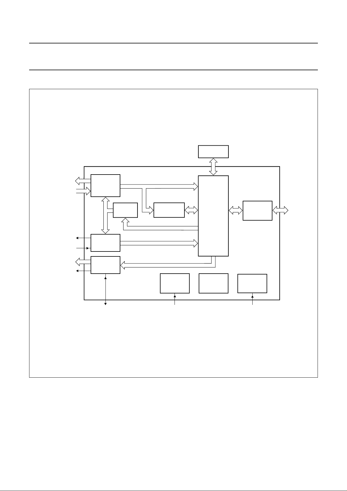
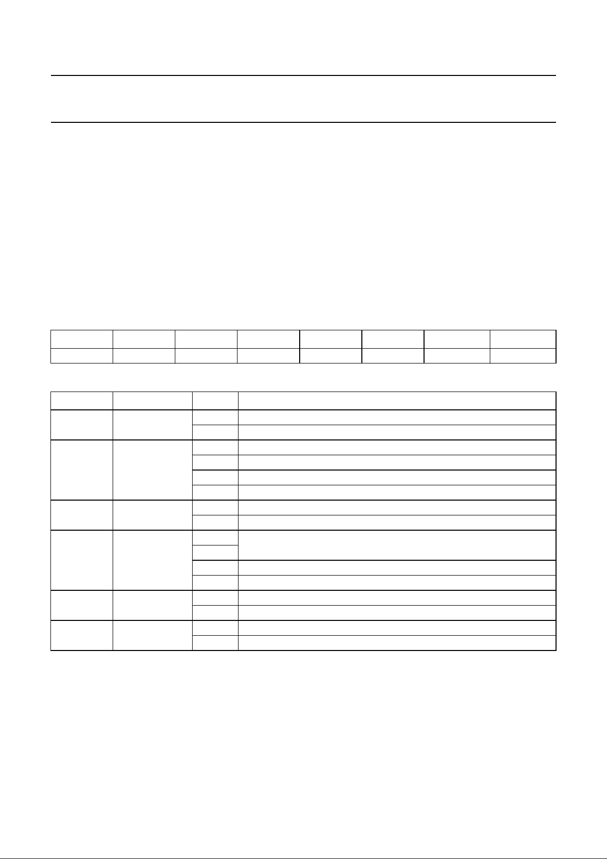
5 BLOCK DIAGRAM
handbook, full pagewidth
2
I
S-bus to CD-R
2
S-bus
I
from CD-DSP
subcode to CD-R
subcode
from CD-DSP
2
S-bus to DAC
I
IEC 958
DRIVE
INTERFACE
SUBCODE
INTERFACE
MULTIMEDIA
INTERFACE
ENCODER
ERROR
CORRECTOR
SYSTEM
CLOCK
GENERATOR
clockmaster clock
EXTERNAL
DRAM
MEMORY
PROCESSOR
TEST
CONTROL
BLOCK
ATAPI
HOST
INTERFACE
SAA7391
SUB-CPU
INTERFACE
sub-CPU
IDE-bus
MGK506
Fig.1 The SAA7391 internal block diagram.
1997 Aug 01 5

Philips Semiconductors Objective specification
ATAPI CD-R block encoder/decoder SAA7391
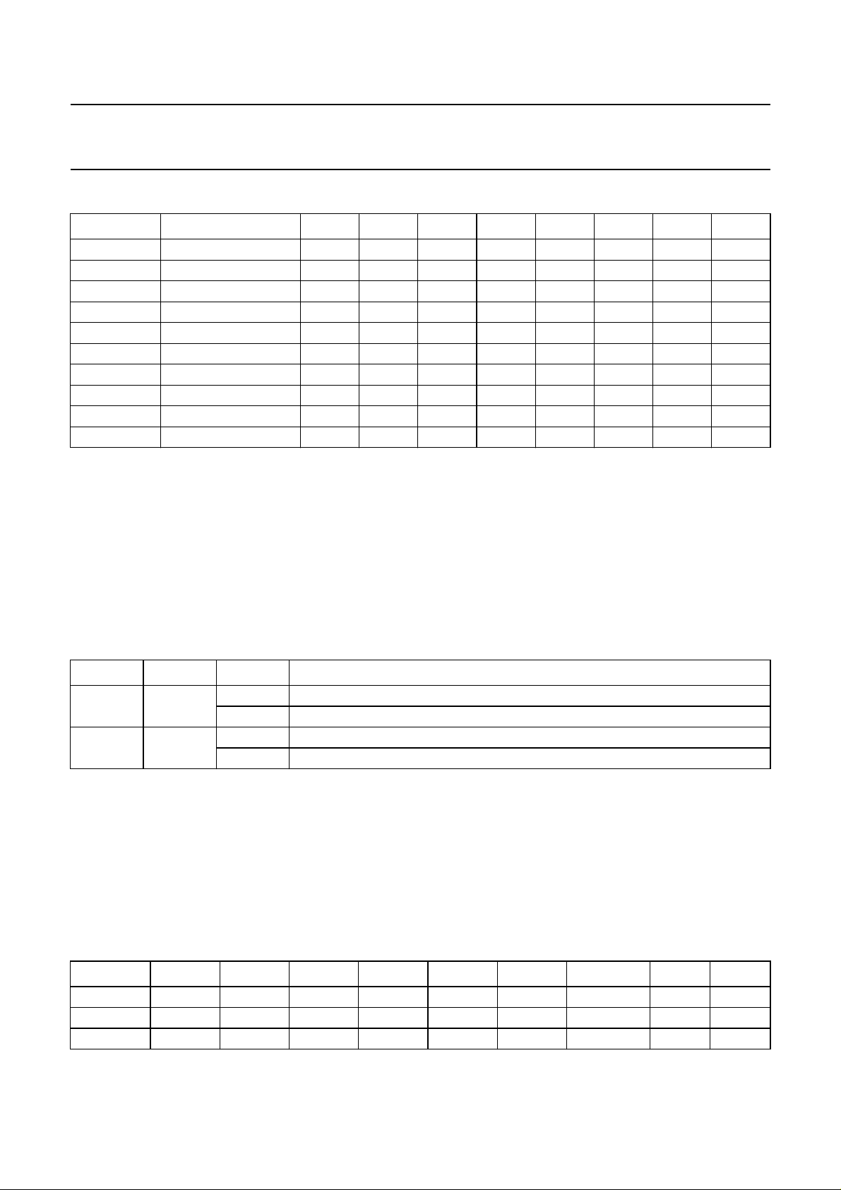
6 PINNING
SYMBOL PIN TYPE
DRIVE/
THRESHOLD
GROUPING DESCRIPTION
n.c. 1 −− −not connected
n.c. 2 −− −not connected
XDA0 3 O M RAM output address lines
XDA1 4 O M
XDA2 5 O M
V
DDD(pad6)
6 −− −digital peripheral supply voltage 6
DGND1 7 −− −digital ground 1
XDA3 8 O M RAM output address lines
XDA4 9 O M
XDA5 10 O M
XDA6 11 O M
XDA7 12 O M
XDA8 13 O M
XDA9 14 O M
XDA10 15 O M
XDA11 16 O M
DGND2 17 −− −digital ground 2
XRAS 18 O H RAM row address strobe output (active LOW)
XCAS 19 O H column address strobe output (active LOW)
XWR 20 O H write enable output (active LOW)
XDD0 21 I/O M/T RAM data bus input/output
XDD1 22 I/O M/T
V
DDD(core1)
23 −− −digital core supply voltage 1
DGND3 24 −− −digital ground 3
XDD2 25 I/O M/T RAM data bus input/output
XDD3 26 I/O M/T
XDD4 27 I/O M/T
XDD5 28 I/O M/T
XDD6 29 I/O M/T
XDD7 30 I/O M/T
V
DDD(pad7)
31 −− −digital peripheral supply voltage 7
DGND4 32 −− −digital ground 4
2
SCKI1 33 I C I
WSI1 34 I C I
S-bus I/O I2S-bus bit clock input
2
S-bus word select strobe input
1997 Aug 01 6
Philips Semiconductors Objective specification
ATAPI CD-R block encoder/decoder SAA7391
SYMBOL PIN TYPE
DRIVE/
THRESHOLD
GROUPING DESCRIPTION
n.c. 35 to 38 −− −not connected
SDI1 39 I C I
2
S-bus I/O data input from CD engine
SDO1 40 O M data output to CD-R writer
SFSY 41 I/O L/C subcode I/O 3-wire subcode sync input/output
RCK 42 I/O L/C 3-wire subcode clock input/output
SUBI 43 I C Q and R-W subcode input
SUBO 44 O L subcode output from encoder to writer
CFLG 45 I C I
2
S-bus input CD error corrector flags and absolute time
sync
C2P0 46 I C CD C2 error correction flag input for ERCO
DGND5 47 −− −digital ground 5
IECO 48 O M multimedia IEC 958 output
MCK 49 I/O M/C multimedia
output
or 384fs clock for multimedia master
256f
s
clock/IEC 958 clock or divided system clock
for CD-DSP
SCK2 50 I/O L/C multimedia I
WS2 51 I/O L/C I
SDO2 52 O M I
2
S-bus bit clock input/output
2
S-bus word select strobe input/output
2
S-bus data output to DAC/video decoder
GND 53 −− −ground
CROUT 54 O crystal pad crystal oscillator crystal oscillator output
CRIN 55 I crystal pad crystal oscillator/clock input
V
I
DDA
ref
56 −− −analog supply voltage
57 analog current input clock generator VCO reference current
POR 58 I Schmitt trigger system power-on reset (active LOW)
TEST1 59 I C test mode control input test pins
TEST2 60 I C
RESET 61 I Schmitt trigger host ATAPI bus reset input from host (active LOW)
DD7 62 I/O AL/T host data bus input/output
DD8 63 I/O AL/T
DD6 64 I/O AL/T
V
DDD(pad1)
65 −− −digital peripheral supply voltage 1
DGND6 66 −− −digital ground 6
DD9 67 I/O AL/T host data bus pin order of ATAPI interface matches
DD5 68 I/O AL/T
DD10 69 I/O AL/T
the pinning of the 40-way IDE connector (slew
rate limiting by control of drive capability into
capacitive load of ATA bus)
DD4 70 I/O AL/T
1997 Aug 01 7
Philips Semiconductors Objective specification
ATAPI CD-R block encoder/decoder SAA7391
SYMBOL PIN TYPE
DRIVE/
THRESHOLD
GROUPING DESCRIPTION
n.c. 71 to 74 −− −not connected
DD11 75 I/O AL/T host data bus; pin order of ATAPI interface
DD3 76 I/O AL/T
DD12 77 I/O AL/T
DD2 78 I/O AL/T
matches the pinning of the 40-way IDE
connector (slew rate limiting by control of
drive capability into capacitive load of
ATA bus)
DD13 79 I/O AL/T
DD1 80 I/O AL/T
DD14 81 I/O AL/T
DD0 82 I/O AL/T
DD15 83 I/O AL/T
DMARQ/
DMACK
84 O AL host DMA request/SCSI DMA acknowledge output
(active LOW)
DGND7 85 −− −digital ground 7
V
DDD(pad2)
86 −− −digital peripheral supply voltage 2
DIOW 87 I L/T host write cycle write enable/control register write
input (active LOW)
DIOR 88 I L/T host read cycle read enable/control register read
input (active LOW)
IORDY 89 O AH host device is ready to transfer data output
(active LOW)
DMACK/
DMARQ
90 I T host DMA acknowledge (active LOW)/SCSI DMA
request input
INTRQ 91 A host host interrupt request (NB 3-state output)
DGND8 92 −− −digital ground 8
V
DDD(pad3)
93 −− −digital peripheral supply voltage 3
IOCS16 94 O AH host I/O port is 16-bit output (active LOW)
DA1/
DBWR 95 I/O L/T host address wire 1/DMA from generic interface is
output from the SAA7391 (active LOW)
PDIAG 96 I/O AL/T host ATAPI passed diagnostics input/output
(active LOW)
DA0 97 I/O L/T host address wire 0 input/output
DA2/
DBRD 98 I/O L/T host address wire 2/DMA from generic interface is
input to the SAA7391 (active LOW)
CS0/
SCSICS
99 I/O L/T host chip select 1FX/generic interface chip select
(active LOW)
CS1 100 I/O L/T host chip select 3FX input/output (active LOW)
DASP 101 I/O AH/T host device active slave present input/output
(active LOW)
INT2 102 O L sub-CPU sub-CPU interrupt output from the SAA7391
drive block and UART
1997 Aug 01 8
Philips Semiconductors Objective specification
ATAPI CD-R block encoder/decoder SAA7391
SYMBOL PIN TYPE
DRIVE/
THRESHOLD
GROUPING DESCRIPTION
DGND9 103 −− −digital ground 9
V
DDD(pad4)
104 −− −digital peripheral supply voltage 4
COMACK 105 I C UART command acknowledge/transmit flow control
input
COMCLK 106 O L UART serial data clock for synchronous mode output
n.c. 107 to 110 −− −not connected
COMOUT 111 O L UART transmit data output
COMIN 112 I C UART receive data input
COMSYNC 113 I C UART basic engine synchronization input
SYSSYNC 114 I C UART basic engine synchronization input
SCCLK 115 O M sub-CPU sub-CPU clock output
RD 116 I T sub-CPU sub-CPU read enable (active LOW)
WR/R/W 117 I T sub-CPU sub-CPU write enable/and read/write control
input (active LOW)
INT 118 O L sub-CPU sub-CPU interrupt request output from host
interface (active LOW)
SRST 119 O L sub-CPU sub-CPU reset output
SCA0/SCD0 120 I/O L/T sub-CPU multiplexed address/data lines
SCA1/SCD1 121 I/O L/T
DGND10 122 −− −digital ground 10
V
DDD(pad5)
123 −− −digital peripheral supply voltage 6
SCA2/SCD2 124 I/O L/T sub-CPU multiplexed address/data lines
SCA3/SCD3 125 I/O L/T
SCA4/SCD4 126 I/O L/T
SCA5/SCD5 127 I/O L/T
SCA6/SCD6 128 I/O L/T
SCA7/SCD7 129 I/O L/T
DGND11 130 −− −digital ground 11
V
DDD(core2)
131 −− −digital core supply voltage 2
ALE 132 I T sub-CPU demultiplex enable input for lower address
lines
PSEN 133 I T sub-CPU program store enable (active LOW)
SCA15 134 I T sub-CPU upper address lines input
SCA14 135 I T
SCA13 136 I T
SCA12 137 I T
DGND12 138 −− −digital ground 12
1997 Aug 01 9
Philips Semiconductors Objective specification
ATAPI CD-R block encoder/decoder SAA7391
SYMBOL PIN TYPE
SCA11 139 I T sub-CPU upper address lines input
SCA10 140 I T
SCA9 141 I T
SCA8 142 I T
n.c. 143 −− −not connected
n.c. 144 −− −not connected
DRIVE/
THRESHOLD
GROUPING DESCRIPTION
1997 Aug 01 10

Philips Semiconductors Objective specification
ATAPI CD-R block encoder/decoder SAA7391
handbook, full pagewidth
XDA0
XDA1
XDA2
V
DDD(pad6)
DGND1
XDA3
XDA4
XDA5
XDA6
XDA7
XDA8
XDA9
XDA10
XDA11
DGND2
XRAS
XCAS
XDD0
XDD1
V
DDD(core1)
DGND3
XDD2
XDD3
XDD4
XDD5
XDD6
XDD7
V
DDD(pad7)
DGND4
SCKI1
n.c.
n.c.
XWR
WSI1
n.c.
n.c.
n.c.
n.c.
SCA8
SCA9
SCA10
SCA11
DGND12
SCA12
SCA13
SCA14
144
143
142
141
140
139
138
137
136
135
1
2
3
4
5
6
7
8
9
10
11
12
13
14
15
16
17
18
19
20
21
22
23
24
25
26
27
28
29
30
31
32
33
34
35
36
3738394041424344454647484950515253545556575859606162636465666768697071
n.c.
n.c.
SDI1
SDO1
SFSY
RCK
SUBI
SUBO
CFLG
C2P0
SCA15
PSEN
134
133
IECO
DGND5
DDD(core2)
ALE
V
132
131
MCK
SCK2
DGND11
SCA7/SCD7
130
129
SAA7391
WS2
SDO2
SCA6/SCD6
SCA5/SCD5
128
127
GND
CROUT
SCA4/SCD4
SCA3/SCD3
SCA2/SCD2
126
125
124
ref
I
DDA
CRIN
V
DDD(pad5)
V
DGND10
SCA1/SCD1
123
122
121
POR
TEST1
TEST2
SCA0/SCD0
SRST
INT
120
119
118
DD7
DD8
RESET
WR/R/WRDSCCLK
117
116
115
DD6
DGND6
DDD(pad1)
V
SYSSYNC
COMSYNC
COMIN
114
113
112
DD9
DD5
DD10
COMOUT
n.c.
n.c.
111
110
109
72
n.c.
n.c.
DD4
n.c.
108
n.c.
107
COMCLK
106
105
COMACK
V
104
DDD(pad4)
DGND9
103
INT2
102
DASP
101
CS1
100
CS0/SCICS
99
DA2/DBRD
98
DA0
97
96
PDIAG
95
DA1/DBWR
IOCS16
94
V
93
DDD(pad3)
DGND8
92
INTRQ
91
90
DMACK/DMARQ
89
IORDY
88
DIOR
87
DIOW
V
86
DDD(pad2)
DGND7
85
84
DMARQ/DMACK
DD15
83
DD0
82
DD14
81
DD1
80
DD13
79
DD2
78
DD12
77
DD3
76
DD11
75
n.c
74
n.c.
73
MGK542
Fig.2 Pin configuration.
1997 Aug 01 11
Philips Semiconductors Objective specification
ATAPI CD-R block encoder/decoder SAA7391
6.1 Detailed description of pin functions Table 1 Q and R-W input/output subcode connections (4 pins)
SYMBOL DESCRIPTION COMMENT
SFSY 3-wire subcode sync input subcode frame sync for receiving 3-wire subcode; output
subcode frame sync for transmitting 3-wire subcode
RCK 3-wire subcode clock output bit clock for receiving 3-wire subcode; input bit clock for
transmitting 3-wire subcode
SUBI Q and R-W subcode input configurable for 3-wire or Philips V4 subcode mode; can use either
RCK or WSI1 as clock references with appropriate dividers
SUBO output subcode from encode configurable for Philips SRI (Subcode Recordable Interface) 3-wire or
Philips V4 subcode mode; can use either RCK, WSI1 or WS2 as clock
references
Table 2 I
2
S-bus multimedia audio output (5 pins)
SYMBOL DESCRIPTION COMMENT
MCK 256f
multimedia master
clock/IEC 958 clock or
divided system clock for
or 384fs clock for
s
Clock reference input pin when interface is in a master mode; a
programmable divider is provided. This pin is also configurable as a
programmable clock output intended as a clock reference for a
CD-DSP. Should be pulled up if not in use.
CD-DSP
2
SCK2 I
S-bus bit clock This is used for master and slave I2S-bus application as both modes
are needed. For instance, the Philips multimedia CODEC is an I2S-bus
slave, hence this must be a master interface. When driving some
DACs, this interface can be a slave.
WS2 I
SDO2 I
2
S-bus left/right strobe word select strobe either master or slave
2
S-bus data to DAC/video
I2S-bus multimedia data
decoder
IECO IEC 958 output the IEC 958 output combines multimedia data and Q-W subcode
Table 3 I
2
S-bus connections to CD engine (6 pins)
SYMBOL DESCRIPTION COMMENT
SCKI1 I
2
S-bus bit clock this is a separate clock to the multimedia bit clock as this rate is
derived from the disc linear velocity
2
WSI1 I
SDI1 I
SDO1 I
C2P0 CD C2 error corrector flag
CFLG CD error corrector flags and
S-bus left/right strobe
2
S-bus data from CD-DSP
2
S-bus data to CD-writer
from ERCO
absolute time sync
these flags are used to indicate errors from second layer correction to
the ERCO
The absolute time sync is used in the CD input process for playing
‘Red Book’ discs; the error corrector status is also read in from this
signal, to provide an indication of C1 and C2 performance for CD-RW
applications.
1997 Aug 01 12
Philips Semiconductors Objective specification
ATAPI CD-R block encoder/decoder SAA7391
Table 4 ATAPI target mode interface
ATAPI
NAME
RESET ATAPI reset signal: the SAA7391 will not recognize a signal assertion shorter than 20 ns as a valid
reset signal.
DD0 to DD7 ATAPI D0 to D7
DD8 to DD15 ATAPI D8 to D15: these data bits are only used in accesses to the 16-bit data port
DMARQ DMA request: this signal, used for DMA data transfers between host and device, is asserted by the
SAA7391 when it is ready to transfer data to or from the host. The direction of data transfer is
controlled by
DMACK DMA acknowledge: this signal is used by the host in response to DMARQ to initiate DMA transfers.
This signal may be temporarily negated by the host to suspend the DMA transfer in process.
IOCS16 A TAPI I/O port is a 16-bit open-drain output: during PIO transfer Modes 0, 1 or 2, IOCS16 indicates to
the host system that the 16-bit data port has been addressed and that the device is prepared to send
or receive a 16-bit data word.
IORDY ATAPI I/O ready open-drain output: this signal is negated to extend the host transfer cycle of any host
register access (read or write) when the SAA7391 is not ready to respond to a data transfer request.
This signal is only enabled during DIOR/DIOW cycles to the SAA7391. When IORDY is not active, it is
in the high-impedance (undriven) state.
DA0 to DA2 address bus (device address)
DIOW ATAPI write strobe: the rising edge of DIOW latches data from the signals, DD0 to DD7 or
DD0 to DD15 into a register or the data port of the SAA7391. The SAA7391 will not act on the data
until it is latched.
DIOR ATAPI read strobe: the falling edge of DIOR enables data from a register or data port of the SAA7391
onto the signals, DD0 to DD7 or DD0 to DD15. The rising edge of DIOR latches data at the host and
the host will not act on the data until it is latched.
CS0 ATAPI chip select 0 input: this is the chip select signal from the host used to select the ATA command
block registers. This signal is also known as CS1FX.
CS1 ATAPI chip select 1 input: this is the chip select signal from the host used to select the ATA control
block registers. This signal is also known as CS3FX.
INTRQ ATAPI interrupt output: this signal is used to interrupt the host system. INTRQ is asserted only when
the device has a pending interrupt, the device is selected, and the host has cleared the ‘nien’ bit in the
device control register. If the ‘nien’ bit is equal to 1, or the device is not selected, this output is in a
high-impedance state, regardless of the presence or absence of a pending interrupt.
PDIAG ATAPI passed diagnostics: this signal shall be asserted by device 1 to indicate to device 0 that it has
completed diagnostics.
DASP ATAPI DASP (device active, device 1 present): this is a time-multiplexed signal which indicates that a
device is active, or that device 1 is present. This signal is an open-drain output.
DIOR and DIOW.
ATAPI MEANING
1997 Aug 01 13
Philips Semiconductors Objective specification
ATAPI CD-R block encoder/decoder SAA7391
Table 5 Generic host controller interface
ATAPI
NAME
RESET RESET controller reset output
DD0 to DD7 D0 to D7 controller DMA path/controller data and control bus (optional)
DD8 to DD15 D8 to D15 controller upper DMA path (optional)
DMARQ
DMACK DMARQ DMA request from controller
DA1
DA2
CS0 SCSICS controller chip select output for sub-CPU read/write cycles
Table 6 Miscellaneous pins
SYMBOL DESCRIPTION COMMENT
CRIN crystal oscillator/clock input −
CROUT crystal oscillator output −
I
ref
POR power-on reset pin −
TEST1 and TEST2 mode control test pins −
Table 7 Sub-CPU interface pins
GENERIC
INTERFACE
NAME
DMACK DMA acknowledge to controller
DBWR DMA bus write to controller
DBRD DMA bus read from controller
VCO reference current clock PLL multiplier
GENERIC HOST CONTROLLER INTERFACE MEANING
SYMBOL DESCRIPTION COMMENT
SRST sub-CPU reset active HIGH reset if XDD7 is pulled LOW during power-on reset;
active LOW reset if XDD7 is pulled HIGH during power-on reset
INT sub-CPU interrupt request
output from host interface
INT2 sub-CPU interrupt output from
the SAA7391 drive block and
UART
SCCLK sub-CPU clock out −
RD sub-CPU read enable sub-CPU read enable strobe; if grounded permanently, the WR
WR/R/W sub-CPU write enable/
read/write control
ALE demultiplex enable input for
lower address lines
open-drain sub-processor interrupt from host interface
open-drain sub-processor interrupt from drive and UART
signal will act as read/write control input
write enable; alternative usage is read/write if RD is held LOW at
all times; WR has priority over RD at all times
while HIGH, the lower address bits are latched from
SCD0 to SCD7; should be used with a Schmitt trigger input to
avoid false latching due to ground bounce on the
8051 microcontroller
1997 Aug 01 14
Philips Semiconductors Objective specification
ATAPI CD-R block encoder/decoder SAA7391
SYMBOL DESCRIPTION COMMENT
PSEN program store enable if this pin is LOW then the 8051 microcontroller is accessing
external program store; this pin is used as an active HIGH chip
enable
SCD0 to SCD7/
SCA0 to SCA7
SCA8 to SCA15 sub-CPU address high bits −
Table 8 RAM interface pins
SYMBOL DESCRIPTION COMMENT
XDA0 to XDA11 RAM address bits, multiplexed for DRAM up to 16 Mbytes DRAM only supported
XRAS DRAM row address strobe
XCAS DRAM column address strobe
XWR RAM write enable
XDD0 to XDD7 RAM data bus
sub-CPU data bus
multiplexed/low address bus
−
Table 9 Basic engine interface
SYMBOL DESCRIPTION COMMENT
SYSSYNC basic engine synchronization input generate interrupts on rising and/or falling edges
COMSYNC basic engine synchronization input generate interrupts on rising and/or falling edges
COMIN receive data −
COMOUT transmit data −
COMCLK serial data clock for synchronous mode −
COMACK command acknowledge/transmit flow
control
7 FUNCTIONAL DESCRIPTION
The SAA7391 device consists of a number of main
functional units; a CD engine interface, a multimedia block,
a microcontroller interface, an error detection and
correction block, a host interface and a memory manager.
There are also several smaller blocks including a clock
control block and a UART for communication with the CD
engine. Each block is independently controlled by a
dedicated register set. These registers are memory
mapped to the sub-CPU to allow for faster access.
The external RAM can also be accessed directly from the
microcontroller to support scratchpad accesses and thus
eliminate the need for further memory devices in the
system.
7.1 Memory field description
must be HIGH for synchronous mode to transmit
next data byte
into blocks. It then writes the blocks to the buffer memory
and onboard ERCO RAM. Any detected errors are then
corrected and over written into the buffer memory.
Memory is segmented and addressable by segment
pointers. The segment pointers consist of a block number,
offset pointer and byte number within the block. The data
within each segment is organised in the same manner
(see Table 10).
The arrangement of data within each segment in memory
differs from other Philips devices, because of the different
error correction processing possibilities within the
SAA7391.
Addresses 0 to 2355 are written to memory by the drive
processor when enabled.
The CD input function of the SAA7391 buffer manager
receives the main data stream in I
CD-DSP, performs sync detection and partitions the data
1997 Aug 01 15
2
S-bus format from the

Philips Semiconductors Objective specification
ATAPI CD-R block encoder/decoder SAA7391
Table 10 The memory map of a block in the buffer RAM for standard density mode (see Table 11)
ADDRESS (OFFSET) TYPE OF DATA
0 to 3 header field
4 to 2339 block data field
2340 to 2351 sync field
2352 copy of STAT0
2353 copy of STAT1
2354 copy of STAT2
2355 number of C2 flags in sector (compressed format)
2356 to 2451 96-byte de-interleaved R-W data field
2452 to 2463 12-byte Q-subcode field
2464 to 2465 copy of STAT4 field; only valid if ERCO did run on this block
2466 to 2559 user work space
Table 11 Description of Table 10
DATA DESCRIPTION
Header field The 4-byte header data consists of a 3-byte block address of absolute time (minutes,
seconds and frame, bytes 0 to 3). The fourth byte is for the mode of data:
Mode 0 = zero mode
Mode 1 = data storage with EDC and ECC
Mode 2 = data storage
Block data field in the CD-ROM mode the block data consists of 2048 bytes of user data and 288 bytes of
auxiliary data
User data:
Mode 0= all 2048 bytes in user data are zero
Mode 1= all 2048 bytes are available to the user
Mode 2= all 2048 bytes are available to the user
Auxiliary data:
Mode 0= all 288 bytes in Aux data are zero
Mode 1= the Aux field is in accordance with the EDC and ECC specification
Mode 2= all 288 bytes are available to the user
Sync field The 12-byte sync field is the next segment in memory. All bytes in the sync field are FFH,
except the first and last bytes which are $00.
1997 Aug 01 16

Philips Semiconductors Objective specification
ATAPI CD-R block encoder/decoder SAA7391
DATA DESCRIPTION
Number of C2 flags in
sector (compressed
format)
96-byte de-interleaved
R-W data field
12-byte Q-subcode field as above: these will not be separated out if the copy2 interleaving option is set to raw
2 copies of STAT4 field Address 2465 and 2466 are copies of the STAT4 register written by the ERCO when
While storage of C2 flag positions is not possible as a consequence of the architecture of
the SAA7391, a count of the number of flags seen per block is made in a single-byte
counter. This counter packs the possibly 12-bit count into a single byte in the following
way, at the expense of resolution in the count values for large counts.
C2count_val = count (5 down to 0) × [4 ^ count (7 down to 6)], the resolution of the count
is therefore:
C2count_val 0 to 63: counter resolution = 1
C2count_val 64 to 255: counter resolution = 4
C2count_val 256 to 1023: counter resolution = 16
C2count_val 1024 to 4095: counter resolution = 64
Written to memory by the automatic Q-channel copy process (copy2 channel). If the copy
process is not enabled, these fields are not written (see Section 7.3.5). These bytes may
either be R-W de-interleaved or presented as raw Q-W subcode bytes. If the copy2
interleaving mode is set to raw, interleaved copying is still required as the subcode
temporary holding buffer has Q bytes interspersed with the raw R-W.
enabled. This allows the user to determine if the ST AT4 register has been written to by the
ERCO. If seg2465 = seg2466 then STAT4 definitely has not been written by the ERCO.
If seg2465 ≠ seg2466 then STAT4 probably has not been written by the ERCO.
Via direct access to buffer memory, the sub-CPU will be able to look at all of the blocks so
far corrected, to check their status, in a background task.
ERCO failures do not have to be dealt with immediately, as the status of every block
loaded in to RAM is stored with that block, and it is not overwritten until the RAM block is
filled with new data from CD input.
The error corrector will be controlled additionally to permit the use of single pass P-Q or
only EDC operation to allow for greater than n = 14 operation of the ERCO.
The ERCO status will be copied into the RAM along with the data. This is possible
because the RAM now has spare capacity to store the information, as part of the change
from linear to segment/offset addressing.
It is possible to program transfers into RAM of more than one block without processor
intervention. It is also possible to continually loop on the same buffer area of RAM, by not
altering the reload register values when the reload interrupt occurs.
7.1.1 DVD-ROM MEMORY FIELD INFORMATION
The buffer arrangement for DVD usage is basically the same (data followed by flags) but the size of the block data differs,
and the ERCO flags are at a different offset, and as the ERCO is not in use, the flags relating to ERCO performance will
not be valid.
1997 Aug 01 17
Philips Semiconductors Objective specification
ATAPI CD-R block encoder/decoder SAA7391
7.2 CD input control registers
The CD input process is intended to be as automated as possible. Data is read in from the front end, descrambled if in
CD-ROM mode and then written to RAM. The registers that control the address of where the data is written to are in the
memory processor block.
The input data is synchronized, decoded and written to the buffer RAM. The input data format is software programmable.
The synchronization is performed by using a sync detector and a sync interpolator. The sync detector can detect
CD-ROM syncs and syncs from the CFLG pin, for use with Red Book, audio and for DVD. When no sync is found, it is
optionally interpolated.
After decoding, each full sector of data (2352 bytes) comprising sync, header and sub-header is written to the buffer
RAM. The R-W and Q subcode is added by a software-initiated automatic block copy process.
7.2.1 R
Table 12 IFCONFIG (write only; address FF10H) (see Table 13)
Table 13 Description of the IFCONFIG register bits
EGISTERS ASSOCIATED WITH DATA IN PROCESS
BIT 7 BIT 6 BIT 5 BIT 4 BIT 3 BIT 2 BIT 1 BIT 0
ipconfig ckdiv1 ckdiv0 subsel modulo 1 modulo 0 config swap config wclk
BIT NAME VALUE MEANING
7 ipconfig 0 I
1 EIAJ serial interface mode
6 and 5 ckdiv1 and
ckdiv0
4 subsel 0 both copies of sub-header contribute to STAT1/sh0errtosh3err
3 and 2 modulo 1 and
modulo 0
1 config swap 0 the received data from the CD-DSP or drive FIFO is not swapped
0 config wclk 0 the internal ‘irclk’ is not inverted
00 oversample, bit clock division ratio = 2
01 oversample, bit clock division ratio = 4
10 oversample, bit clock division ratio = 8
11 bit clock division ratio = 1 (no division)
1 first copy only of sub-header contributes to STAT1/sh0err to sh3err
00 modulo count 2352
01
10 modulo count 2064
11 modulo count 2064, but do not count bytes with flag = 1
1 the received data from the CD-DSP or drive FIFO is swapped
1 the internal ‘irclk’ is inverted
2
S-bus mode
1997 Aug 01 18
Philips Semiconductors Objective specification
ATAPI CD-R block encoder/decoder SAA7391
Table 14 CD input control registers (see Table 15)
ADDRESS NAME BIT 7 BIT 6 BIT 5 BIT 4 BIT 3 BIT 2 BIT 1 BIT 0
FF21H DRIVECURSEG-L s7 s6 s5 s4 s3 s2 s1 s0
FF20H DRIVECURSEG-H incen wren − s12 s11 s10 s9 s8
FF60H DRIVECURCOUNT c7 c6 c5 c4 c3 c2 c1 c0
FF27H DRIVENEXTSEG-L s7 s6 s5 s4 s3 s2 s1 s0
FF26H DRIVENEXTSEG-H incen wren − s12 s11 s10 s9 s8
FF61H DRIVENEXTCOUNT c7 c6 c5 c4 c3 c2 c1 c0
FF23H DRIVEPREVSEG-L s7 s6 s5 s4 s3 s2 s1 s0
FF22H DRIVEPREVSEG-H incen wren − s12 s11 s10 s9 s8
FF24H DRIVEOFFSET-H s7 s6 s5 s4 s3 s2 s1 s0
FF25H DRIVEOFFSET-L s7 s6 s5 s4 s3 s2 s1 s0
There are two sets of address registers, one giving the current (DRIVECURSEG) number of the segment being filled and
a segment/block counter. The other set contains the values (DRIVENEXTSEG) to use on completion of the current group
of blocks being filled or emptied (in CD-R). The DRIVEPREVSEG register is loaded with the value of the DRIVECURSEG
register at the end of each CD-ROM block.
The reloading of the registers will trigger an interrupt, if enabled, of the sub-CPU, which will then have to reload the ‘next’
registers. before the transfer requested in the ‘current’ registers are exhausted.
Memory is split into segments, each segment is 2560 bytes. The drive data is written one block at a time at the segment
number pointed to by the DRIVECURSEG register. For the next block the ‘DRIVECURSEG’ is updated as follows.
Table 15 Description of the ‘incen’ and ‘wren’ bits (see Table 14)
BIT NAME VALUE MEANING
(2)
(1)
0 hold value of DRIVECURSEG
1 increment DRIVECURSEG at the end of each CD-ROM block received
0 enable writes of data transferred
1 disable write of data transferred
7 incen
6 wren
Notes
1. If ‘incen’ is logic 1, the ‘DRIVECURSEG’ pointer will increment every sector sync. The ‘DRIVECURCOUNT’ will
decrement every sector sync independent of ‘incen’. If ‘incen’ is logic 0 then the pointer will remain fixed pointing at
the same segment of RAM. If the reading of data from CD is enabled by the ‘wrreq’ bit in the CTRL0 register, and
the ‘wren’ bit is logic 0 the segment will be repeatedly filled by the data coming in from the CD-ROM.
2. If ‘wren’ is logic 1 and ‘incen’ is logic 1 then the DRIVECURSEG register will increment with each sync time and the
DRIVECURCOUNT register will decrement but data will not be written to external RAM. This allows the triggering of
the reading of data or the writing of data some time in the future.
Table 16 Control and status registers (see Tables 17, 18 and 19)
ADDRESS NAME BIT 7 BIT 6 BIT 5 BIT 4 BIT 3 BIT 2 BIT 1 BIT 0
FF0DH CTRL0 decen ahead e01rq autoform eramrq wrreq eccrq encode
FF0EH CTRL1 syien syden asyn cowren onepass − − −
FF0FH CTRL2 modrq formrq − automode mbckrq − dscren −
1997 Aug 01 19

Philips Semiconductors Objective specification
ATAPI CD-R block encoder/decoder SAA7391
Table 17 Description of the CTRL0 register bits (resetting the chip sets all the bits in this register to 0)
BIT NAME VALUE DESCRIPTION
2
7 decen 0 disable decoding, drive in ‘full reset’ state, no monitor of I
interrupts
1 enable decoding
6 ahead 0 obsolete
1 must be set to logic 1
5 e01rq 0 disable error correction of bytes for which an error has been detected, but not
yet corrected
1 enable CRC miscorrection correction of the C2 flag bytes
4 autoform 0 disable automatic Form detection
1 enable automatic Form detection
3 eramrq 0 disable erasure flag use
1 enable erasure flag use
2 wrreq 0 disable data writes to the buffer and pointer updates, only header and status
information recovered
1 enables data writes to the buffer and pointer updates
1 eccrq 0 disable ECC correction only EDC checking
1 enable ECC correction, ERCO active
0 encode 0 read operation
1 perform erasure correction on P and Q check symbols, resulting in encoder
operation
S-bus line, no
Table 18 Description of the CTRL1 register bits (the reset function clears all the flags in this register)
BIT NAME VALUE DESCRIPTION
7 syien 0 disable sync interpolation
1 enable sync interpolation
6 syden 0 disable sync detection
1 enable sync detection
5 asyn 0 CD-ROM sync detection
1 audio sync detection
4 cowren 0 disable rewriting of corrected error bytes
1 enable rewriting of error bytes during error correction
3 onepass 0 normal error corrector operation
1 one pass only error correction
1997 Aug 01 20
Philips Semiconductors Objective specification
ATAPI CD-R block encoder/decoder SAA7391
Table 19 Description of the CTRL2 register bits
BIT NAME VALUE DESCRIPTION
7 modrq 0 Mode 1 request
1 Mode 2 request
6 formrq 0 Form 1 request
1 Form 2 request
4 automode 0 disable automatic determination of mode bit
1 enable automatic determination of mode bit
3 mbckrq 0 disable mode check function
1 enable mode check function
1 dscren 0 disable descrambling function
1 enable descrambling function
Table 20 Sub-CPU registers during read (see Tables 21, 22, 23, 27 and 28)
ADDRESS NAME BIT 7 BIT 6 BIT 5 BIT 4 BIT 3 BIT 2 BIT 1 BIT 0
FF00H HEAD0 minutes
FF01H HEAD1 seconds
FF02H HEAD2 frames
FF03H HEAD3 mode
FF04H SUBHEAD0 file number
FF05H SUBHEAD1 channel number
FF06H SUBHEAD2 submode
FF07H SUBHEAD3 coding Information
FF08H STAT0 − ilsync nosyn lblk − sblk erablk −
FF09H STAT1 minerr secerr blkerr moderr sh0err sh1err sh2err sh3err
FF0AH STAT2 rmod3 rmod2 rmod1 rmod0 mode form rform1 rform2
FF0BH STAT3 valst − − − − − − −
FF0CH STAT4 crcok cblk uceblk − nocor mode form qok
Table 21 Description of the STAT0 register bits (resetting the chip clears all bits in this register)
BIT NAME VALUE DESCRIPTION
7 −−reserved
− reserved
6 ilsync 0 −
1 sync pattern detected at word count 0 to 1174
5 nosyn 0 −
1 sync pattern inserted by sync interpolator not coincident with data sync
4 lblk 0 −
1 with ‘syien’ at logic 0, no sync found; data block size has been extended
3 −−reserved
− reserved
1997 Aug 01 21

Philips Semiconductors Objective specification
ATAPI CD-R block encoder/decoder SAA7391
BIT NAME VALUE DESCRIPTION
2 sblk 0 −
1 short block indication
1 erablk 0 −
1 one or more bytes of the block are flagged with C2 flags
0 −−reserved
− reserved
Table 22 Description of the STAT1 register bits; address FF09H (see notes 1 and 2)
BIT 7 BIT 6 BIT 5 BIT 4 BIT 3 BIT 2 BIT 1 BIT 0
(3)
minerr
Notes
1. Resetting the chip clears all bits in this register.
2. The bits in this register indicate the reliability of data in the HEAD0 to HEAD3 and SUBHEAD0 to SUBHEAD3
registers.
3. Bits ‘minerr’, ‘secerr’, ‘blkerr’ and ‘moderr’ indicate errors in the minutes, seconds, frames and mode bytes in the
header of the current block.
4. Bits ‘sh0err’ to ‘sh3err’ indicate errors in the respective bytes in the subheader.
secerr
(3)
blkerr
(3)
moderr
(3)
sh0err
(4)
sh1err
(4)
sh2err
(4)
sh3err
(4)
Table 23 Description of the STAT2 register bits; address FF0AH (see Tables 24, 25 and 26)
BIT 7 BIT 6 BIT 5 BIT 4 BIT 3 BIT 2 BIT 1 BIT 0
rmod3 rmod2 rmod1 rmod0 mode form rform1 rform2
Table 24 Description of the ‘mode’ and ‘form’ bits
mode form SETTING
0 0 Mode 1
1 0 Mode 2, Form 1
X 1 Mode 2, Form 2 or ECC correction impossible
Table 25 Description of the ‘rform’ bits
rform1 rform2 MEANING
0 0 Form 1
0 1 Form 2
1 X error in Form byte
1997 Aug 01 22
Philips Semiconductors Objective specification
ATAPI CD-R block encoder/decoder SAA7391
Table 26 Description of the ‘rmod’ bits
rmod3 to rmod30
0000 mode 0
0001 mode 1
0010 mode 2
0011 mode 3
0100 mode 4
0101 mode 5
0110 mode 6
0111 mode 7
1XXX packet written CD-R, run in/run out, link, XXX is mode
1111 mode = 7 or error in mode byte
Note
1. rmod3 = bit 7 #, bit 6 #, bit 5 #, bit 4 #, bit 3 # of C2P0 (where # is logic OR). This is non-zero for packet written
CD-R.
rmod2 = bit 2 # CFLG.
rmod1 = bit 1 # CFLG.
rmod0 = bit 0 # CFLG.
(1)
MEANING
Table 27 Description of the STAT3 register bit
BIT NAME VALUE DESCRIPTION
7 valst 0 registers associated with decoder interrupt valid
1 registers invalid
Table 28 Description of the STAT4 register bits (this register contains the interrupt status on reading)
BIT NAME VALUE DESCRIPTION
7 crcok 0 −
1 cyclic redundancy check OK
6 cblk 0 −
1 there has been an error in this block
5 uceblk 0 −
1 uncorrectable errors in block
4 − 0 reserved
1 reserved
3 nocor 0 −
1 ERCO was not started on this block
2 mode 0 Mode 1 used in correcting this block
1 Mode 2 used in correcting this block
1 form 0 Form 1 used in correcting this block
1 Form 2 used in correcting this block
0 qok 0 Q channel CRC no error
1 Q channel CRC error
1997 Aug 01 23

Philips Semiconductors Objective specification
ATAPI CD-R block encoder/decoder SAA7391
Table 29 Auxiliary segment pointer
ADDRESS NAME BIT 7 BIT 6 BIT 5 BIT 4 BIT 3 BIT 2 BIT 1 BIT 0
FF29H AUXSEGMENT-L s7 s6 s5 s4 s3 s2 s1 s0
FF28H AUXSEGMENT-H − − − s12 s11 s10 s9 s8
The auxiliary segment pointer points at a group of
segments which hold the data FIFOs used in the
SAA7391. These are the ‘large’ FIFOs rather than the
small resynchronizing FIFOs inside the SAA7391.
The subcode input/output and n = 1 I2S-bus interfaces use
these FIFOs (in addition, the shadow debug registers can
use some of this space).
The FIFOs are arranged to optimally occupy a contiguous
group of segments in the external RAM.
7.3 Multimedia output interface
This block deals with subcode input and output in addition
to an audio output which is independent of the I
2
S-bus
input output path connected to the CD-R engine.
Q and R-W subcode features:
• Supports semiautomatic de-interleaving/interleaving
• Subcode sync is aligned with the start of the current
block in RAM
• Supports subcode resynchronization when subcode
sync is lost
• Supports Philips ‘V4’ and 3-wire formats (only one RCK
and one SFSY pin shared with subcode output)
• Has selectable polarity on RCK
• Uses WSI1 pin as timing reference
• Can insert ‘P’ bit in 3-wire mode via sub-CPU accessible
register bit
• Supports regeneration of subcode from IEC 958 output
using WS2 as timing reference
• Can accept subcode input while I2S-bus from CD-DSP
is oversampled audio at n = 2 or n = 4 oversample
• Subcode for CD-recordable applications is supported in
Philips V4 or 3-wire Philips Subcode Recordable
Interface (SRI). This SRI mode is only compatible with
CDR60.
Audio output (multimedia) features:
• Has data output for simple audio or digital video for
n = 1 or n = 2 rate regardless of input CD-DSP data rate
• 4096-byte FIFO for audio samples, requires firmware
polling for refills using the block copy engine
• Permits CAV and quasi-CLV systems to maintain n = 1
audio output
• Basic channel swap, mono-L or mono-R modes,
includes muting and L + R summed mono
• IEC 958 output with subcode Q-W for use in CAV and
other modes where there is no n = 1 clock in the
CD-DSP subsystem
– IEC 958 interface has fully programmable category
code and copyright bits for flexibility
– Subcode on IEC 958 is only available in CD-ROM
mode, because the subcode output FIFO is shared.
2
• Master and slave I
S-bus modes are available
– IEC 958 is only available when the I2S-bus is in the
master mode.
• Can be configured to provide a clock for an external
CD-DSP function via the MCK pin
• Can operate in 64fs or 48fs I2S-bus modes
• IEC 958 can operate at n = 2 although not permitted by
standard.
7.3.1 S
UBCODE INPUT BLOCK
7.3.1.1 Q-W subcode handling
The subcode data is initially converted from
serial-to-parallel format and is then handled as Q-W bytes.
The de-interleaving is performed by a de-interleaving
block copy mode in the memory processor’s block copy
engine. Subcode blocks will always be aligned with a block
of CD-ROM data, although the subcode Minutes,
Seconds, Frames (MSF) absolute time may have an
uncertainty of ±5 frames in terms of the actual CD-ROM
block it is referring to. This offset is unknown but consistent
in any given application. The block copy engine will be
automatically triggered when the subcode synchronization
is found.
The error corrector will then compute the CRC syndrome
of the subcode and deposit it in the CRC bytes.
The sub-CPU will have to perform the actual correction if a
non-zero syndrome appears.
This syndrome, if calculated during encoding by the
ERCO, can be used as the CRC written to disc for the
subcode.
1997 Aug 01 24
Philips Semiconductors Objective specification
ATAPI CD-R block encoder/decoder SAA7391
7.3.1.2 Description of subcode interface
The subcode interface allows the reception and transmission of subcodes. The subcodes will be received/transmitted to
two on-chip 512-byte FIFOs, one for transmit and one for receive. No interrupts are associated with these FIFOs as the
block copy engine removes data or fills these as necessary.
There is, however, an interrupt which is asserted when a sync is found in an unexpected location.
7.3.2 S
Table 30 Subcode mode transmit control register (SUBMODETX; address FF13H); see Table 31
Table 31 Description of the SUBMODETX register bits
Note
1. Philips V4 subcode transmit mode must be selected for correct insertion of subcode into the IEC 958 data stream.
For CD-recordable applications with CDR60 the Philips SRI subcode mode allows for correct subcode frame
synchronization between the SAA7391 and the CDR60 device before recording commences.
Table 32 Subcode mode receive control register (SUBMODERX, address FF17H); see Table 33
UBCODE MODE TRANSMIT CONTROL REGISTER
BIT 7 BIT 6 BIT 5 BIT 4 BIT 3 BIT 2 BIT 1 BIT 0
− − − pbit − txena − V4
BIT NAME VALUE DESCRIPTION
4 pbit 0 P bit logic 1 in 3-wire mode (default)
1 P bit logic 0 in 3-wire mode
2 txena 0 subcode transmit interface is disabled
1 subcode transmit interface is enabled
0 V4 0 Philips SRI 3-wire subcode
1 Philips V4 mode; note 1
BIT 7 BIT 6 BIT 5 BIT 4 BIT 3 BIT 2 BIT 1 BIT 0
− − − wsdiv1 wsdiv0 rxena rckinvrx rxsubqw
Table 33 Description of the SUBMODERX register bits
BIT NAME VALUE DESCRIPTION
4 wsdiv1 00 no oversampling (normal CD-ROM modes)
01 2 times oversampling
3 wsdiv0 10 4 times oversampling
11 8 times oversampling
2 rxena 0 subcode receive interface is disabled
1 subcode receive interface is enabled
1 rckinvrx 0 normal RCK output
1 invert the RCK output
0 rxsubqw 0 3-wire subcode
1 Philips V4 mode (sub Q-W)
1997 Aug 01 25
Philips Semiconductors Objective specification
ATAPI CD-R block encoder/decoder SAA7391
Table 34 Subcode general (input/output pointers)
ADDRESS NAME BIT 7 BIT 6 BIT 5 BIT 4 BIT 3 BIT 2 BIT 1 BIT 0
FF2BH SUBPOINTR-L s7 s6 s5 s4 s3 s2 s1 s0
FF2AH SUBPOINTR-H − − − − − − − s8
FF2FH SUBPOINTW-L s7 s6 s5 s4 s3 s2 s1 s0
FF2EH SUBPOINTW-H − − − − − − − s8
FF2DH SUBBASEPOINTR-L s7 s6 s5 s4 s3 s2 s1 s0
FF2CH SUBBASEPOINTR-H − − − − − − − s8
FF31H SUBBASEPOINTW-L s7 s6 s5 s4 s3 s2 s1 s0
FF30H SUBBASEPOINTW-H − − − − − − − s8
7.3.2.1 Subcode buffering
The subcode is buffered in the AUXSEGMENT register. Two offset pointers, SUBPOINTR-L and SUBPOINTR-H, and
SUBPOINTW-L and SUBPOINTW-H are associated with it. The R pointer is for the subcode output and the W pointer
for the subcode input.
Pointers are also provided to point at the offset into the AUXSEGMENT register where the start of a subcode frame will
be found, SUBBASEPOINTR-L and SUBBASEPOINTR-H and SUBBASEPOINTW-L and SUBBASEPOINTW-H. The
block copy engine is expected to use these to automatically move the subcode into the segment pointed at by
DRIVECURSEG register.
7.3.3 G
ENERAL DESCRIPTION OF THE MULTIMEDIA OUTPUT INTERFACE
Table 35 Multimedia output interface register bits
ADDRESS NAME BIT 7 BIT 6 BIT 5 BIT 4 BIT 3 BIT 2 BIT 1 BIT 0
FF32H CDDA-H − − − − − − a9 a8
FF33H CDDA-L a7 a6 a5 a4 a3 a2 a1 a0
FF34H DAOFFSET-H − − − − a11 a10 a9 a8
FF35H DAOFFSET-L a7 a6 a5 a4 a3 a2 a1 a0
FF16H MMCTRL
FF70H IECCTRL
(1)
(2)
mmdiv spdx2 wslen mcksel
iecen data copyright preem vbit − accu
FF71H IECCAT cat7 cat6 cat5 cat4 cat3 cat2 cat1 cat0
FF14H MMAUD
FF15H MCK_CON
(3)
(4)
daen eiaj master − leftmode rightmode
− − − − mckxtal mckoe div
Notes
1. See Table 36.
2. See Table 39.
3. See Table 38.
4. See Table 41.
1997 Aug 01 26
Philips Semiconductors Objective specification
ATAPI CD-R block encoder/decoder SAA7391
7.3.3.1 Basic description of the multimedia output interface
The multimedia data output may be used either with an internal clock or an externally provided clock. The clock used
should be a correct multiple of 44100 Hz in order for the block to correctly output IEC 958.
The multimedia interface data FIFO is located in the block of segments associated with AUXSEGMENT master/slave
mode operation (see Fig.3).
handbook, full pagewidth
e.g. DAC
SAA7391
SCK
WS
SDO2
slave: master = 0
e.g. DAC
SCK
WS
SDO2
master: master = 1
Fig.3 Master/slave mode operation.
Table 36 Description of the MMCTRL register bits
BIT NAME VALUE DESCRIPTION
7 mmdiv − see Table 37
6 −
5 −
4 −
3 spdx2 0 I
1I
2 wslen 0 I
1I
2
S-bus output is single speed
2
S-bus (and IEC 958) output is double speed; video applications
2
S-bus bit clock is 64 times the sample rate
2
S-bus bit clock is 48 times the sample rate
1 and 0 mcksel 00 multimedia internal clock is CRIN pin
01 multimedia internal clock is MCK pin
10 multimedia internal clock is system clock
SAA7391
MGK513
1997 Aug 01 27
Philips Semiconductors Objective specification
ATAPI CD-R block encoder/decoder SAA7391
Table 37 mmdiv/mcksel relationship to clocks needed for I2S-bus and IEC 958
2
S-BUS OUTPUT
I
2
DIVIDER CODE
mmdiv
0000 48f
0001 64f
0010 96f
0011 128f
0100 192f
0101 256f
0110 384f
0111 512f
1000 768f
1001 1024f
1010 1536f
MULTIMEDIA
CLOCK
OVERSAMPLE
s
s
s
s
s
s
s
s
s
s
s
mcksel
S-BUS,
I
48 BITS PER
SAMPLE
FREQUENCY
(Hz)
2116800 1
n=1 n=2 n=1 n=2 n=1 (n=2)
(1)
− − − − −
2822400 − − 1
4233600 2 1
(1)
5644800 − − 2 1
8467200 4 2 3 1.5
11289600 − − 4 2 2 (1)
16934400 8 4 6 3 3 (1.5)
22579200 − − 8 4 4 (2)
33868800 16 8 12 6 6 (3)
45158400 − − 16 8 8 (4)
67737600 32 16 24 12 12 (6)
I2S-BUS,
64 BITS PER
SAMPLE
(1)
(1)
1.5
IEC 958
− − −
− − −
(1)
(1)
1 −
1.5 −
(2)
Notes
1. For these combinations the duty factor of the output SCK2 clock is not necessarily 50%. These combinations are
therefore not recommended.
2. This is illegal but possible.
Table 38 Description of the MMAUD register control bits
BIT NAME VALUE DESCRIPTION
7 daen
(1)
0 CD-DA interface is off
1 CD-DA Interface is on
2
6 eiaj 0 I
S-bus serial mode
1 EIAJ16 serial mode
5 master 0 I
1I
3 leftmode 00 I
01 I
210I
2
S-bus is slave
2
S-bus is master
2
S-bus left channel output is left (default)
2
S-bus left channel output is right
2
S-bus left channel output is muted
11 reserved
2
1 rightmode 00 I
S-bus right channel output is right (default). This is the opposite default to
left channel.
01 I
010I
2
S-bus right channel output is left
2
S-bus right channel output is muted
11 reserved
Note
1. If enabled, data is written to the CDDA interface from a FIFO located in the CDDA register space. If either ‘daen’ = 1
or ‘iecen’ = 1 (ieccrtl), the interface will become active.
1997 Aug 01 28
Philips Semiconductors Objective specification
ATAPI CD-R block encoder/decoder SAA7391
7.3.4 IEC 958/EBU OUTPUT
Table 39 Description of the IECCTRL register control bits (notes 1 and 2)
BIT NAME VALUE DESCRIPTION
7 iecen 0 IEC 958 interface is off
1 IEC 958 Interface is on
6 data 0 IEC 958 contains audio information
1 IEC 958 contains data
5 copyright 0 IEC 958 C bit in system channel is logic 0
1 IEC 958 C bit in system channel is logic 1
4 preem 0 audio pre-emphasis off/IEC 958 contains data
1 audio pre-emphasis on (only appears in IEC 958 C channel; de-emphasis bit is not
implemented in the SAA7391)
3 vbit 0 audio samples suitable for conversion
1 mute audio, or signal is data and should not be digital-to-analog converted at any
time
2 −−reserved
− reserved
1 to 0 accu 00 level II clock accuracy
01 level III clock accuracy (depends on mck/system clock)
10 reserved
11 reserved
Notes
1. In order for the IEC interface to operate correctly, it will require a clock at 128fs to be present.
2. The ‘vbit’ is copied into the V bit of the IEC 958 frame.
Table 40 IEC 958 system channel bit mapping (note 1)
BIT NUMBER
+0 +1 +2 +3 +4 +5 +6 +7
0 0 data copyright preem − 000
8 cat0 cat1 cat2 cat3 cat4 cat5 cat6 cat7
16 00000000
24 0000accu0 accu1 0 0
Note
1. The C bit is updated on an IEC frame-by-frame basis, the bit offset corresponds to the IEC frame offset. They are
repeated for both left and right channels. Bit 0 is present in the C bit of the first sample pair of the IEC superframe of
192 sample pairs.
BIT OFFSET
1997 Aug 01 29
Philips Semiconductors Objective specification
ATAPI CD-R block encoder/decoder SAA7391
Table 41 Description of the MCK_CON register bits (note 1)
BIT NAME VALUE DESCRIPTION
3 mckxtal 0 MCK reference is system clock (default)
1 MCK reference is the CRIN pin
2 mckoe 0 MCK pin is 3-state, an input to the MM block (default)
1 MCK pin is output
1 and 0 div 00 MCK reference is divided by 2 (default)
01 MCK reference is divided by 1.5
10 MCK reference is divided by 1
11 MCK reference is divided by 4
Note
1. The bits in this register control the use of the MCK pin as an output to clock a CD-DSP. The division ratios chosen
are suitable for the SAA7335 or CDR60 devices. If the MCK pin is not being used then it should be pulled HIGH for
correct selection of the internal multimedia clocks.
7.3.5 MEMORY-TO-MEMORY BLOCK COPY FUNCTION
This function is provided for the user to move and copy
blocks of RAM. Two pointer sets are provided. The second
of these is for the semi-automatic subcode copying
function of the subcode in the block. It is independent of
the first copy register set, which is available for e.g. audio
copying needed in the PLAY AUDIO function with the
SAA7391, and for subcode copying when recording.
When started, the copy process will copy the
COPYCOUNT register bytes from the ‘FROM’ pointers to
the ‘TO’ pointers. A copying process may be stopped
during its operation by writing to the ‘copyend’ bit.
7.3.5.1 Automatic copying of received
subcode-to-data block
When enabled, the newly received subcode will be
automatically transferred to the current host segment in
RAM.
The only register that is user programmable in the subcode
copying engine is the COPYFROM2OFFSET pointer.
The ‘COPYFROM2OFFSET’ pointer is set up by the
sub-CPU to point into the subcode input FIFO. It points at
the first byte of subcode to be copied into the current host
data block. Once triggered, this copy is automatically
set-up to correctly transfer the next block of subcode
correctly without host intervention.
Copying of the subcode in the opposite direction is
performed by the sub-CPU commanding an interleaved
copy of data using the user block copy registers. This does
not have to be as fast as the recorder function is only
specified to n ≥ 8. Hence it is not automated.
1997 Aug 01 30
 Loading...