

Philips saa7385 DATASHEETS

INTEGRATED CIRCUITS
DATA SH EET
SAA7385
Error correction and host interface
IC for CD-ROM (SEQUOIA)
Preliminary specification
File under Integrated Circuits, IC01
1996 Jun 19

Philips Semiconductors Preliminary specification
Error correction and host interface IC
for CD-ROM (SEQUOIA)
CONTENTS
1 FEATURES
1.1 General
1.2 53CF94 SCSI controller
1.3 80C32 high-speed microcontroller
1.4 Front-end interface logic
1.5 Buffer controller
1.6 Hardware third-level error correction
1.7 Additional product support
2 GENERAL DESCRIPTION
3 QUICK REFERENCE DATA
4 ORDERING INFORMATION
5 BLOCK DIAGRAM
6 PINNING
7 FUNCTIONAL DESCRIPTION
7.1 80C32 microcontroller
7.2 53CF94 fast SCSI controller
7.3 Input clock doubler
7.4 Front-end
8 MICROCONTROLLER INTERFACE
8.1 Microcontroller interface status register
8.2 Microcontroller interface command register
8.3 Microcontroller interrupts
8.4 Microcontroller RAM organization
9 FRONT PANEL AND MISCELLANEOUS
CONTROL SIGNALS
9.1 S2B UART registers
9.2 Miscellaneous control registers
10 FRONT-END
10.1 Minute Second Frame (MSF) addressing and
header information
10.2 Front-end status and control
SAA7385
11 BUFFER MANAGER
11.1 Front-end to buffer manager interface
11.2 Microcontroller to buffer manager interface
11.3 ECC to buffer manager interface
11.4 SCSI to buffer manager interface
11.5 Miscellaneous buffer manager considerations
11.6 53CF94 related registers
12 FRAME BUFFER ORGANIZATION
13 SUMMARY OF CONTROL REGISTER MAP
14 LIMITING VALUES
15 OPERATING CHARACTERISTICS
15.1 I2S-bus timing; data mode
15.2 EIAJ timing; audio mode
15.3 R-W timing (see Fig.15)
15.4 C-flag timing (see Fig.16)
15.5 S2B interface timing
15.6 SCSI interface timing
15.7 Microprocessor interface
15.8 DRAM interface (the SAA7385 is designed to
operate with standard 70 ns DRAMs)
16 PACKAGE OUTLINE
17 SOLDERING
17.1 Introduction
17.2 Reflow soldering
17.3 Wave soldering
17.4 Repairing soldered joints
18 DEFINITIONS
19 LIFE SUPPORT APPLICATIONS
1996 Jun 19 2

Philips Semiconductors Preliminary specification
Error correction and host interface IC for
CD-ROM (SEQUOIA)
1 FEATURES
1.1 General
• Single chip digital solution for an 8 × speed CD-ROM
controller chip
• 10 Mbytes/s NCR53CF94 equivalent SCSI controller
included
• High-speed 80C32 microcontroller with 256 × 8
scratch-pad SRAM included
• High performance CD-ROM interface logic
• 128 pin QFP package.
1.2 53CF94 SCSI controller
• Separate clock input to allow operation up to the
maximum 10 Mbytes/s
• Fast synchronous SCSI-2 compatible
• 24-bit transfer counter for single transfers up to
16 Mbytes
• High-speed 16-bit DMA interface to the buffer manager
DRAM
• On-chip 48 mA SCSI drivers
• Software compatible with members of the 53C90 family
• Allows for SCAM support.
SAA7385
1.5 Buffer controller
• Ten level arbitration logic
• Utilizes low cost 70 ns DRAMs
• Page mode DRAM access for high-speed error
correction and SCSI data transfer
• Data organization by 3 kbyte frames
• 256 kbyte or 1 Mbyte DRAM supported.
1.6 Hardware third-level error correction
• Third-level correction provides superior performance in
unfavourable conditions
• Full hardware error correction to reduce microcontroller
overhead
• Corrections are automatically written to the DRAM
frame buffer.
1.7 Additional product support
• All control registers mapped into 80C32 special function
memory space
• Dedicated S2B interface UART
• Input clock synthesizer
• Red book audio pass through.
1.3 80C32 high-speed microcontroller
• 33.87 MHz full system speed operation
• Three timers/event counters
• Programmable full duplex serial channel
• Eight general purpose microcontroller I/O pins
• External program ROM.
1.4 Front-end interface logic
• Full 8 × speed hardware operation
• Block decoder
• Sector sequencer
• CRC checking of Mode 1 and Mode 2, Form 1 sectors
• 212 ms watch-dog timer
• Sub-code interface with synchronization
• C-flag interface for absolute time stamp.
2 GENERAL DESCRIPTION
The SAA7385 is a high integration ASIC that incorporates
all of the digital electronics necessary to connect a CD
decoder to a SCSI host. An 80C32 microcontroller and a
53CF94 SCSI controller are embedded in the ASIC.
The following functions are supported:
• Input clock doubler
• Block decoder
• CRC checking of Mode 1 and Mode 2, Form 1 sectors
• Red book audio pass through to SCSI
• Buffer manager
• Third-level error correction
• Sub-code and Q-channel support
• Dedicated S2B interface UART
• Embedded 80C32 microcontroller
• Embedded 53CF94 SCSI controller.
1996 Jun 19 3
Philips Semiconductors Preliminary specification
Error correction and host interface IC for
CD-ROM (SEQUOIA)
The SAA7385 uses a 33.8688 MHz clock and is capable
of accepting data at eight times (n = 8 or 1.4 Mbytes/s) the
normal CD-ROM data rate.
Third level error correction hardware is included to
improve the correction efficiency of the system. The buffer
manager hardware utilizes a ten-level arbitration unit and
can stop the clock to the microcontroller to emulate a wait
condition when necessary.
The SAA7385 comprises five major functional blocks:
• The 80C32 microcontroller is an industry standard core
• The 53CF94 is an industry standard core
• The front-end block connects to the external CD-60
based decoder and fully processes the incoming data
stream to provide bytes of data that are stored in the
external buffer
• The buffer manager block provides the address
generation and timing control for the external DRAM
buffer
• The ECC block performs the error correction functions in
hardware on the data in the DRAM buffer.
SAA7385
Supply of this Compact Disc IC does not convey an
implied license under any patent right to use this IC in
any Compact Disc application.
3 QUICK REFERENCE DATA
SYMBOL PARAMETER MIN. TYP. MAX. UNIT
V
DD
T
amb
T
stg
4 ORDERING INFORMATION
TYPE
NUMBER
SAA7385GP SQFP128 plastic quad flat package; 128 leads (lead length 1.6 mm);
digital supply voltage 4.5 5.0 5.5 V
operating ambient temperature 0 − 70 °C
storage temperature −55 − +150 °C
PACKAGE
NAME DESCRIPTION VERSION
SOT387-2
body 14 × 20 × 2.8 mm
1996 Jun 19 4
Philips Semiconductors Preliminary specification
Error correction and host interface IC for
CD-ROM (SEQUOIA)
5 BLOCK DIAGRAM
handbook, full pagewidth
DECODER
CD
data subcode
DATA
CONVERTER
AND SUB-CODE
UART
data
subcode
C-flag
256K × 8 or 1M × 8
BUFFER MANAGER
LAYERED
ERROR
CORRECTOR
DRAM BUFFER
BUFFER
MAPPER
MICROCONTROLLER INTERFACE
53CF94
SCSI
SAA7385
SCSI
interface
SERVO
PROCESSOR
S2B serial interface
80C32 MICROCONTROLLER
DEBUG UART
debug
UART
SAA7385
MGE388
64K × 8 ROM
Fig.1 Block diagram (simplified).
6 PINNING
All input, output and bidirectional signals are TTL level unless otherwise stated (Pull-Down = PD25 = 25 µA;
Pull-Up = PU25 = 25 µA, PU400 = 400 µA; Slew = S2 = 2 mA, S4 = 4 mA;
CMOS slew = CMOS S2 = CMOS 2 = 2 mA; SCSI pad = SCSI = 48 mA).
SYMBOL PIN I/O PAD DESCRIPTION
DA2 1 O S4 DRAM address bus; bit DA2
DA3 2 O S4 DRAM address bus; bit DA3
DA4 3 O S4 DRAM address bus; bit DA4
V
SS1
4 −−ground 1
DA5 5 O S4 DRAM address bus; bit DA5
DA6 6 O S4 DRAM address bus; bit DA6
DA7 7 O S4 DRAM address bus; bit DA7
DA8 8 O S4 DRAM address bus; bit DA8
DA9 9 O S4 DRAM address bus; bit DA9
V
DD1
10 −−power supply 1
1996 Jun 19 5

Philips Semiconductors Preliminary specification
Error correction and host interface IC for
CD-ROM (SEQUOIA)
SYMBOL PIN I/O PAD DESCRIPTION
RAS 11 O S4 DRAM row address section; active LOW
CAS 12 O S4 DRAM column address selection; active LOW
DWR 13 O S4 DRAM write; active LOW
DOE 14 O S4 DRAM output enable; active LOW
V
SS2
DD0 16 I/O 4 mA, Schmitt, PD25 DRAM data bus; bit DD0
DD1 17 I/O 4 mA, Schmitt, PD25 DRAM data bus; bit DD1
DD2 18 I/O 4 mA, Schmitt, PD25 DRAM data bus; bit DD2
DD3 19 I/O 4 mA, Schmitt, PD25 DRAM data bus; bit DD3
V
DD2
DD4 21 I/O 4 mA, Schmitt, PD25 DRAM data bus; bit DD4
DD5 22 I/O 4 mA, Schmitt, PD25 DRAM data bus; bit DD5
DD6 23 I/O 4 mA, Schmitt, PD25 DRAM data bus; bit DD6
DD7 24 I/O 4 mA, Schmitt, PD25 DRAM data bus; bit DD7
V
SS3
LED 26 O 24 mA, CMOS test panel LED; active LOW; WTGCTL(4)
TRAYSW 27 I Schmitt, PU25 active LOW when tray is in
EJECT 28 I Schmitt, PU25 opens tray; active LOW
LQDATA 29 O 2 mA serial data to DAC
LWCLK 30 O 2 mA word strobe to DAC
V
SS4
SCLK 32 O 2 mA data serial clock
V
SS5
SYSRES 34 O 2 mA, PU25 system reset; OR of
CFLAG 35 I Schmitt, PU400 C1 and C2 status
CPR 36 O 2 mA S2B interface ready to accept data; active LOW
SPR 37 I Schmitt S2B interface ready to send data; active LOW
SKIPFWD 38 I Schmitt, PU25 skip forwards; active LOW; RDSW(3)
SKIPBACK 39 I Schmitt, PU25 skip backwards; active LOW; RDSW(2)
SCSICLK 40 I standard SCSI interface clock
V
DD3
AD0 42 I/O S4, Schmitt microcontroller multiplexed data bus; bit AD0
AD1 43 I/O S4, Schmitt microcontroller multiplexed data bus; bit AD1
AD2 44 I/O S4, Schmitt microcontroller multiplexed data bus; bit AD2
AD3 45 I/O S4, Schmitt microcontroller multiplexed data bus; bit AD3
AD4 46 I/O S4, Schmitt microcontroller multiplexed data bus; bit AD4
AD5 47 I/O S4, Schmitt microcontroller multiplexed data bus; bit AD5
AD6 48 I/O S4, Schmitt microcontroller multiplexed data bus; bit AD6
AD7 49 I/O S4, Schmitt microcontroller multiplexed data bus; bit AD7
V
SS6
LA0 51 O CMOS S2, PU25 EPROM latched lower address; bit LA0
15 −−ground 2
20 −−power supply 2
25 −−ground 3
31 −−ground 4
33 −−ground 5
POR, SCSIRST and watch-dog timer
41 −−power supply 3
50 −−ground 6
SAA7385
1996 Jun 19 6

Philips Semiconductors Preliminary specification
Error correction and host interface IC for
SAA7385
CD-ROM (SEQUOIA)
SYMBOL PIN I/O PAD DESCRIPTION
LA1 52 O CMOS S2, PU25 EPROM latched lower address; bit LA1
LA2 53 O CMOS S2, PU25 EPROM latched lower address; bit LA2
LA3 54 O CMOS S2, PU25 EPROM latched lower address; bit LA3
V
DD4
LA4 56 O CMOS S2, PU25 EPROM latched lower address; bit LA4
LA5 57 O CMOS S2, PU25 EPROM latched lower address; bit LA5
LA6 58 O CMOS S2, PU25 EPROM latched lower address; bit LA6
LA7 59 O CMOS S2, PU25 EPROM latched lower address; bit LA7
V
SS7
A8 61 O CMOS S2, PU25 EPROM upper address; bit A8
A9 62 O CMOS S2, PU25 EPROM upper address; bit A9
A10 63 O CMOS S2, PU25 EPROM upper address; bit A10
A11 64 O CMOS S2, PU25 EPROM upper address; bit A11
A12 65 O CMOS S2, PU25 EPROM upper address; bit A12
A13 66 O CMOS S2, PU25 EPROM upper address; bit A13
A14 67 O CMOS S2, PU25 EPROM upper address; bit A14
A15 68 O CMOS S2, PU25 EPROM upper address; bit A15
PSEN 69 O CMOS 2, PU25 program store enable; active LOW
V
SS8
IO 71 I/O SCSI SCSI phase signal, active LOW
REQ 72 I/O SCSI SCSI request, active LOW
CD 73 I/O SCSI SCSI phase signal, active LOW
SEL 74 I/O SCSI SCSI select, active LOW
V
SS9
MSG 76 I/O SCSI SCSI phase signal, active LOW
ACK 77 I/O SCSI SCSI acknowledge, active LOW
BSY 78 I/O SCSI SCSI busy, active LOW
V
SS10
ATN 80 I/O SCSI output in initiator mode; input in target mode, active LOW
V
DD5
SDP 82 I/O SCSI SCSI parity, active LOW
SD7 83 I/O SCSI SCSI data bus; bit SD7
SD6 84 I/O SCSI SCSI data bus; bit SD6
SD5 85 I/O SCSI SCSI data bus; bit SD5
V
SS11
SD4 87 I/O SCSI SCSI data bus; bit SD4
SD3 88 I/O SCSI SCSI data bus; bit SD3
SD2 89 I/O SCSI SCSI data bus; bit SD2
SD1 90 I/O SCSI SCSI data bus; bit SD1
SD0 91 I/O SCSI SCSI data bus; bit SD0
V
SS12
55 −−power supply 4
60 −−ground 7
70 −−ground 8
75 −−ground 9
79 −−ground 10
81 −−power supply 5
86 −−ground 11
92 −−ground 12
1996 Jun 19 7

Philips Semiconductors Preliminary specification
Error correction and host interface IC for
SAA7385
CD-ROM (SEQUOIA)
SYMBOL PIN I/O PAD DESCRIPTION
RXS2B 93 I Schmitt, PU25 S2B interface receive
TXS2B 94 O 4 mA S2B interface transmit
TRAYIN 95 I/O 4 mA, PD25 tray extend control; active LOW (general purpose signal)
TRAYOUT 96 I/O 4 mA, PD25 tray retract control; active LOW (general purpose signal)
SCSIRST 97 I Schmitt SCSI reset, active LOW; also causes a system reset
POR 98 I CMOS power-on reset; active LOW
V
DD6
UC_PORT1.7 100 I/O CMOS 2, PU25 drive speed select; microcontroller port 1.7
RAB_MUSB 101 I/O CMOS 2, PU25 RD/WR, acknowledge; microcontroller port 1.2
NRST_SEQ 102 I/O CMOS 2, PU25 reset to engine; microcontroller port 1.5
UC_PORT1.4 103 I/O CMOS 2, PU25 general purpose microcontroller I/O port; port 1.4
UC_PORT1.3 104 I/O CMOS 2, PU25 general purpose microcontroller I/O port; port 1.3
UC_PORT1.1 105 I/O CMOS 2, PU25 general purpose microcontroller I/O port; port 1.1
HOMESW 106 I/O 2 mA, PU25 actuator sled home; active LOW; microcontroller port 1.0
PLAY 107 I Schmitt laser on and focused status; active LOW; RDSW(4)
UC_PORT1.6 108 I/O CMOS 2, PU25 general purpose microcontroller I/O port; port 1.6
V
SS13
GPI1 110 I Schmitt, PU25 general purpose input; microcontroller port 3.4
GPI2 111 I Schmitt, PU25 general purpose input; microcontroller port 3.5
KILL 112 I Schmitt, PU25 shut off audio; active LOW
TXICE 113 O 4 mA debug UART output; from 80C32 serial port
RXICE 114 I Schmitt, PU25 debug UART input; to 80C32 serial port
RXSUB 115 I Schmitt, PU25 sub-code input
V
DD7
OSCIN 117 I standard master input clock; 34 or 16 MHz
V
SS14
CLAB 119 I Schmitt clock
V
SS15
DAAB 121 I Schmitt data
WSAB 122 I Schmitt word strobe
EFAB 123 I Schmitt error flag
CLK34 124 O 2 mA 34 MHz output clock
TEST 125 I Schmitt, PD25 test pin; must be ground
V
SS16
DA0 127 O S4 DRAM address bus; bit DA0
DA1 128 O S4 DRAM address bus; bit DA1
99 −−power supply 6
109 −−ground 13
116 −−power supply 7
118 −−ground 14
120 −−ground 15
126 −−ground 16
1996 Jun 19 8
Philips Semiconductors Preliminary specification
Error correction and host interface IC for
CD-ROM (SEQUOIA)
handbook, full pagewidth
TRAYIN
TXS2B
9
8
DA8
DA9
RXS2B
10
DD1
V
SS12
V
11
RAS
SD0
12
CAS
SD1
13
DWR
SD2
14
DOE
SD3
15
SS2
V
SD4
16
DD0
V
17
DD1
UC_PORT1.4
UC_PORT1.3
UC_PORT1.1
HOMESW
PLAY
UC_PORT1.6
V
SS13
GPI1
GPI2
KILL
TXICE
RXICE
RXSUB
V
DD7
OSCIN
V
SS14
CLAB
V
SS15
DAAB
WSAB
EFAB
CLK34
TEST
V
SS16
DA0
DA1
103
104
105
106
107
108
109
110
111
112
113
114
115
116
117
118
119
120
121
122
123
124
125
126
127
128
DD6
NRST_SEQ
RAB_MUSB
UC_PORT1.7
102
101
100
3
2
1
DA2
DA3
DA4
TRAYOUT
V
SCSIRST
POR
9998979695949392919089888786858483828180797877767574737271706968676665
7
6
5
4
SS1
DA5
DA6
DA7
V
SS11
SD5
SAA7385
18
DD2
SD6
SD7
20
19
DD3VDD2
SDP
21
DD4
V
22
DD5
DD5
ATN
23
DD6
SS10
V
24
DD7
V
BSY
25
SS3
ACK
26
LED
SS9
MSG
V
28
27
EJECT
TRAYSW
SEL
30
29
LWCLK
LQDATA
SAA7385
SS8
V
A15
A14
A13
35
CFLAG
36
CPR
37
SPR
A12
64
63
62
61
60
59
58
57
56
55
54
53
52
51
50
49
48
47
46
45
44
43
42
41
40
39
38
SKIPFWD
A11
A10
A9
A8
V
SS7
LA7
LA6
LA5
LA4
V
DD4
LA3
LA2
LA1
LA0
V
SS6
AD7
AD6
AD5
AD4
AD3
AD2
AD1
AD0
V
DD3
SCSICLK
SKIPBACK
MGE387
PSEN
REQIOCD
34
33
32
31
SS4
SS5
V
V
SCLK
SYSRES
Fig.2 Pin configuration.
1996 Jun 19 9
Philips Semiconductors Preliminary specification
Error correction and host interface IC for
CD-ROM (SEQUOIA)
left
right
dbook, full pagewidth
output
output
AUDIO
TDA1308
PROCESSOR
DAC
TDA1305
S
2
I
CD
DECODER
S
2
I
LO9585
DECODER
INTERFACE
SCSI BLOCK
Q to W
SCSI-2
with fast
interface
synchronous
SAA7385GP +
256K/1M DRAM
EN
and SCAM
64K (P)ROM
SERVO
CONTROL
XTAL
RESET
DATA
CDT665
S2B
MICRO
CLOCK
MGE389
CDT663
OM5234/FBx
SAA7385
OFF track
focus and
radial data
HF signal
sledge home switch
CDM 12.6
DIGITAL
DIODE
LASER
AMPLIFIER
SERVO
CONTROL
SUPPLY
3-BEAM
OQ8868
laser on
OQ8866
laser drive
MECHANISM
DIGITAL
sledge drive
single/double/
quadruple speed
SERVO
DRIVERS
OQ8844 +
motor drive
focus servo
radial servo
TDA7072A(T)
loader in
loader out
loader status
L1266
CD
LOADER
Fig.3 Example of CD-ROM system with SCSI-2 interface.
1996 Jun 19 10

Philips Semiconductors Preliminary specification
Error correction and host interface IC for
CD-ROM (SEQUOIA)
7 FUNCTIONAL DESCRIPTION
7.1 80C32 microcontroller
The standard specification for details of the operation for
this part may be found in any data sheet covering the
80C32 microcontroller. The one deviation from a normal
80C32 is the addition of all of the control registers for the
special function register map for the 80C32. All of the
SAA7385 control registers, including the 53CF94 control
registers appear within this space.
7.2 53CF94 fast SCSI controller
The details of operation of this block may be found in the
“53CF94 data manual”
of a normal 53CF94 have been made. The first is that the
part supports single-ended SCSI bus operation only.
The second deviation is the additional feature of mapping
the control registers into the 80C32 special function
register map as previously mentioned.
. Two deviations from the operation
SAA7385
7.4.2 S
The sector sequencer de-serializes the data and error
flags from the block decoder and determines when to:
• Write data to the buffer
• Write flags to the buffer
• Test the header to determine the Mode
• Test the sub-header to determine the Form
• Test the CRC
• End the sector and write the status byte to the buffer.
Included in the sector sequencer is the CRC generator
which checks each Yellow Book or Green Book sector as
it is shifted into the SAA7385 in accordance with the
following polynomial:
32+X31+X16+X15+X4+X3
X
The status of each sector is saved and written to the buffer
at the end of the sector.
ECTOR SEQUENCER
+X+1
7.3 Input clock doubler
To facilitate compatibility of the SAA7385 with the
maximum number of CD decoders, a clock doubler has
been included. This clock doubler may take a
16.9344 MHz clock and double this when requested to do
so by the microcontroller. Logic has been included to
remove the possibility of a ‘runt’ clock pulse when the
doubler is engaged. Once engaged, the only way to
disengage it is via a reset condition.
7.4 Front-end
The front-end is comprised of many sub-sections.
7.4.1 B
The block decoder first reverses the bits of each received
byte and then runs them through a linear feedback shift
register to be de-scrambled. The polynomial used to
de-scramble the serial data is as follows: X
It also detects and tests the synchronization field and will
start the data clock when commanded. The de-scrambled
header is assembled into four registers (MODE, MINS,
SECS and FRMS) with header ready and header error
status (see HDRRDY and HDRERR in RDDSTAT).
The data clock does not have to be enabled to receive
valid headers.
Also included in this section is the logic required to decide
when to start collecting data and sub-code information
taken from the synchronization signal.
LOCK DECODER
15
+X+1
7.4.3 S
A UART which samples asynchronous bits on a 24 clocks
per bit basis is included. This is required because Philips
decoders output the sub-code data at nominally 24 clocks
per bit, but not synchronized to the data. Also included is a
sub-code synchronization detector which senses the
beginning of each new sector of sub-code information.
The serial sub-code information is assembled into bytes in
the following order:
Data bits 7 to 0 = 0, Q, R, S, T, U, V and W.
As each byte is assembled, it is sent to the buffer manager
to be written to the DRAM buffer. At the same time, the
Q-channel bits are assembled into bytes and sent to the
buffer. All Q-channel bytes except CRC are sorted in
registers for use by the microcontroller. The track, mode,
minutes, seconds and frames bytes (RDTK, RDMD,
RDMN, RDSC and RDFM) are also stored in registers for
use by the microcontroller. The Q-channel CRC (last two
bytes) is checked just before the end of the sub-code
sector. If the CRC check fails, BADQ in RDDSTAT is
available to the microcontroller and is written into the buffer
at the end of the sector. When the five Q-channel registers
have been updated, QFRMRDY in RDDSTAT is set.
The five Q-channel registers are valid while QFRMRDY is
set. In the audio mode, HDRRDY in RDDSTAT generates
this interrupt, but the QFRMRDY bit will still be available as
status to the microcontroller.
UB-CODE RECEIVE AND Q-CHANNEL EXTRACTOR
1996 Jun 19 11

Philips Semiconductors Preliminary specification
Error correction and host interface IC for
CD-ROM (SEQUOIA)
7.4.4 C-FLAG RECEIVER
The C-flag bits, or corrector flags, are also 24 data clocks
long and reception of these bits is achieved using the
same method as for the sub-code; in this event, the C-flag
data is synchronized to the data. The difference is that only
one bit is used; F1, the absolute time synchronization
information. When in audio mode and ENABRED in
FECTL is set, receipt of F1 set will start the internal data
clock after the next rising edge of word strobe (WSAB)
which is the left channel sample when the CD decoder is
programmed for EIAJ audio format. When in audio mode,
the Q-channel information provides the MSF address and
the F1 flag provides the start of frame information; together
these provide an absolute byte address on the disc.
7.4.5 S2B UART
This UART is provided for remote debugging of the
firmware. It is hard-wired for one start-bit, eight data bits,
a parity bit and one stop bit. Parity testing can be
programmed to be either odd parity or even parity. Parity
error and over-run status are provided via PE and
OVRRUN in S2BSTAT. Selectable baud rates of 31.25,
62.5 and 187.5 kbaud are available via ICESEL1 and
ICESEL0 in BRGSEL.
7.4.6 W
A pair of counters are included which output a 967 µs reset
pulse to the entire chip and the SYSRES pin if the timer is
not reset during the 212 ms time-out period.
The watch-dog timer is reset by setting RWMD in FECTL
HIGH then LOW. If RWMD is left HIGH, the watch-dog
function is disabled.
7.4.7 G
The final block of logic in the front-end consists of:
a programmable, linear pulse-width modulator for
spindle-motor control; an address de-multiplexer for the
address/data bus of the microcontroller; plus audio
multiplexing and muting circuitry for full control of Red
Book audio data to an external Digital-to-Analog Converter
(DAC).
ATCH-DOG TIMER
LUE LOGIC (GLIC)
SAA7385
7.4.8 B
The buffer manager provides the arbitration for the
different processes that wish to access the DRAM buffer.
These processes include the front-end, microcontroller
requests, ECC accesses, SCSI interface requests and
DRAM refreshing. The DRAM control logic will start an
access on the next rising edge of the clock after a request
is received. If two or more requests are pending then the
priority is as follows:
1. Front-end (highest priority)
2. Microcontroller requests
3. SCSI interface requests
4. ECC requests (lowest priority).
A refresh cycle is required every 15.6 µs and will be
granted priority for one access. A burst access by ECC or
SCSI will only be interrupted by a higher priority access
request.
In addition to the priority logic, logic is required for the
front-end sources of data. The priority is: frame data
(highest), flag data, sub-code data, Q-channel data and
finally status byte. All front-end sources are granted
priority over the SCSI logic, ECC, refresh and data will be
written into the frame store during the next cycle. However,
the microcontroller has priority over the lower three
front-end sources and will be granted an access after
front-end frame data or flag data is written to memory.
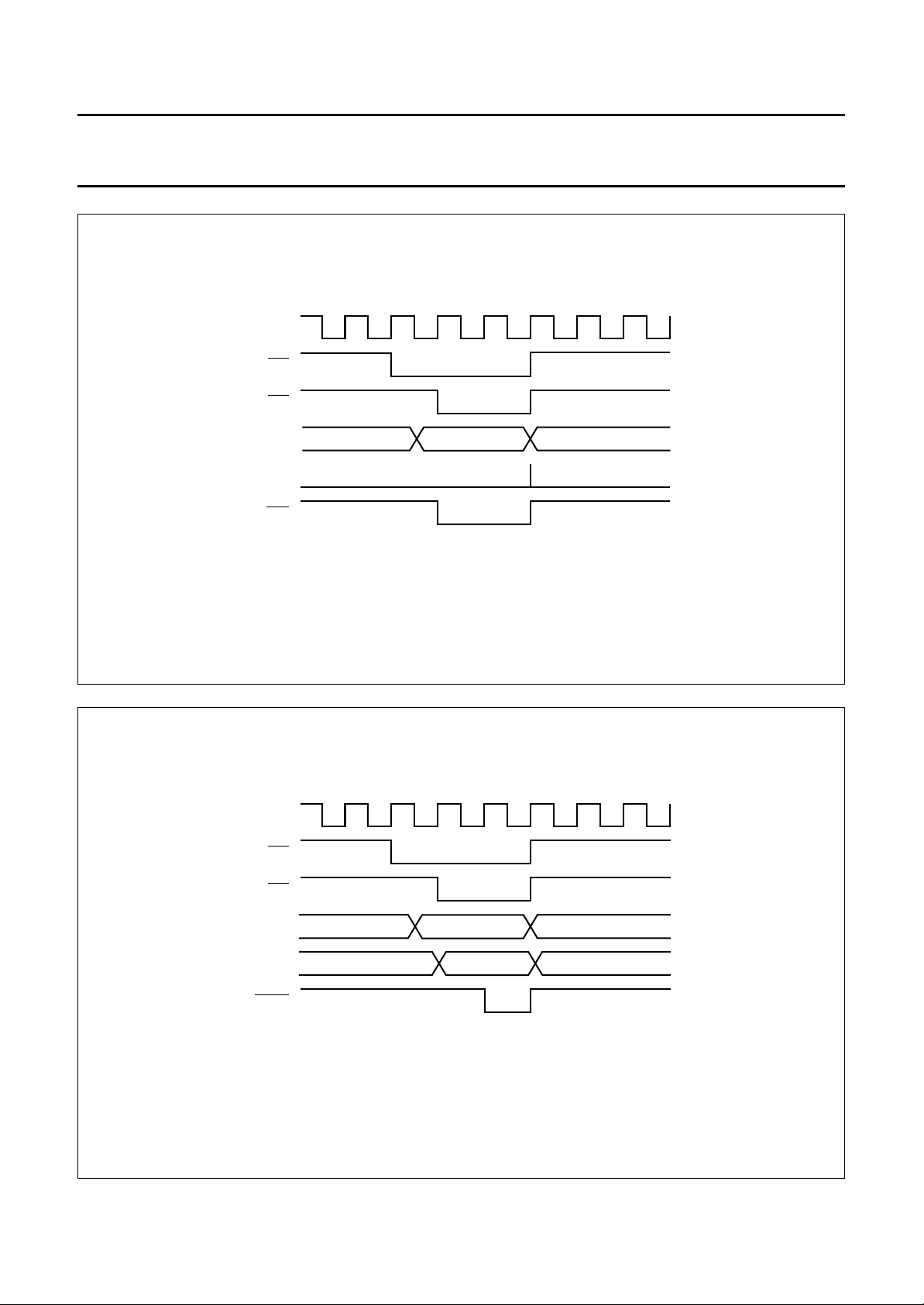
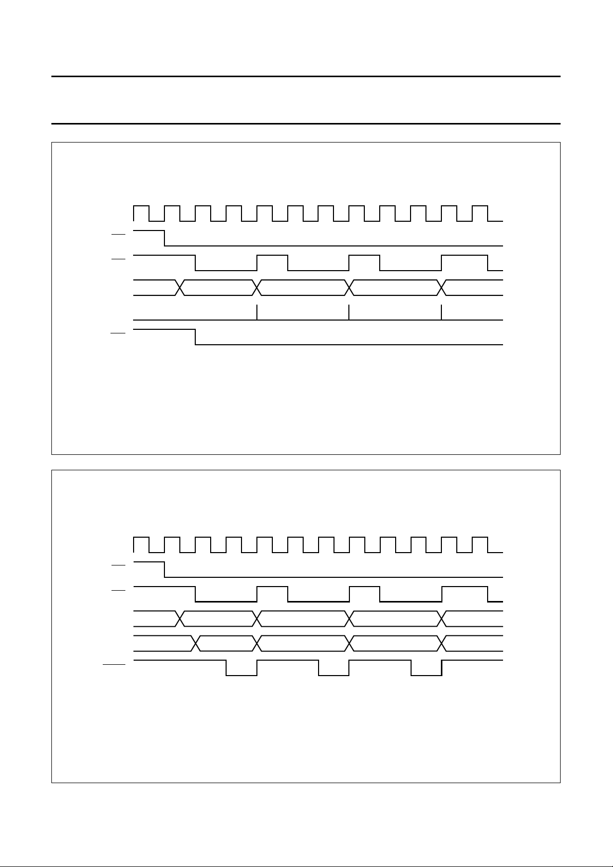
The required timing (see Figs 4 to 11) operate with the
industry standard 70 ns DRAMs. The interface is designed
to operate with one or two DRAMs using: 256 kbit × 4 or
1 Mbit × 4 devices. If a single DRAM is connected, all
access cycles require a page mode cycle to load both the
high and the low nibble of data. With a byte-wide memory
attached, a single byte cycle takes five clock cycles of
29.5 ns each, totalling 147.5 ns. In nibble mode, a single
byte cycle takes 236 ns.
UFFER MANAGER
1996 Jun 19 12

Philips Semiconductors Preliminary specification
Error correction and host interface IC for
CD-ROM (SEQUOIA)
handbook, full pagewidth
CLOCK
RAS
CAS
ADDRESS ROW COL COL
DATA
DOE
latch
low nibble
SAA7385
latch
high nibble
MGE390
handbook, full pagewidth
Fig.4 Nibble access read cycle.
CLOCK
RAS
CAS
ADDRESS ROW COL COL
DATA
WRITE
low-nibble high-nibble
MGE391
Fig.5 Nibble access write cycle.
1996 Jun 19 13
Philips Semiconductors Preliminary specification
Error correction and host interface IC for
CD-ROM (SEQUOIA)
handbook, full pagewidth
CLOCK
RAS
CAS
ADDRESS ROW COL
DATA
DOE
SAA7385
latch data
MGE392
handbook, full pagewidth
CLOCK
RAS
CAS
ADDRESS
DATA
WRITE
Fig.6 Byte mode single access read cycle.
ROW COL
DATA
MGE393
Fig.7 Byte mode single access write cycle.
1996 Jun 19 14

Philips Semiconductors Preliminary specification
Error correction and host interface IC for
CD-ROM (SEQUOIA)
handbook, full pagewidth
CLOCK
RAS
CAS
ADDRESS ROW COL1 COL2 COL3 COL4
DATA
DOE
latch latch latch
SAA7385
MGE394
handbook, full pagewidth
CLOCK
ADDRESS ROW COL1 COL2 COL3 COL4
DATA
WRITE
Fig.8 ECC burst access read cycle.
RAS
CAS
DATA1 DATA2 DATA3 DATA4
MGE395
Fig.9 ECC burst access write cycle.
1996 Jun 19 15
Philips Semiconductors Preliminary specification
Error correction and host interface IC for
CD-ROM (SEQUOIA)
handbook, full pagewidth
CLOCK
RAS
CAS
ADDRESS ROW COL1 COL2 COL3 COL4
DATA
DOE
latch data latch data latch data
SAA7385
MGE396
handbook, full pagewidth
CLOCK
RAS
CAS
ADDRESS ROW COL1 COL2 COL3 COL4
DATA
WRITE
Fig.10 SCSI standard burst access read cycle.
DATA1 DATA2 DATA3 DATA4
MGE397
Fig.11 SCSI standard burst access write cycle.
1996 Jun 19 16
Philips Semiconductors Preliminary specification
Error correction and host interface IC for
SAA7385
CD-ROM (SEQUOIA)
8 MICROCONTROLLER INTERFACE
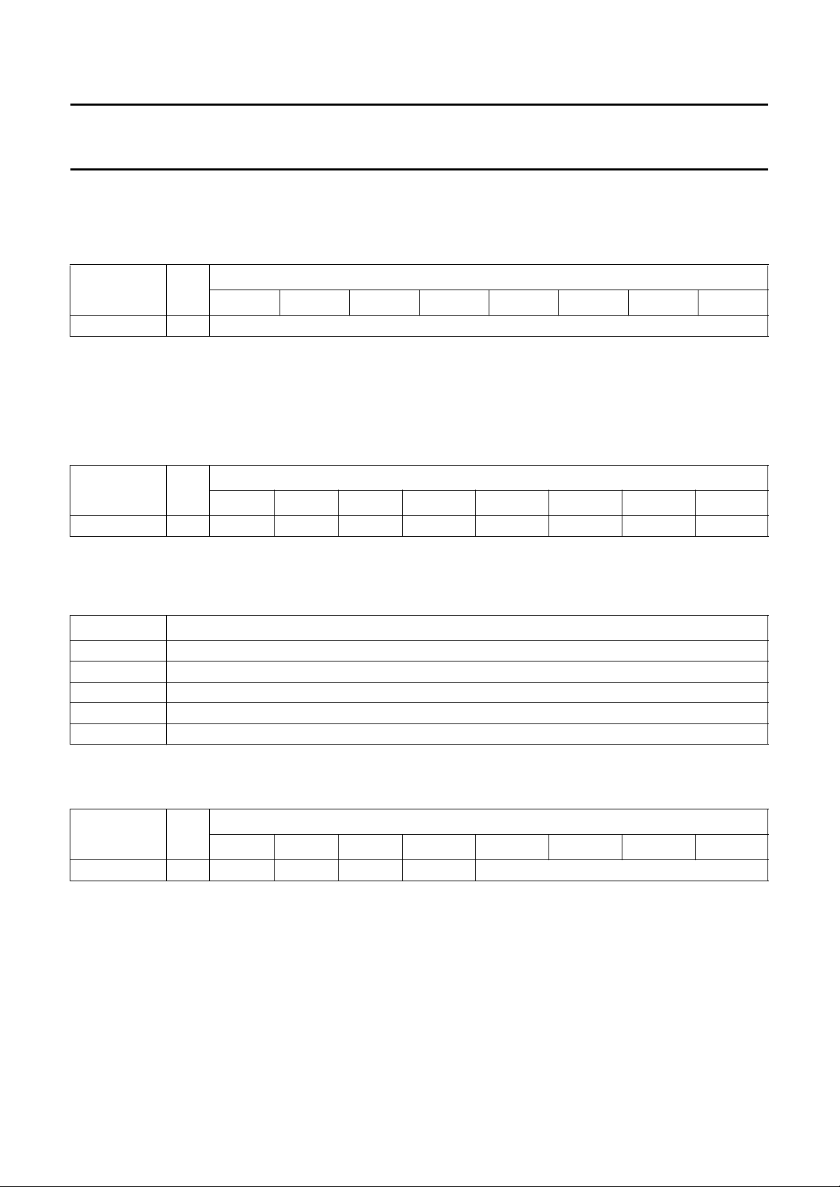
8.1 Microcontroller interface status register Table 1 NUM_COR register: 0xF08E
MNEMONIC R/W
76543210
NUM_COR R NUM_COR7 to NUM_COR0
Register 0xF08E indicates the number of corrections performed during the most recently executed
CORRECT_P_SYNDROMES or CORRECT_Q_SYNDROMES command. Note that NUM_COR is only valid after
completion of the CORRECT_P_SYNDROMES or CORRECT_Q_SYNDROMES command, and becomes invalid upon
execution of any other command.
Table 2 ECC_STATUS register: 0xF086
MNEMONIC R/W
76543210
ECC_STATUS R −−−FLG_EQ0 CRC_EQ0 PS_EQ0 QS_EQ0 ECC_ACT
DATA BYTE
DATA BYTE
Register 0xF086 provides status information on the current or last ECC command.
Table 3 ECC_STATUS definitions
MNEMONIC DESCRIPTION
ECC_ACT asserted while a command other than ASSERT_ABORT or RELEASE_ABORT remains active
QS_EQ0 asserted when all Q syndromes are zero
PS_EQ0 asserted when all P syndromes are zero
CRC_EQ0 asserted when the CRC remainder calculated by the CRC_CALCULATE command is all zeros
FLG_EQ0 asserted when all flag bytes in ECC RAM are zero
8.2 Microcontroller interface command register Table 4 ECCCTL register: 0xF085
MNEMONIC R/W
76543210
ECCCTL R/W −−− −ECC_COMMAND3 to ECC_COMMAND0
The ECC_COMMAND definitions are explained in Table 5.
DATA BYTE
1996 Jun 19 17

Philips Semiconductors Preliminary specification
Error correction and host interface IC for
CD-ROM (SEQUOIA)
Table 5 Definitions of ECC_COMMAND3 to ECC_COMMAND0
EEC_COMMAND DESCRIPTION
0000 ASSERT_ABORT
0001 RELEASE_ABORT
0010 CALCULATE_SYNDROMES (not Mode 2, Form 1)
0011 CALCULATE_SYNDROMES (Mode 2, Form 1)
0100 CRC_RECALCULATE (not Mode 2, Form 1)
0101 CRC_RECALCULATE (Mode 2, Form 1)
0110 COPY_RESULTS (not Mode 2, Form 1)
0111 COPY_RESULTS (Mode 2, Form 1)
1000 CORRECT_P_SYNDROMES
1001 CORRECT_Q_SYNDROMES
1100 TEST_ECC_ROM
1101 TEST_ECC_RAM_READ
1110 TEST_ECC_RAM_WRITE
Table 6 Command descriptions
SAA7385
COMMAND DESCRIPTION
ASSERT_ABORT Terminates any currently active operation and re-initializes the ECC logic. Remains in
reset state until occurrence of the RELEASE_ABORT command. At power-on reset,
the ECC is in the ASSERT_ABORT state. All microcontroller status bits are reset
when the ECC is in the ASSERT_ABORT state.
RELEASE_ABORT Terminates the ASSERT_ABORT command and enables activation of other
commands.
CRC_RECALCULATE Calculate CRC remainder buffer data, storing result in ECC RAM and updating
microcontroller status bit CRC_EQ0. Mode 2, Form 1 uses address 16 : 2075, or
0 : 2067; note 1.
CALCULA TE_SYNDROMES Prepares buffer for correction, calculates P and Q syndromes, and copies error flags
and CRC remainder from buffer to ECC RAM. The microcontroller status bits
PS_EQ0, QS_EQ0 and FLAGS_EQ0 are updated at the end of this operation.
1. Copy header from buffer to ECC RAM (Mode 2, Form 1 only)
2. Write to the buffer.
Not Mode 2, Form 1:
Address 0 → 0x00; Address1:10→0xFF; Address 11 → 0x00;
Address 2068 : 2075 → 0x00
Mode 2, Form 1:
Address 0 → 0x00; Add1:10→0xFF; Add 11 : 15 → 0x00
3. Read header and frame data from buffer to calculate P and Q syndromes
psyn[0 : 85].s1, psyn[0 : 85].s0, qsyn[0 : 51].s1 and qsyn[0 : 51].s0, storing
results in ECC RAM; see Table 76
4. Copy error flags from buffer to ECC RAM
5. Copy CRC remainder from buffer to ECC RAM
6. Update microcontroller status bits PS_EQ0, QS_EQ0 and FLAGS_EQ0.
1996 Jun 19 18

Philips Semiconductors Preliminary specification
Error correction and host interface IC for
SAA7385
CD-ROM (SEQUOIA)
COMMAND DESCRIPTION
COPY_RESULTS
CORRECT_P_SYNDROMES Scan all P syndromes and perform P-syndrome calculation. The microcontroller
CORRECT_Q_SYNDROMES Scan all Q syndromes and perform Q-syndrome calculation. The microcontroller
TEST_ECC_ROM Read each exponent and log in the alpha ROM to the NUM_COR register.
TEST_ECC_RAM_READ Read ECC RAM addresses 0 : 591 and copy to buffer addresses 0 : 591.
TEST_ECC_RAM_WRITE Read buffer addresses 0 : 591 and copy to ECC RAM addresses 0 : 591.
Copies current ECC RAM contents to the buffer memory:
1. Copy header flags from ECC RAM to buffer (Mode 2, Form 1 only)
2. Copy error Flags from ECC RAM to buffer
3. Copy CRC remainder from ECC RAM to buffer
4. Copy P syndromes from ECC RAM to buffer
5. Copy Q syndromes from ECC RAM to buffer.
status bits PS_EQ0, QS_EQ0 and FLAGS_EQ0 are updated at the end of this
operation.
status bits PS_EQ0, QS_EQ0 and FLAGS_EQ0 are updated at the end of this
operation.
This command may only be terminated by the ASSERT_ABORT command.
Note
1. 16 : 2075 and 0 : 2067 are address frame offsets. The frame buffer organization is shown in Table 75.
8.3 Microcontroller interrupts
An interrupt pulse is generated upon completion of any of the following commands:
• CALCULATE_SYNDROMES (not Mode 2, Form 1)
• CALCULATE_SYNDROMES (Mode 2, Form 1)
• CRC_RECALCULATE (not Mode 2, Form 1)
• CRC_RECALCULATE (Mode 2, Form 1)
• COPY_RESULTS (not Mode 2, Form 1)
• COPY_RESULTS (Mode 2, Form 1)
• CORRECT_P_SYNDROMES
• CORRECT_Q_SYNDROMES
• TEST_ECC_ROM
• TEST_ECC_RAM_READ
• TEST_ECC_RAM_WRITE.
If a command is aborted by the ASSERT_ABORT command, a spurious interrupt may be generated within five clock
cycles of the ASSERT_ABORT command.
1996 Jun 19 19

Philips Semiconductors Preliminary specification
Error correction and host interface IC for
SAA7385
CD-ROM (SEQUOIA)
Table 7 Command execution times
COMMAND CYCLES
CALCULATE_SYNDROMES (not Mode 2, Form 1) 5604 186.8 2658
CALCULATE_SYNDROMES (Mode 2, Form 1) 5600 186.7 2654
CRC_RECALCULATE (not Mode 2, Form 1) 4136 137.9 2068
CRC_RECALCULATE (Mode 2, Form 1) 4120 137.3 2060
COPY_RESULTS (not Mode 2, Form 1) 1148 38.3 574
COPY_RESULTS (Mode 2, Form 1) 1156 38.5 578
CORRECT_P_SYNDROMES
(maximum addition per correction)
CORRECT_Q_SYNDROMES
(maximum addition per correction)
TEST_ECC_RAM_READ 1184 39.5 592
TEST_ECC_RAM_WRITE 1184 39.5 592
All times indicated reflect two clock cycles per memory access for all accesses other than P and Q corrections. P and Q
corrections reflect seven clock cycles per memory access. Execution times will be extended due to refresh timing, other
buffer traffic, and configuration of nibble-wide memory.
1466
157
888
167
TIME (µs)
at 33 MHz
48.9
5.2
29.6
5.6
MEMORY
ACCESSES
0
2
0
2
8.3.1 I
Two registers are used to control the operation of the interrupt logic. The register INTRMSK allows each interrupt to be
enabled or disabled. INTRMSK and INTRFLG are cleared on reset to initially disable and clear all interrupts; the output
latch controlling the INT line is set on a reset; this must be cleared by writing 0x00 to INTRFLG. To enable an interrupt,
the bit that corresponds to the interrupt in INTRFLG must be set. The INTRFLG register shows the status of the
interrupts. If any bit is HIGH then an interrupt has occurred since the last time the bit was cleared. Writing a zero to any
bit location in INTRFLG will clear the corresponding interrupt. If a masked interrupt occurs, the microcontroller can still
detect the occurrence because the event is still posted in INTRFLG.
Table 8 Interrupt mask register: 0xF0FB
MNEMONIC R/W
INTRMSK R/W MASK7 MASK6 MASK5 MASK4 MASK3 MASK2 MASK1 MASK0
Each bit in register 0xF0FB corresponds to the interrupt at the same bit location in register 0xF0FC. To enable an
interrupt, the bit in this register must be set HIGH.
Table 9 Interrupt flag register: 0xF0FC
MNEMONIC R/W
NTERRUPT REGISTER DEFINITIONS
DATA BYTE
76543210
DATA BYTE
765 4 3210
INTRFLG R/W − FETXINT FERXINT ECC_COR FE_HDR FE2352 STR_LST FRM_STR
If any bit is set in this register (Table 9) then an interrupt may be sent to the microcontroller. Table 10 shows when the
interrupts are asserted; assuming the corresponding mask bit is set.
1996 Jun 19 20
 Loading...