

Philips SAA7384GP, SAA7384ZP Datasheet

DATA SH EET
Preliminary specification
File under Integrated Circuits, IC02
1996 Oct 24
INTEGRATED CIRCUITS
SAA7284
Terrestrial digital sound decoder for
conventional intercarrier PLL-IF
systems

1996 Oct 24 2
Philips Semiconductors Preliminary specification
Terrestrial digital sound decoder for
conventional intercarrier PLL-IF systems
SAA7284
FEATURES
• Single-chip solution including FM and vision filters,
analog demodulator and audio switching
• Dual standard with automatic selection between PAL
system I and BGH
• Suitable for conventional intercarrier PLL-IF
(single SAW) TV/VCR systems
• Single low-radiation crystal oscillator for improved EMC
• Stereo bitstream audio DACs
• Programmable attenuator for matching levels of NICAM
and FM audio sources at the output of the device
• Full EBU specification NICAM 728 demodulation and
decoding
• Digital Audio Interface conforming with EBU/IEC 958
• Automatic mute function which switches from NICAM to
FM sound when NICAM fails
• Compatible with either single-ended or differential
DQPSK input signals
• Microcomputer controlled via I2C-bus (up to 400 kHz
specification).
APPLICATIONS
• Television receivers
• Video cassette recorders.
GENERAL DESCRIPTION
Philips Semiconductors have pushed the boundaries of
Stereo Sound further with this addition to the successful
Terrestrial Digital Sound Decoder family. The SAA7284
device is an application specific version of the existing
SAA7283, with guaranteed improved specification on
selected parameters, enabling comparable RF
performance in conventional intercarrier PLL-IF systems,
to that of the SAA7283 in QSS systems.
The SAA7284 takes, as input, a second IF (intercarrier)
Terrestrial TV PAL signal, and performs all the Differential
Quadrature Phase Shift Keying (DQPSK) demodulation,
digital decoding and digital-to-analog conversion
necessary to produce a complete NICAM receiver on a
single integrated circuit.
The demodulator function includes integrated baseband
filters for pulse shaping and unwanted signal rejection,
automatic gain control, a low jitter integrated VCO, digital
monostables for precise data sampling points and a
multi-standard controller to enable automatic locking to
either a PAL system I or PAL system BGH input signal.
The decoder function performs the descrambling,
de-interleaving and reformatting operations required to
recover the original data words.
The data words are processed through a stereo digital
filter, digital de-emphasis network, second order noise
shaper and 256 times oversampling Bitstream audio DAC.
ORDERING INFORMATION
TYPE
NUMBER
PACKAGE
NAME DESCRIPTION VERSION
SAA7284ZP SDIP52 plastic shrink dual in-line package; 52 leads (600 mil) SOT247-1
SAA7284GP QFP64 plastic quad flat package; 64 leads (lead length 1.95 mm);
body 14 × 20 × 2.8 mm
SOT319-2

1996 Oct 24 3
Philips Semiconductors Preliminary specification
Terrestrial digital sound decoder for
conventional intercarrier PLL-IF systems
SAA7284
QUICK REFERENCE DATA
SYMBOL PARAMETER MIN. TYP. MAX. UNIT
V
DD
supply voltage 4.5 5.0 5.5 V
I
DD
supply current − 205 − mA
f
clk
clock frequency − 8.192 − MHz
T
amb
operating ambient temperature −20 +25 +70 °C
1996 Oct 24 4
Philips Semiconductors Preliminary specification
Terrestrial digital sound decoder for
conventional intercarrier PLL-IF systems
SAA7284
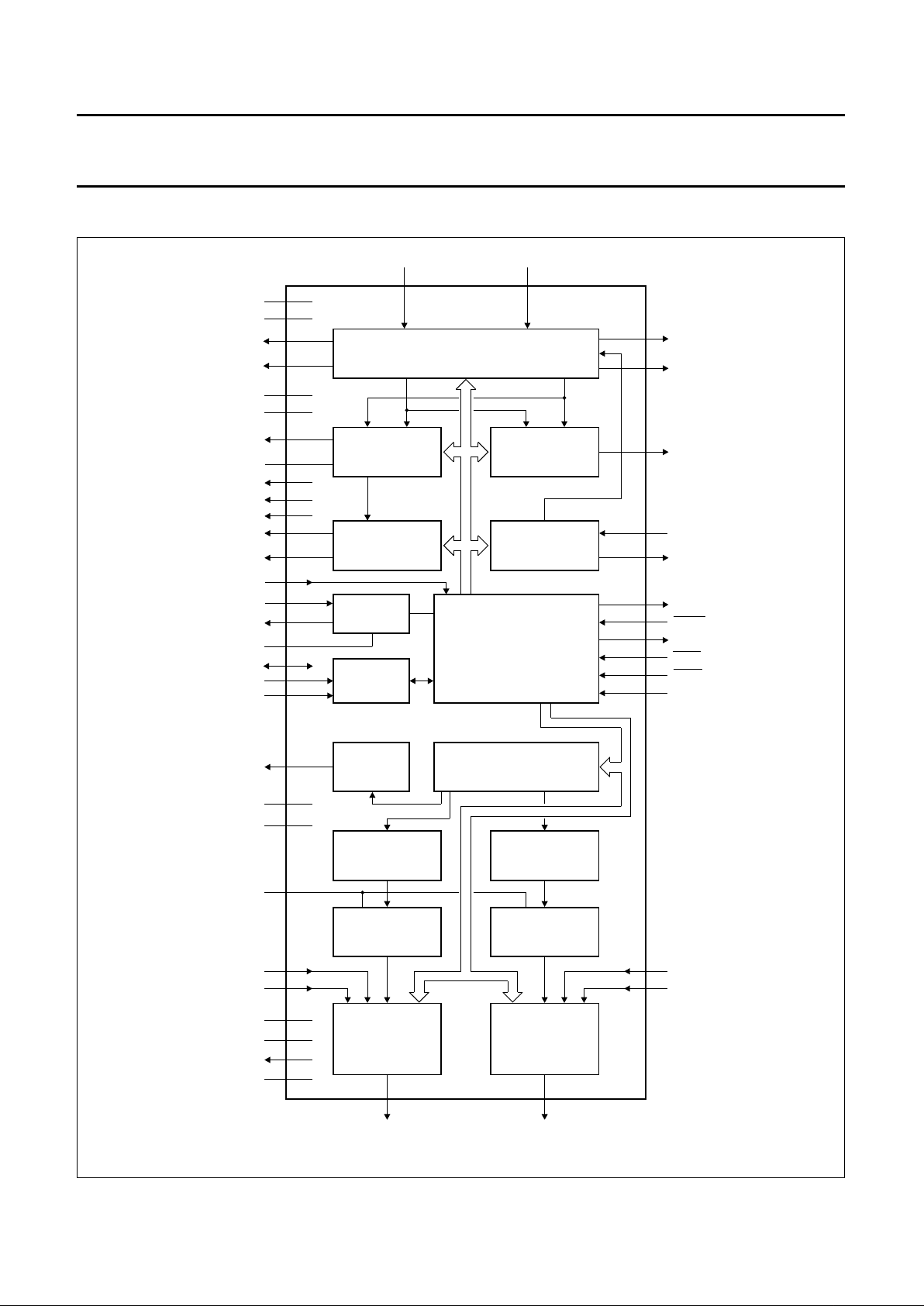
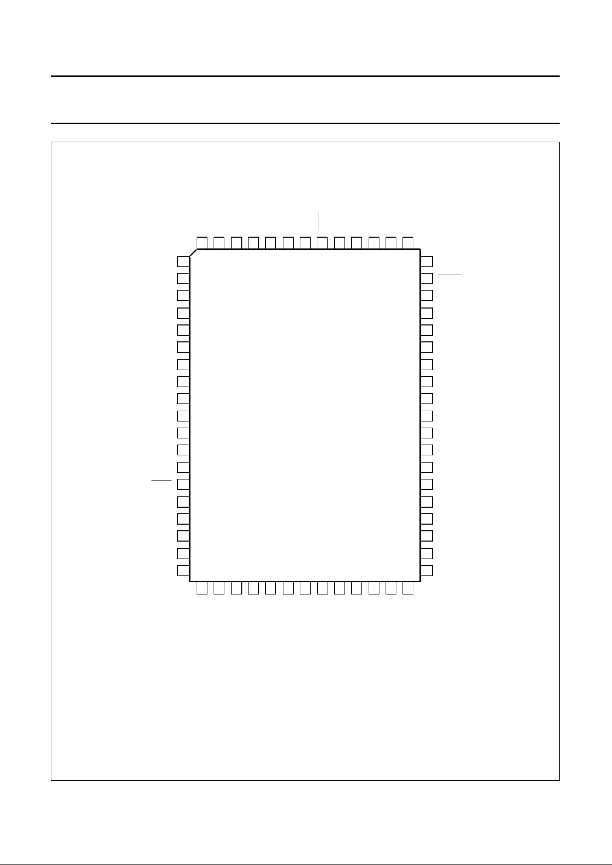
BLOCK DIAGRAM
handbook, full pagewidth
QUADRATURE MIXERS, BASEBAND FILTERS
AND
AGC GAIN STAGE
MBH216
PORT2
ADSEL
DOBM
SDA
SCL
DATAOUT
EXTR
FMR
PCLK
OPR
DATAIN
OSC
XTAL
CLKLPF
OPL
FML
EXTL
PORM
PORA
REMVE
PKDET
REMO
CEYE
SEYE
COFF
SOFF
DQPSK MIXREF
VCLK
VCONT
V
DDD
V
SSD
V
SSX
V
SSF2
V
DDF2
V
RCF
I
REF
V
ROF
V
DDF1
V
SSF1
V
SSDAC
V
ROA
V
RCA
V
SSA
V
DDA
MUTE
RESET
SAA7284GP
COSINE
SINE
CARRIER LOOP
PHASE DETECTOR
AND DATA SLICERS
AGC
CONTROLLER
BITRATE
CLOCK
RECOVERY
CARRIER LOOP
QUADRATURE
VCO
CRYSTAL
OSCILLATOR
I C
2
DAI
DIGITAL FILTER, GAIN,
J17 DE-EMPHASIS
NOISE SHAPER
(RIGHT CHANNEL)
BITSTREAM DAC
(RIGHT CHANNEL)
OUTPUT
SWITCHES
AND
BUFFER
(RIGHT CHANNEL)
NOISE SHAPER
(LEFT CHANNEL)
BITSTREAM DAC
(LEFT CHANNEL)
OUTPUT
SWITCHES
AND
BUFFER
(LEFT CHANNEL)
NICAM 728 DECODER
AND
DEVICE CONTROLLER
11 4
(1)
54
53
55
43
42
44
46
41
45
59
49
48
8
12
13
61
62
7
63
34
21
22
27
24
47
50
56
57
14
15
3
2
38
39
30
31
25
23
16
17
36
35
37
29 28
Fig.1 Block diagram (QFP64).
(1) Represents controller bus.
1996 Oct 24 5
Philips Semiconductors Preliminary specification
Terrestrial digital sound decoder for
conventional intercarrier PLL-IF systems
SAA7284
PINNING
SYMBOL
PIN
DESCRIPTION
SDIP52 QFP64
(1)
MUTE 1 57 active LOW mute input; function defined by MUTEDEF (control bit in the
I2C-bus register)
DOBM 2 59 digital audio interface output that can be 3-stated via I
2
C-bus
V
DDA
3 61 analog supply voltage for the audio channels
V
SSA
4 62 analog ground connection for the audio channels
V
RCA
5 63 internal audio reference voltage buffer (high-impedance node)
EXTR 6 2 external analog input to the right audio channel
FMR 7 3 FM sound input to the right audio channel
OPR 8 4 analog output from the right audio channel
n.c. 9 and 10 9 and 10 not connected; left open-circuit in application
V
ROA
11 7 internal audio reference voltage buffer output
V
SSDAC
12 8 quiet ground connection to DACs
n.c. 13 and 14 − not connected; left open-circuit in application
OPL 15 11 analog output from the left audio channel
FML 16 12 FM sound input to the left audio channel
EXTL 17 13 external analog input to the left audio channel
PORM 18 14 active LOW power-on reset mute input; mute cleared by setting silence bit
HIGH in I2C-bus (internal pull-up)
PORA 19 15 power-on reset audio select input (internal pull-up)
REMVE 20 16 carrier loop-filter connection
REMO 21 17 carrier loop-filter output
SEYE 22 21 sine channel eye pattern output for monitoring
SOFF 23 22 sine channel offset compensator capacitor output
V
SSF1
24 23 demodulator ground connection 1
VCLK 25 24 carrier loop VCO clock output for monitoring
V
DDF1
26 25 demodulator supply voltage 1
VCONT 27 27 carrier loop VCO control voltage input
MIXREF 28 28 mixer voltage reference or input when using differential DQPSK signal
DQPSK 29 29 DQPSK input signal
COFF 30 30 cosine channel offset compensator capacitor output
CEYE 31 31 cosine channel eye pattern output for monitoring
PKDET 32 34 AGC peak detector storage capacitor output
V
ROF
33 35 internal demodulator reference voltage buffered output
I
REF
34 36 internal demodulator reference current output
V
RCF
35 37 internal demodulator reference voltage unbuffered output
V
DDF2
36 38 demodulator supply voltage 2
V
SSF2
37 39 demodulator ground connection 2
n.c. 38 40 not connected; left open-circuit in application
CLKLPF 39 41 clock loop-phase comparator output
1996 Oct 24 6
Philips Semiconductors Preliminary specification
Terrestrial digital sound decoder for
conventional intercarrier PLL-IF systems
SAA7284
Note
1. Pins 1, 5, 6, 18, 19, 20, 26, 32, 33, 51, 52, 58, 60 and 64 are not connected; left open-circuit in application.
XTAL 40 42 8.192 MHz crystal oscillator input
OSC 41 43 8.192 MHz crystal oscillator output
V
SSX
42 44 crystal oscillator ground connection
DATAIN 43 45 serial data input at 728 kbits/s to decoder
V
SSD
44 48 digital ground connection
PCLK 45 47 728 kHz output clock to DQPSK demodulator
V
DDD
46 49 digital supply voltage
RESET 47 50 active LOW power-on reset input
DATAOUT 48 46 serial data output at 728 kbits/s from DQPSK demodulator
SCL 49 53 serial clock input for I
2
C-bus
SDA 50 54 serial data input/output for I
2
C-bus
ADSEL 51 55 input that defines I
2
C-bus address bit 0 (internal pull-up)
PORT2 52 56 output that is directly controlled from Port 2 bit in I
2
C-bus
SYMBOL
PIN
DESCRIPTION
SDIP52 QFP64
(1)
1996 Oct 24 7
Philips Semiconductors Preliminary specification
Terrestrial digital sound decoder for
conventional intercarrier PLL-IF systems
SAA7284
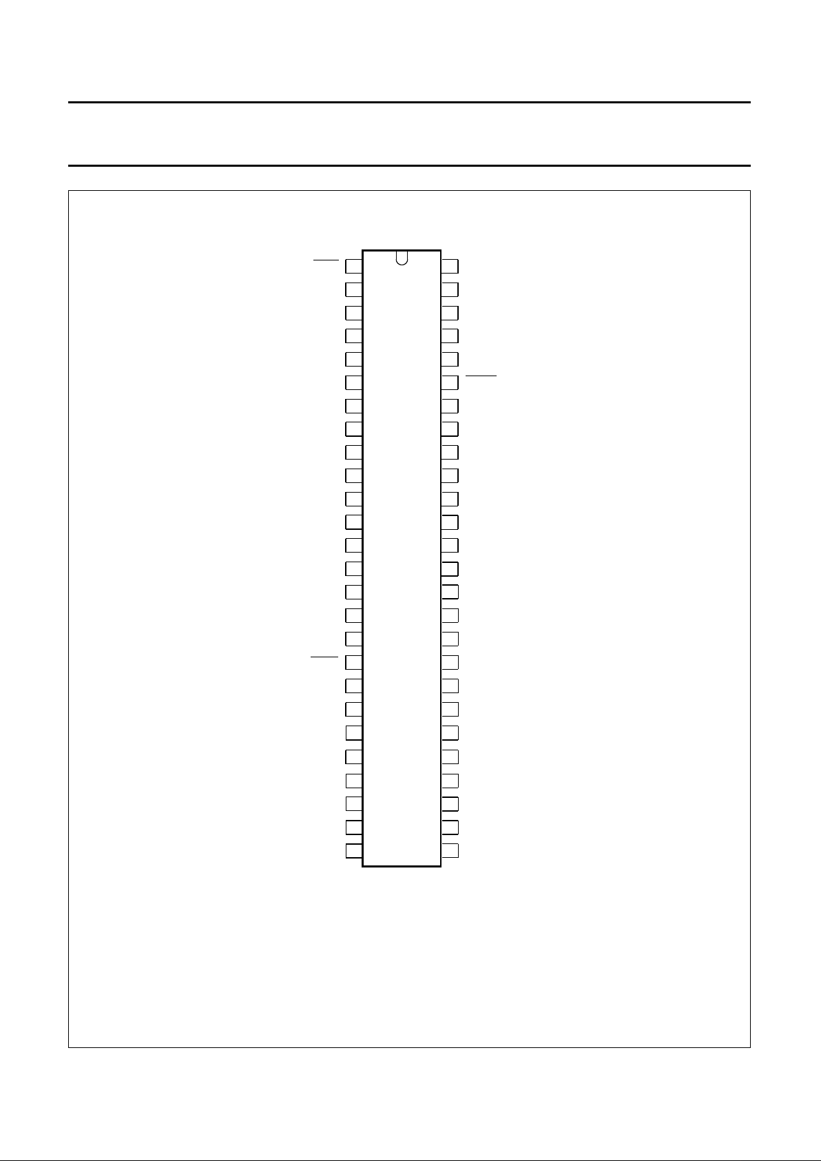
Fig.2 Pin configuration for SOT247.
handbook, halfpage
1
2
3
4
5
6
7
8
9
10
11
12
13 40
39
38
37
36
35
34
33
32
31
30
29
28
27
14
15
16
17
18
19
20
22
23
24
25
26
21
42
41
43
44
45
46
47
48
49
50
51
52
MBH217
PORT2
ADSELDOBM
SDA
SCL
DATAOUT
EXTR
FMR
PCLK
OPR
n.c.
DATAIN
n.c.
OSC
XTAL
n.c.
CLKLPF
n.c.
OPL
FML
EXTL
PORM
PORA
REMVE
PKDETREMO
CEYESEYE
COFFSOFF
DQPSK
MIXREFVCLK
VCONT
V
DDD
V
SSD
V
SSX
V
SSF2
V
DDF2
V
RCF
I
REF
V
ROF
V
DDF1
V
SSF1
V
SSDAC
V
ROA
V
RCA
V
SSA
V
DDA
MUTE
RESET
n.c.
SAA7284ZP
1996 Oct 24 8
Philips Semiconductors Preliminary specification
Terrestrial digital sound decoder for
conventional intercarrier PLL-IF systems
SAA7284
Fig.3 Pin configuration for SOT319.
handbook, full pagewidth
1
2
3
4
5
6
7
8
9
10
11
12
13
14
15
16
17
18
19
51
50
49
47
46
45
44
43
42
41
40
39
38
37
36
35
34
33
48
20
21
22
24
25
26
27
28
29
30
31
32
23
64
63
62
60
59
58
57
56
55
54
53
52
61
MBH218
DATAOUT
EXTR
FMR
PCLK
OPR
n.c.
DATAIN
n.c.
OSC
XTAL
n.c.
CLKLPF
n.c.
OPL
FML
EXTL
PORM
PORA
REMVE
PKDET
REMO
V
DDD
V
SSD
V
SSX
V
SSF2
V
DDF2
V
RCF
I
REF
V
ROF
V
SSDAC
V
ROA
RESET
n.c.
SAA7284GP
n.c.
n.c.
n.c.
n.c.
n.c.
CEYE
SEYE
COFF
SOFF
DQPSK
MIXREF
VCLK
VCONT
V
DDF1
V
SSF1
n.c.
n.c.
n.c.
PORT2
ADSEL
DOBM
SDA
SCL
V
RCA
V
SSA
V
DDA
MUTE
n.c.
n.c.
n.c.
n.c.

1996 Oct 24 9
Philips Semiconductors Preliminary specification
Terrestrial digital sound decoder for
conventional intercarrier PLL-IF systems
SAA7284
FUNCTIONAL DESCRIPTION
DQPSK demodulation
Q
UADRATURE MIXERS, BASEBAND FILTERS AND AUTOMATIC
GAIN CONTROL
(AGC)
The DQPSK signal is fed into two differential input mixers,
where it is mixed with quadrature phases generated by the
carrier-loop quadrature VCO. The quadrature signals
modulated onto the NICAM carrier are thus recovered.
The mixers can be driven by either a single-ended or
differential source. In single-ended mode, the device is
driven directly from the sound IF down-converter into the
DQPSK input pin, with the MIXREF pin decoupled.
In differential mode, the signal is applied between the
DQPSK and MIXREF pins.
The outputs from the mixers are then fed into a
pulse-shaping filter, and FM/vision filter stage with
improved colour rejection to allow suitable performance
with SAW filters. The signal from the filtering stages is then
fed into the AGC, which ensures that the phase
comparator gain remains constant, irrespective of the
input signal level. This is important to maintain the stability
of Costas loop PLL.
AGC
CONTROLLER
The AGC controller monitors the I and Q channel signals
at the input to the carrier loop-phase comparator and
generates a reference voltage to set the AGC output level.
E
YE BUFFER
A differential to the single-ended converter provides the
baseband signal as an output at the pins CEYE and SEYE
for the I and Q channels respectively for eye-height
monitoring.
B
IT RATE CLOCK RECOVERY
The I and Q channels are processed using edge detectors
and monostables, which generate a signal with a coherent
component at the data symbol rate. The outputs from the
I and Q channel monostables are each compared with the
clock derived from PCLK (364 kHz nominal), the resultant
output is used to derive a 3-state control signal used to
control two current sources at the CLKLPF output.
This error signal is loop filtered and used to control the
master clock oscillator. The bit rate clock, PCLK, and
symbol clock are derived from the master clock.
NICAM 728 decoding
D
ECODING FUNCTIONS
The device performs all decoding functions in accordance
with the EBU NICAM 728 specification. After locking to the
frame alignment word, the data is de-scrambled by
application of the defined pseudo random binary
sequence, and the device synchronizes to the periodic
frame flag bit C0.
The relevant control information and scale factor word is
extracted, and with the integrated RAM the data is
de-interleaved and the scale factor word is extracted, and
expanded to 14 bits. Parity checking on the eleventh bit of
each sample word is carried out to reveal any sound
sample errors, which if detected are flagged, with the last
good sample being held.
Automatic muting
Enable when AMDIS = LOW. The I
2
C-bus section has two
registers which define an upper and lower limit for the
automatic muting function. When the number of errors
within a 128 ms period exceeds the number stored in the
upper error limit register, then the automatic muting will
switch the device output to the FM input, (dependent on
the relevant control bits in the I2C-bus) and mute (set to
zero) the data input to the filter (in that order). When the
error count in a 128 ms period is less than the value stored
in the lower error limit register then the data into the filter
is uninterrupted, and the device output is switched back to
the DAC (dependent on the value of the relevant control
bits in the I2C-bus). During the muting operation the
open-drain pin MUTE is pulled LOW and the AM bit in the
status-byte is set HIGH. Figure 4 shows the dependency
of the automatic muting function on error_count, RSSF,
C4OV, output state and application mode. The automatic
muting function, if enabled, will override user mute via the
MUTE pin/bit.
When the transmission is DATA format or currently
undefined format (C3 = logic 1) the device will
automatically switch to the FM inputs regardless of
RSSF/C4OV states, and whether the automatic muting
function AMDIS is enabled or disabled.

1996 Oct 24 10
Philips Semiconductors Preliminary specification
Terrestrial digital sound decoder for
conventional intercarrier PLL-IF systems
SAA7284
User mute
The error counter is an 8-bit counter which locks at
count 255. The counter is reset and its output sent to the
I2C-bus every 128 ms. This enables the user to interrogate
the number of errors occurring within a 128 ms period.
The user can then mute the device by pulling pin MUTE
LOW (this function is also provided by the MUTE bit in the
I2C-bus) or setting SILENCE bit LOW in I2C-bus to switch
input of audio switching buffers to analog ground.
Switching buffers
The analog switches select between the output of the
DACs, the FM input and an external input (EXT).
Switching is controlled by bits in the I
2
C-bus and internal
switching function. The external analog inputs should be
≤1.1 V (RMS) at the input pin, and the output buffers have
a voltage drive of 1 V (RMS).
NICAM/FM audio level matching
Differing audio headroom and alignment levels occur
between systems I and BGH, due to the differing systems
and broadcast standards. In order to match the NICAM
and FM audio output levels without requiring application
changes, the device will automatically switch in 4.6 dB
attenuation network in the NICAM path for system BGH
(this can be disabled by setting the NICLEV bit LOW in
I
2
C-bus). A programmable attenuation network in the FM
path only, controlled by bits in I2C-bus, provides additional
flexibility for user to match FM and NICAM audio levels
(see Table 9).
Power-on reset state
Two pins control the initial set-up of the device during
power-on reset.
PORA (Power-On Reset Audio)
When pulled LOW the device will be configured with a
12 dB gain in the oversampling filter and theC4OV bit in
the I2C-bus will be set HIGH. This pin when HIGH will
configure the device with a 6 dB gain in the
oversampling filter and will set C4OV bit in the I2C-bus
LOW.
PORM (Power-On Reset Mute)
This pin when LOW will mute the output of the device at
power-on by setting the SILENCE bit in the I2C-bus
LOW. To put the device back into a normal mode of
operation the SILENCE bit in the I2C-bus must be set
HIGH.

1996 Oct 24 11
Philips Semiconductors Preliminary specification
Terrestrial digital sound decoder for
conventional intercarrier PLL-IF systems
SAA7284
Fig.4 Flow diagram showing SAA7284 automatic muting function.
(1) Indicating that a mute may occur when user returns to NICAM source.
handbook, full pagewidth
MGB465
DUAL MONO MODE
LEFT = RIGHT = M1
SELECTED
SOUND APPLICATION
DUAL MONO
ERROR_COUNT
ERROR_MAX
EXT or FM INPUT
SWITCHED IN
C4ov BIT = 0
Output is
unchanged
AM bit = LOW
MUTEB pin = HIGH
Output is
unchanged
AM bit = HIGH
MUTEB pin = LOW
(1)
(1)
RSSF = 1
Output is switched
to FM input
AM bit = HIGH
MUTEB pin = LOW
Output is
unchanged
AM bit = LOW
MUTEB pin = HIGH
Output is
unchanged
AM bit = LOW
MUTEB pin = HIGH
NO
NO
NO
NO
YES
YES
YESYES
YES
NO
NO
YES
When error_count is less
than error_min, the output
is switched back to NICAM
and AM bit = LOW,
MUTEB pin = HIGH
When error_count is
less than error_min,
AM bit = LOW,
MUTEB pin = HIGH
1996 Oct 24 12
Philips Semiconductors Preliminary specification
Terrestrial digital sound decoder for
conventional intercarrier PLL-IF systems
SAA7284
I2C-BUS FORMATS
The SAA7284 contains an I2C-bus slave transceiver (up to 400 kHz) permitting a master device to:
• Read decoder status information derived from the transmitted digital audio signal
• Read an error count byte to determine the bit error rate for user mute purposes and to indicate quality of NICAM signal
• Write control codes to select PAL I or PAL BGH configurations
• Write control codes to select the available analog switching configurations
• Write upper and lower error count limits for automatic muting function
• Read additional transmitted data bits. Their purpose has yet to be defined but accessibility is provided to allow future
services to be implemented in receiver software.
I
2
C-bus slave address
An address select pin (ADSEL) is provided to allow selection of one of two different slave addresses. The logic state of
the ADSEL pin is reflected in the least significant bit of the I2C-bus slave address.
Slave address = 101101X (R/W) [ADSEL = 1, address = B6 (R/W) ADSEL = 0, address = B4 (R/W)].
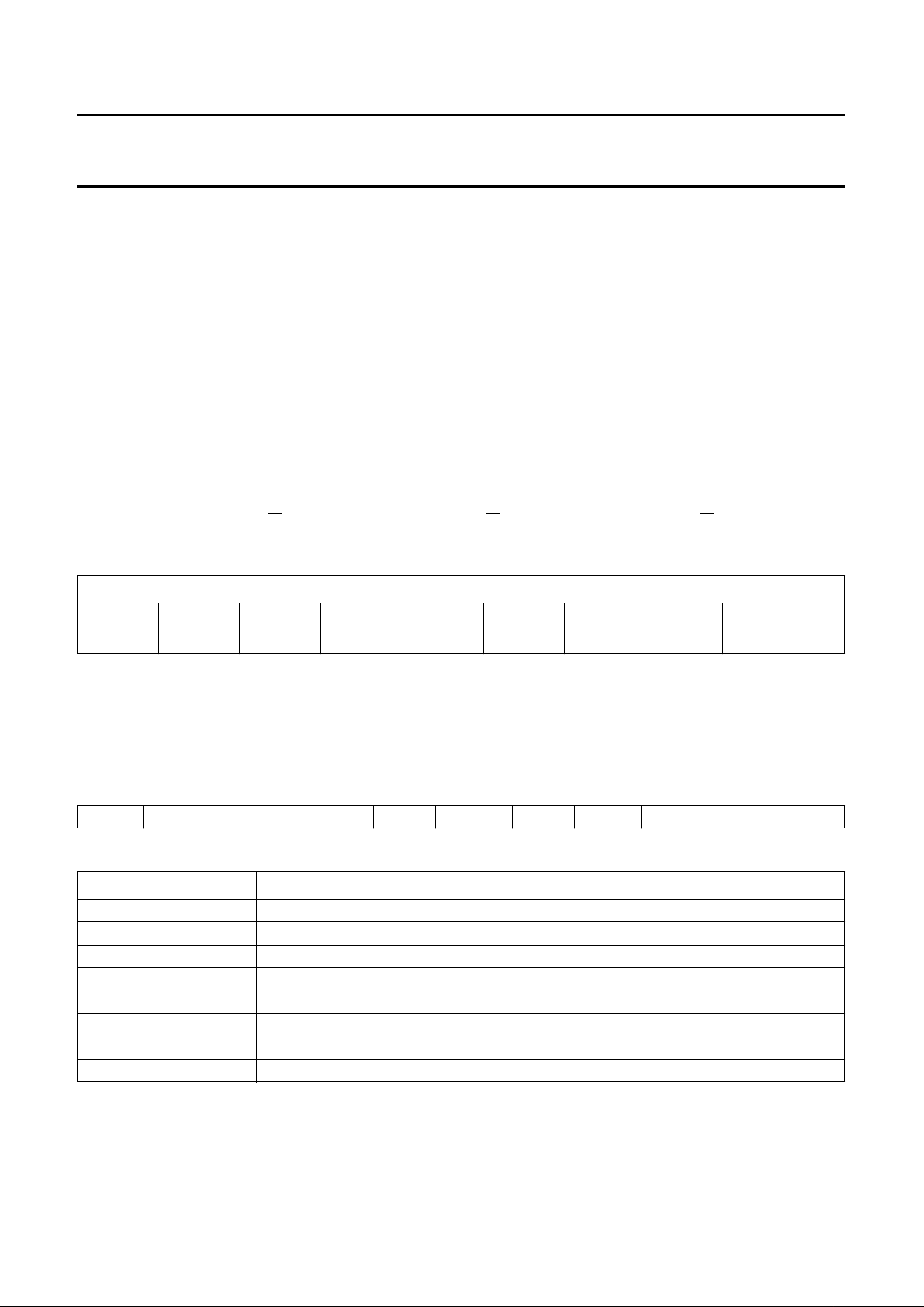
Table 1 SAA7284 slave address
The SAA7284 does not acknowledge the I2C-bus general call address.
Slave receiver format
The slave receiver format is shown in Table 2.
Table 2 Slave receiver format
Table 3 Explanation of Table 2
The sub-address is auto-incremented by the SAA7284, for each data byte received. When the sub-address is equal to
04 (HEX), on reception of the next data byte, the sub-address will reset to 00 (HEX).
BITS
A7 A6 A5 A4 A3 A2 A1 A0
1 0 1 1 0 1 selected by ADSEL read/write
START slave_addr ACK sub_addr ACK data_byte ACK n-bytes data_byte ACK STOP
ITEM DESCRIPTION
START I
2
C-bus start condition
Slave_addr 101101XW
X logic 0 when ADSEL = 0; logic 1 when ADSEL = 1
W logic 0, I
2
C-bus write to slave receiver
ACK I
2
C-bus acknowledge condition generated by slave receiver
Sub_addr sub-address range 00 to 04 (HEX)
Data_byte data byte transmitted to slave receiver
STOP I
2
C-bus stop condition
 Loading...