

Philips SAA7380GP Datasheet

INTEGRATED CIRCUITS
DATA SH EET
SAA7380
Error correction and host interface
IC for CD-ROM (ELM)
Preliminary specification
File under Integrated Circuits, IC01
1996 Apr 25

Philips Semiconductors Preliminary specification
Error correction and host interface IC for
CD-ROM (ELM)
CONTENTS
1 FEATURES
2 GENERAL DESCRIPTION
3 QUICK REFERENCE DATA
4 ORDERING INFORMATION
5 BLOCK DIAGRAM
6 PINNING
7 FUNCTIONAL DESCRIPTION
7.1 CD-DSP interface and data input
7.2 Error correction and EDC check
7.3 Host interface
7.4 Subcode channel Q-to-W buffering
7.5 External buffer memory
7.6 Sub-CPU registers
7.7 Register Descriptions
7.8 Sub-CPU interface
7.9 Host registers
.10 CD-DSP Timings
8 LIMITING VALUES
9 THERMAL CHARACTERISTICS
10 CHARACTERISTICS
11 TIMING CHARACTERISTICS
11.1 Q-to-W subcode interface timing
11.2 External memory SRAM timing
11.3 External memory DRAM timing
11.4 Sub-CPU interface timing
11.5 ATAPI host interface timing
11.6 SANYO compatibility mode host interface
timing
11.7 Oak compatibility mode host interface timing
11.8 Crystal oscillator
12 PACKAGE OUTLINE
13 SOLDERING
14 DEFINITIONS
15 LIFE SUPPORT APPLICATIONS
SAA7380
1996 Apr 25 2

Philips Semiconductors Preliminary specification
Error correction and host interface IC for
CD-ROM (ELM)
1 FEATURES
• CD-ROM (Mode 1) and CD-I (Mode 2 - Form 1 and
Form 2) formats supported
• Real-time error detection and correction in hardware
• Suitable for 6 × speed, n = 6
• Maximum host transfer burst rate of 11.1 Mbyte/s
• Corrects two errors per symbol with erasure correction
• 36 kbit of on-chip error correction buffer RAM
• 12-byte command FIFO and 12-byte status FIFO
• Compatible with the Advanced Technology Attachment
(ATA) register set and the Advanced Technology
Attachment Program Interface (ATAPI) command set
• Operates with popular memories. (up to 128 kbyte
SRAM; 1 to 16 Mbit DRAM, different speed grades,
nibble or byte wide)
• Interface to Integrated Drive Electronics (IDE) bus
without external bus drivers
• Q-to-W subcode buffering, de-interleaving and
correction are supported
• Device can operate with audio RAMs. A RAM test allows
bad segments to be identified.
SAA7380
2 GENERAL DESCRIPTION
The SAA7380 decoder is a block decoder buffer manager
for high-speed CD-ROM applications that integrates
real-time error correction and detection and host interface
data transfer functions into a single chip.
The SAA7380 has an on-chip 36-kbit memory. This
memory is used as a buffer memory for error and erasure
corrections. The chip also has a buffer memory interface
thus enabling the connection of SRAM up to 128 kbytes, or
DRAM up to 16 Mbits. The on-chip memory is sufficient to
buffer 1 sector of data. The external memory can buffer
many more, depending on memory size.
The error corrector of the SAA7380 can perform 2-pass
error correction in real-time. Buffer memory for this
correction is integrated on-chip.
The SAA7380 has an host interface that is compatible with
the SANYO LC89510 or OAK OTI-012 and also
compatible with the ATA/IDE/ATAPI hard disc interface
bus. (All ATAPI registers are present in hardware).
Supply of this Compact Disc IC does not convey an implied
license under any patent right to use this IC in any
Compact Disc application.
3 QUICK REFERENCE DATA
SYMBOL PARAMETER MIN. TYP. MAX. UNIT
V
V
I
DDD
f
clk
T
T
DDD1
DDD2
amb
stg
digital supply voltage 1 3.0 3.3 3.6 V
digital supply voltage 2 4.5 5 5.5 V
supply current − 60 − mA
clock frequency 15.2 33.8688 35 MHz
operating ambient temperature 0 − +70 °C
storage temperature −55 − +125 °C
4 ORDERING INFORMATION
PACKAGE
TYPE NUMBER
NAME DESCRIPTION VERSION
SAA7380GP QFP80 plastic quad flat package; 80 leads; lead length 1.95 mm;
SOT318-2
body 14 × 20 × 2.8 mm
1996 Apr 25 3

Philips Semiconductors Preliminary specification
Error correction and host interface IC for
CD-ROM (ELM)
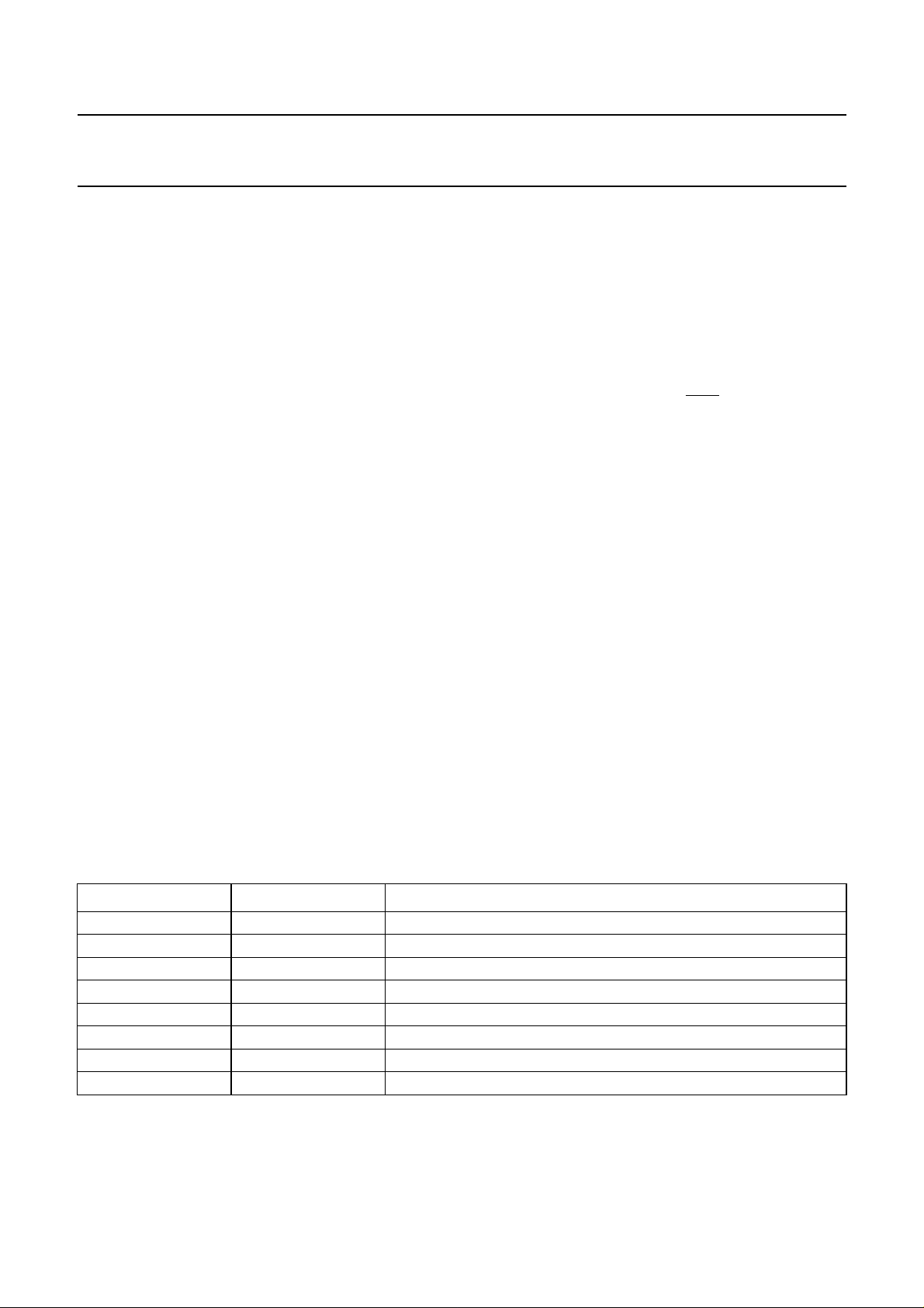
5 BLOCK DIAGRAM
handbook, full pagewidth
V
DDD1
SDA
SCL
INT
RESET
SYN
DMACK
DA1
DA2/EJECT
CS2/SELRQ
IOCS16
1, 14, 24,
41, 59, 68
32
36
37
38
39
40
45
70
71
72
73
DGND
CONTROLLER
V
MICRO-
INTERFACE
DDD2
RCK
SFSY
50, 74 28
HOST INTERFACE
BCKWSDATA
SUB
29 30 31 33 34 35 23 25
DECODER
SERIAL
INTERFACE
ERROR
CORRECTOR
SRAM
CACHE
C2PO TEST1
TEST2
TEST
SAA7380
MEMORY
MANAGER
OSCILLATOR
SAA7380
75-80
2-10
12
11
13
15-22
27
26
RA0 to RA5
RA6 to RA14
RA16/CAS
RA15/RAS
RWE
RD0 to RD7
CRIN
CROUT
42 43 44 69 46 47 48 49
CS1/HEN
HRD
HWR DA0/CMD
IORDY/WAIT/HFBLB
DMARQ/DTEN
SCRST/STEN
IRQ/EOP/HFBC
Fig.1 Block diagram.
1996 Apr 25 4
51-58 60-67
MGE190
HD0 to HD7 HD8 to HD15

Philips Semiconductors Preliminary specification
Error correction and host interface IC for
SAA7380
CD-ROM (ELM)
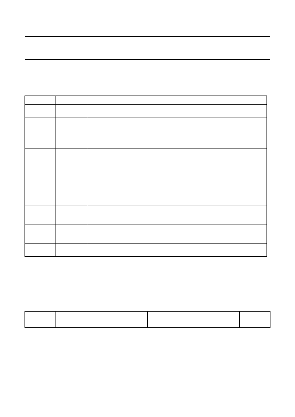
6 PINNING
SYMBOL PIN I/O DESCRIPTION
DGND1 1 − digital ground 1
RA6 2 O buffer RAM address bus output line 6
RA7 3 O buffer RAM address bus output line 7
RA8 4 O buffer RAM address bus output line 8
RA9 5 O buffer RAM address bus output line 9
RA10 6 O buffer RAM address bus output line 10
RA11 7 O buffer RAM address bus output line 11 (SRAM) only
RA12 8 O buffer RAM address bus output line 12 (SRAM) only
RA13 9 O buffer RAM address bus output line 13 (SRAM) only
RA14 10 O buffer RAM address bus output line 14 (SRAM) only
RA15/RAS 11 O buffer RAM address bus output line 15 (SRAM) or RAS (DRAM)
RA16/CAS 12 O buffer RAM address bus output line 16 (SRAM) or CAS (DRAM)
RWE 13 O buffer RAM write enable output
DGND2 14 − digital ground 2
RD0 15 I/O buffer RAM data bus bidirectional line 0
RD1 16 I/O buffer RAM data bus bidirectional line 1
RD2 17 I/O buffer RAM data bus bidirectional line 2
RD3 18 I/O buffer RAM data bus bidirectional line 3
RD4 19 I/O buffer RAM data bus bidirectional line 4
RD5 20 I/O buffer RAM data bus bidirectional line 5
RD6 21 I/O buffer RAM data bus bidirectional line 6
RD7 22 I/O buffer RAM data bus bidirectional line 7
TEST2 23 I test input 2
DGND3 24 − digital ground 3
TEST1 25 I test input 1
CROUT 26 O clock oscillator output
CRIN 27 I clock oscillator input
SFSY 28 I serial subcode input frame sync input
RCK 29 O serial subcode clock output (active LOW)
SUB 30 I serial input for Q-to-W subcode input
BCK 31 I serial interface bit clock input
V
DDD1
WS 33 I serial interface word clock input
DATA 34 I serial data input
C2PO 35 I serial interface flag input
SDA 36 I/O sub-CPU serial data input/output
SCL 37 I sub-CPU serial clock input
INT 38 O sub-CPU open-collector interrupt output
RESET 39 I power-on reset input (active LOW)
SYN 40 I sync signal input from sub-CPU
32 − digital supply voltage 1 (3.3 V)
1996 Apr 25 5
Philips Semiconductors Preliminary specification
Error correction and host interface IC for
SAA7380
CD-ROM (ELM)
SYMBOL PIN I/O DESCRIPTION
DGND4 41 − digital ground 4
CS1/HEN 42 I host interface enable input (active LOW)
HWR 43 I host interface write enable input (active LOW)
HRD 44 I host interface read enable input (active LOW)
DMACK 45 I DMA acknowledge input
IORDY/WAIT/HFBLB 46 O host interface wait output (active LOW); 3-state control
SCRST/STEN 47 O host interface status enable output ATAPI sub-CPU reset signal
(active LOW)
DMARQ/DTEN 48 O ATAPI DMA request host interface data enable output (active LOW);
3-state control
IRQ/EOP/HFBC 49 O host interface end of process flag output ATAPI host interrupt request
(active LOW); 3-state control
V
DDD2
HD0 51 I/O host interface data bus input/output line 0
HD1 52 I/O host interface database input/output line 1
HD2 53 I/O host interface database input/output line 2
HD3 54 I/O host interface data bus input/output line 3
HD4 55 I/O host interface data bus input/output line 4
HD5 56 I/O host interface data bus input/output line 5
HD6 57 I/O host interface data bus input/output line 6
HD7 58 I/O host interface data bus input/output line 7
DGND5 59 − digital ground 5
HD8 60 I/O host interface data bus input/output line 8
HD9 61 I/O host interface data bus input/output line 9
HD10 62 I/O host interface data bus input/output line 10
HD11 63 I/O host interface data bus input/output line 11
HD12 64 I/O host interface data bus input/output line 12
HD13 65 I/O host interface data bus input/output line 13
HD14 66 I/O host interface data bus input/output line 14
HD15 67 I/O host interface data bus input/output line 15
DGND6 68 − digital ground 6
DA0/CMD 69 I host interface data input (active LOW)/command select input host interface
DA1 70 I ATAPI address line input 1
DA2/EJECT 71 I ATAPI address line input 2
CS2/SELRQ 72 I ATAPI chip select input 2
IOCS16 73 O ATAPI 16-bit data select output
V
DDD2
RA0 75 O buffer RAM address bus output line 0
RA1 76 O buffer RAM address bus output line 1
RA2 77 O buffer RAM address bus output line 2
50 − digital supply voltage 2 (5 V)
address line 0
74 − digital supply voltage 2 (5 V)
1996 Apr 25 6
Philips Semiconductors Preliminary specification
Error correction and host interface IC for
CD-ROM (ELM)
SYMBOL PIN I/O DESCRIPTION
RA3 78 O buffer RAM address bus output line 3
RA4 79 O buffer RAM address bus output line 4
RA5 80 O buffer RAM address bus output line 5
handbook, full pagewidth
RA0
75
DDD2
V
IOCS16
74
73
SAA7380
CS2/SELRQ
DA2/EJECT
71
72
DA1
70
DA0/CMD
69
DGND1
RA6
RA7
RA8
RA9
RA10
RA11
RA12
RA13
RA14
RA15/RAS
RA16/CAS
RWE
DGND2
RD0
RD1
RD2
RD3
RD4
RD5
RD6
RD7
TEST2
DGND3
RA2
RA5
RA4
RA3
80
79
78
1
2
3
4
5
6
7
8
9
10
11
12
13
14
15
16
17
18
19
20
21
22
23
24
RA1
77
76
DGND6
68
HD15
67
HD14
66
HD13
65
HD12
64
HD11
63
HD10
62
HD9
61
HD8
60
DGND5
59
HD7
58
HD6
57
HD5
56
HD4
55
HD3
54
HD2
53
HD1
52
HD0
51
V
50
DDD2
IRQ/EOP/HFBC
49
DMARQ/DTEN
48
SCRST/STEN
47
IORDY/WAIT/HFBLB
46
DMACK
45
HRD
44
HWR
43
CS1/HEN
42
DGND4
41
SAA7380
25
26
27
28
29
30
31
32
SUB
TEST1
CRIN
CROUT
SFSY
RCK
BCK
V
Fig.2 Pin configuration.
1996 Apr 25 7
DDD1
33
WS
34
DATA
35
C2PO
36
SDA
37
SCL
38
INT
39
RESET
40
SYN
MGE189

Philips Semiconductors Preliminary specification
Error correction and host interface IC for
CD-ROM (ELM)
6.1 Pin functions
6.1.1 RA0
External memory address signals.
6.1.2 RA16/CAS
External memory RA16 signal if SRAM or, CAS signal if
DRAM.
6.1.3 RA15/RAS
External memory RA15 signal if SRAM or, RAS signal if
DRAM.
6.1.4 RWE
Write output enable signal for external buffer memory. This
is LOW when the SAA7380 wants to write data into the
external memory.
6.1.5 RD0
External buffer memory bidirectional data signals.
TO RA14
TO RD7
SAA7380
6.1.12 C2PO
Error flag from the CD decoder. A HIGH indicates that a
byte has not been corrected by the C2 error corrector and
therefore is not valid. This is taken into account by the
SAA7380 error corrector.
6.1.13 SDA
Sub-CPU bidirectional data signal. This signal forms part
of the 3-wire serial interface between the SAA7380 and the
sub-CPU.
6.1.14 SCL
Sub-CPU sync signal. This signal forms part of the 3-wire
serial interface between the SAA7380 and the sub-CPU.
This signal is used to synchronize data transfers between
the sub-CPU and the SAA7380.
6.1.15 INT
Sub-CPU interrupt signal. This active LOW output signals
to the sub-CPU that the SAA7380 has an interrupt request.
6.1.6 SFSY
Frame sync for the Q-to-W subcode, indicates when
P-channel is available by a HIGH-to-LOW transition.
Frame 0 is also indicated by no transition on this line.
6.1.7
In response to SFSY going LOW data is clocked into the
SAA7380 before each rising edge using this clock output.
6.1.8 SUB
Q-to-W subcode is input in response to
mode or WS in “V4” mode compatible with the SAA7345.
6.1.9 BCK
Bit clock for the serial data input from the CD decoder.
6.1.10 WS
Word clock for the serial data input from the CD decoder.
6.1.11 DATA
Serial data input from the CD decoder. This may be either
2
I
S-bus or EIAJ 16-bit format.
RCK
RCK in 3-wire EIAJ
6.1.16
Forcing this input LOW resets the SAA7380.
6.1.17 SYN
Sub-CPU clock signal. This signal forms part of the 3-wire
serial interface between the SAA7380 and the sub-CPU.
This signal is the sub-CPU driven bit clock used to
synchronize the signals on the SDA line.
6.1.18
In the ATAPI mode this is the host chip select 1 address
signal. In the Sanyo and Oak compatibility modes setting
this input LOW enables the host interface.
6.1.19
This active LOW signal is the host write request.
6.1.20
This active LOW signal is the host read request.
RESET
CS1/HEN
HWR
HRD
1996 Apr 25 8

Philips Semiconductors Preliminary specification
Error correction and host interface IC for
CD-ROM (ELM)
6.1.21 DMACK
This signal is used in the ATAPI and Oak compatibility
modes during DMA transfers. The host pulls this signal
LOW in response to a DMARQ request to indicate that it is
ready to transfer data.
If this signal is not being used then it must be pulled HIGH
for SAA7380 to operate correctly.
6.1.22
In the ATAPI mode this signal is negated to extend the
host transfer cycle of any host register access. It is used in
PIO transfers. When IORDY is not negated it is in a
high-impedance state.
In the Sanyo compatibility mode the function of this signal
depends on the SELRQ input. If SELRQ is HIGH then
WAIT is set LOW to extend the host transfer cycle. If
SELRQ is LOW then WAIT acts as the DRQ signal in a
DMA transfer.
IORDY/WAIT/HFBLB
SAA7380
6.1.25
In the ATAPI mode this active HIGH signal indicates a host
interrupt request. It is asserted when the sub-CPU writes
to the ITRG register and is negated when the host reads
the status register or writes to the command register.
In the Sanyo compatibility mode this signal is set LOW
when the last data byte is transferred to or from the host.
In the Oak compatibility mode this is the Host First Byte
Cycle output and is HIGH while the first byte in the pseudo
16-bit DMA transfer is accessed. It should be used to
inhibit non-DMA transactions while the first byte is latched.
6.1.26 HD0
These are the bidirectional Host Data signals. In the Sanyo
and Oak compatibility modes HD8 to HD15 are never
used.
6.1.27
IRQ/EOP/HFBC
TO HD15
DA0/CMD
In the Oak compatibility mode this signal is the Host First
Byte Latch signal. A rising edge on this signal is used to
latch the first byte in a pseudo 16-bit DMA read. HFBLB
can only be HIGH when pseudo 16-bit DMA transfer mode
is selected.
6.1.23
In the ATAPI or Oak compatibility mode this signal is pulled
LOW to reset the sub-CPU in response to a reset
command from the host.
In the Sanyo compatibility mode this signal is pulled LOW
to signal to the host that status bytes are available for
transfer.
6.1.24
In the ATAPI or Oak compatibility mode this signal is
asserted when the SAA7380 is ready to transfer data
between the host and itself. In ATAPI single word and Oak
DMA transfers this occurs at every word. In ATAPI
multi-word DMA transfers this occurs at the start of the
transfer.
In the Sanyo compatibility mode this signal is pulled LOW
to signal to the host that data bytes are available for
transfer.
SCRST/STEN
DMARQ/DTEN
In the ATAPI mode this is the host Data Address 0 signal.
In the Sanyo and Oak compatibility modes this input
selects between command or data transfers.
6.1.28 DA1
This is the ATAPI Data Address 1 signal.
6.1.29 DA2/ EJECT
In the ATAPI mode this is the Data Address 2 signal. In the
Oak compatibility mode this is the door switch input pin. Its
state is reflected in the TSTAT register.
6.1.30 CS2/SELRQ
In the ATAPI mode this is the Chip Select 2 signal. In the
Oak and Sanyo compatibility mode this is the data transfer
mode select input. It is used to select between PIO and
DMA transfers.
6.1.31 IOCS16
This open-collector signal is used in the ATAPI mode to
signal to the host that a 16-bit data port has been
addressed. It is not activated during DMA transfers.
1996 Apr 25 9

Philips Semiconductors Preliminary specification
Error correction and host interface IC for
CD-ROM (ELM)
7 FUNCTIONAL DESCRIPTION
The SAA7380 is comprised of four main blocks; a CD
player interface, an error corrector, a host interface and a
memory manager. These four blocks operate in parallel.
All receive and send data to the buffer memory via the
memory manager. A 36-kbit on-chip SRAM has been
incorporated to allow high-speed data read operations for
the error corrector.
The SAA7380 performs simultaneous data input buffering,
error correction and host data transfer.
7.1 CD-DSP interface and data input
The input data is synchronized, decoded, and written to
the buffer RAM. The input data format is software
programmable.
The synchronization is achieved using a sync detector and
a sync interpolator. The sync detector detects the sync
pattern in every sector while the interpolator avoids sync
loss when no sync is found. The detector and interpolator
can be individually enabled and disabled under software
control.
After decoding, each full sector of data (2352 bytes)
comprising sync, header, sub-header and parity fields is
written to the buffer RAM.
7.2 Error correction and EDC check
Error correction and detection is performed on each sector
after it is written to the buffer RAM.
SAA7380
7.3 Host interface
The host interface controls data transfers between the
SAA7380 and an external microcontroller. The host
interface can be programmed to operate in three modes.
In the Sanyo compatibility mode the host interface is
functionally compatible with the Sanyo LC89510 block
decoder. In the Oak compatibility mode the host interface
is functionally compatible with the Oak OTI-012 controller
chip in enhanced mode.
In the ATAPI mode the interface meets the ATA Program
Interface specification.
7.4 Subcode channel Q-to-W buffering
As well as buffering the main data, the SAA7380 can also
be used to buffer R-to-W subcode data in buffer memory.
Two buffer modes exist, raw mode and cooked mode. In
the raw mode, data is written to an external RAM without
any processing being performed. In the cooked mode, the
Q-channel data is extracted, the Q-channel CRC is
calculated, the R-to-W data is de-interleaved and the
residues of each R-to-W frame are calculated. These
residues make it easier to correct errors in the data.
7.5 External buffer memory
It is possible to use the SAA7380 with different external
RAM memories. From 0 to 128 kbyte SRAMs or to 16-Mbit
DRAMs are possible. Memories may be nibble or byte
wide (allowing 2, 8 or 16 Mbits). Selection is performed
under software control.
The SAA7380 buffers flag and data of sectors to be
corrected in a 9-bit, 4096 words on-chip RAM memory.
For erasure correction, no external 9-bit memory is
required.
The standard error correction algorithm can be
programmed, and supports Mode 1 and Mode 2, Form 1
and Form 2 discs.
After error correction, an electronic data check is
executed.
When this EDC check is also complete, the sector header
and sub-header is written to 8 header registers, and a
decode complete interrupt is generated.
The microcontroller can then read the decoder status, the
sector header and sub-header and the sector start
address from the SAA7380.
1996 Apr 25 10
Unique to the SAA7380 is its ability to work with partly
defective DRAMs. The SAA7380 offers the possibility to
use a DRAM with bytes in error.
A RAM test is executed under microcontroller control. This
RAM test indicates defective segments to the
microcontroller which keeps a list of which bad sectors to
avoid. The list can be stored in the buffer memory and/or
the microcontrollers own memory.
7.6 Sub-CPU registers
This section describes the registers in the SAA7380. The
operation of the registers varies depending on whether
they are being read from or written to, and the host mode
selected.

Philips Semiconductors Preliminary specification
Error correction and host interface IC for
SAA7380
CD-ROM (ELM)
Table 1 Sub-CPU registers during write
# AR NAME BIT 7 BIT 6 BIT 5 BIT 4 BIT 3 BIT 2 BIT 1 BIT 0
0 00000
1 00001 IFCTRL CMDIEN DTEIEN DECIEN CMDBK DTWAI STWAI DOUTEN SOUTEN
2 00010 DBCL Data Byte Count register bits 7 to 0
3 00011 DBCH Data Byte Count register bits 15 to 8
4 00100 DACL Data Address Counter register bits 7 to 0
5 00101 DACH Data Address Counter register bits 15 to 8
6 00110 DTRG Data Transfer Trigger register
7 00111 DTACK Data Transfer Acknowledge register
8 01000 WAL Write Address register bits 7 to 0
9 01001 WAH Write Address register bits 15 to 8
10 01010 CTRL0 DECEN lookahead E01RQ AUTOQ ERAMRQ WRRQ ECCRQ ENCODE
11 01011 CTRL1 SYIEN SYDEN DSCREN COWREN MODRQ FORMRQ MBCKRQ SHDREN
12 01100 PTL Block Pointer register bits 7 to 0
13 01101 PTH Block Pointer register bits 15 to 8
14 01110
15 01111
16 10000 DACHH mem Data Address Counter register bits 20 to 16
17 10001 WAHH Write Address register bits 20 to 16
18 10010 PTHH Block Pointer register bits 20 to 16
19 10011 SUB_L Subcode Address register bits 7 to 0
20 10100 SUB_H Subcode Address register bits 9 and 8
21 10101
22 10110 INCNF IISmode div 1 div 0 QWmode QWon QWcook RAM test 0
23 10111 MEMS 0 PRIORITY 0 RFRSH WIDTH STATIC CACHE
24 11000 ASTAT ATAPI Status register
25 11001 ITRG Host Interrupt Trigger register
26 11010 ADRADR ATAPI Drive Address register
27 11011 ASAMT ATAPI SAM TAG register
28 11100 DTCTR res. DMAMODE UDMA SUBIEN RDRV TRANT
29 11101 ADRSEL ATAPI Drive Select register
30 11110 AINTR ATAPI Interrupt Reason register
31 11111 AERR ATAPI Error register
ADATA/
SBOUT
RESET reserved HSEL
ATAPI Data register/Status Byte Output register
1996 Apr 25 11

Philips Semiconductors Preliminary specification
Error correction and host interface IC for
SAA7380
CD-ROM (ELM)
Table 2 Sub-CPU registers during read
# AR NAME BIT 7 BIT 6 BIT 5 BIT 4 BIT 3 BIT 2 BIT 1 BIT 0
0 00000
1 00001 IFSTAT CMDI DTEI DECI SUBI DTBSY
2 00010 DBCL Data Byte Count register bits 7 to 0
3 00011 DBCH Data Byte Count register bits 15 to 8
4 00100 HEAD0 Minutes/ File Number
5 00101 HEAD1 Seconds/ Channel Number
6 00110 HEAD2 Frames/ Submode
7 00111 HEAD3 Mode/ Coding Information
8 01000 PTL Block Pointer register bits 7 to 0
9 01001 PTH Block Pointer register bits 15 to 8
10 01010 WAL Write Address register bits 7 to 0
11 01011 WAH Write Address register bits 15 to 8
12 01100 STAT0 CRCOK ILSYNC NOSYNC LBLK USHORT SBLK ERR UCEB
13 01101 STAT1 MINERR SECERR BLKERR MODERR SH0ERR SH1ERR SH2ERR SH3ERR
14 01110 STAT2 RMOD3 RMOD2 RMOD1 RMOD0 MODE FORM RFORM1 RFORM2
15 01111 STAT3 VALST CBLK
16 10000 PTHH Block Pointer register bits 20 to 16
17 10001 WAHH Write Address register bits 20 to 16
18 10010 SUB_L Subcode Address register bits 7 to 0
19 10011 SUB_H Subcode Address register bits 9 and 8
20 10100
21 10101
22 10110
23 10111
24 11000
25 11001 HCON Oak Host Configuration register
26 11010 ACMD ATAPI Command register
27 11011 ASAMT ATAPI SAM TAG register
28 11100 ADCTR ATAPI Device Control register
29 11101 ADRSEL ATAPI Drive Select register
30 11110 AINTR ATAPI Interrupt Reason register
31 11111 AFEAT ATAPI Features register
APCMD/
COMIN
ATAPI packet command data/command input register
SRSTI/
STBSY
DTEN STEN
1996 Apr 25 12
Philips Semiconductors Preliminary specification
Error correction and host interface IC for
CD-ROM (ELM)
7.7 Register Descriptions
7.7.1 SBOUT/ADATA
This is a 12 byte FIFO used to transfer data from the
sub-CPU to the host.
In the Sanyo and Oak compatibility mode writing to this
register starts a status byte transfer. In this mode if the
SOUTEN bit in the IFCTRL register has been set to logic 1,
writing to the SBOUT register sets the STBSY bit to
logic 0. If the STWAI bit is set to logic 0,
immediately set LOW to inform the host computer that the
status byte is ready to be read from.
If the STWAI bit is set to logic 1 and the DTEN bit in the
IFSTAT register is also set to logic 1, both the STEN pin
and the STBSY will go LOW. However, if the STWAI bit is
set to logic 0, and theDTEN bit is set to logic 0, thenSTEN
is held HIGH until the DTEN bit goes HIGH, thereafter it
goes LOW.
STEN is
SAA7380
7.7.2 COMIN/ APCMD
During the ATAPI mode this register is used to read the
program command sent by the host. The program
command can only be received if the appropriate mode
has been selected (see Table 22) and a data transfer has
been started (see DTRG register).
During Sanyo and Oak compatibility modes this register is
a 12 byte FIFO which is used to transfer commands from
the host to the sub-CPU. If reading this register empties
the command FIFO then CMDI is set to logic 1 and further
reads from the register will return FFH.
7.7.3 IFCTRL
The IFCTRL register provides control over the host
interface. Resetting the chip will clear all bits. In the ATAPI
mode, only, bits 7 to 5 have any effect.
Table 3 IFCTRL register bits
BIT NAME DESCRIPTION
7 CMDIEN Enable bits for CMDI, DTEI and DECI. These are interrupt masks, enabling/disabling the
6 DTEIEN
5 DECIEN
4
3
2
1 DOUTEN Data output enable. DOUTEN enables/disables data transfers. When set to logic 0, all
0 SOUTEN Status output enable. SOUTEN enables/disables status byte transfers. When set to
CMDBK Command break enable. If set to logic 0 then the command break function is enabled
DTWAI Data transfer WAIT enable. Setting this bit to logic 0 enables the data WAIT function.
STWAI Status byte transfer WAIT enable. This bit acts in a similar way to the DTWAI bit except it
sub-CPU interrupt pin. They do not affect the bits in the IFSTAT register. If set to logic 1,
the corresponding interrupt is enabled. It should be noted that these masks do not clear
the interrupts.
and if the host writes to the COMIN FIFO then any data or status byte transfers in
progress will be terminated. If set to logic 1 then this operation is disabled. The data
transfer interrupt DTEI is not generated by a command break.
The data WAIT function allows the SAA7380 to delay hardware execution of the data
transfer until a status byte transfer has been completed. Disabling the data WAIT
function allows data transfers to take place independently of status byte transfers.
controls the status WAIT function. The status WAIT function allows the SAA7380 to
delay hardware execution of the status transfer until a data byte transfer has been
completed. Disabling the data WAIT function allows status transfers to take place
independently of data transfers.
data transfers in progress are aborted.
logic 0, the status FIFO register is reset to empty and all status byte transfers in progress
are aborted.
1996 Apr 25 13
Philips Semiconductors Preliminary specification
Error correction and host interface IC for
SAA7380
CD-ROM (ELM)
7.7.4 IFSTAT
The IFSTAT register indicates the state of the host interface. In the ATAPI mode, only bits 7 to 2 have any meaning.
Table 4 IFSTAT register bits
BIT NAME DESCRIPTION
7
6
5
4
3
2
1
0
CMDI Command interrupt. In the ATAPI mode this bit is asserted when the host has written
to the ATAPI command register (see ACMD register) and the drive is selected. It is
also asserted when the host writes the execute drive diagnostic command (90H) to
the ATAPI command register, regardless of whether the drive is selected. It is
negated when the sub-CPU reads the ACMD register. In the Sanyo and Oak
compatibility modes this bit is asserted while there are command bytes waiting in the
COMIN FIFO. It is negated when the COMIN FIFO is empty.
DTEI Data transfer end interrupt. This bit is asserted at the end of data transfer. It is
negated when the sub-CPU writes to the DTACK register. If the ATAPI mode is
selected this bit is also asserted when a program command has been received and
after a sub-CPU memory transfer.
DECI Decoder interrupt. This bit is asserted when a new sector is available. It is negated by
reading the STAT3 register.
SUBI Subcode interrupt. This bit is asserted when a new subcode is available. It is negated
by reading the SUB_H register.
DTBSY Data transfer busy.This bit indicates if a data transfer is taking place. It is asserted by
writing to the DTRG register and is negated at the end of the transfer.
SRSTI/STBSY SRST bit interrupt/status transfer busy. In the ATAPI mode this bit is asserted when
the host writes to the ATAPI device control register and sets the SRST bit. It is
negated when the sub-CPU reads the ADCTR register. It should be noted that if this
bit is asserted in the ATAPI mode then the sub-CPU interrupt will also be asserted.
The SRSTI interrupt cannot be disabled. In the Sanyo and Oak compatibility modes
this bit indicates if a status byte transfer is taking place. It is asserted by writing to the
SBOUT register and is negated when the host has emptied the status FIFO.
DTEN Data transfer and status transfer. These bits reflect the state of the DTEN and STEN
STEN
pins in the Sanyo and Oak compatibility modes. They are updated at the end of a
host read or write.
7.7.5 DBCL AND DBCH
The Data Byte Counter is used by the sub-CPU to control
the number of bytes that are transferred in a data transfer.
In the ATAPI mode all 16 bits are available while in the
Sanyo and Oak compatibility modes only 15 bits are
available with bit 7 of DBCH indicating the state of DTEI
(see Table 4). During memory-to-host data transfers the
data byte counter is decremented after every host read.
During host-to-memory data transfers the data byte
counter is decremented as data is written into external
buffer memory.
1996 Apr 25 14
7.7.6 DACL, DACH AND DACHH
This 21-bit write-only register is used to specify the
external buffer address of the first byte of the data block to
be transferred to the host.
Once the address has been set, it is incremented
automatically as successive bytes are transferred with the
host. It should be noted that pointer operation is
asynchronous from host read/write operation. For this
reason, counter increments are not coincident with host
transfer operations.
Philips Semiconductors Preliminary specification
Error correction and host interface IC for
CD-ROM (ELM)
Bit 7 of the DACHH register specifies which memory is
accessed. If the bit is clear then the address refers to the
external memory, if the bit is set then the address refers to
the 4 kbyte internal memory. The internal memory should
not be accessed during error correction.
This register should be written to before each data transfer
because its value will be undefined at the end of the
previous transfer.
7.7.7 PTL, PTH
This register holds a 21-bit pointer to the external buffer
memory address of the head of the current data block after
correction.
The SAA7380 defines the minute byte in the header to be
at the head of the block, and the 12 sync bytes at the tail
of the block. Each block contained in the buffer is taken to
be 2352 bytes.
The controller can transfer the decoded block back to the
host by copying the address of this register to the DACL,
DACH and DACHH pointers after a decoder interrupt.
When the WRRQ bit in the CTRL0 register is set to logic 1,
this pointer is updated at the sync signal of every
2352 byte clocks.
7.7.8 WAL, WAH
These registers contain a 21-bit address of where raw data
from the drive is written to the external buffer memory. The
pointer is automatically incremented during data transfer.
The pointer should only be read while drive data writes to
the buffer are disabled. If WAHH is written to while drive
data write is enabled, then the new WA value will be used
AND PTHH
AND WAHH
SAA7380
for the first byte of the next sector. The new pointer value
is temporarily stored in the PT register. This cannot be
read after WA has been written to.
7.7.9 DTRG
Writing to this register starts a data transfer. The data
written is discarded.
7.7.10 DTACK
Writing to this register clears the
written is discarded.
7.7.11 HEAD0, HEAD1, HEAD2
These registers are used to hold the header and the
sub-header data of the current block.
To read the header data set, the SHDREN bit in the
CTRL1 register is set to logic 0; to read the sub-header
data, SHDREN is set to logic 1.
If sub-header is selected, the registers will normally hold
data from bytes 20 to 23. However, if the error flag for one
of these bytes is set, then the byte is taken from the first
sub-header field. (bytes 16 to 19.)
The error flags for header and sub-header can be read
from the STAT1 register. No error correction is performed
on header or sub-header.
Header and sub-header registers are valid directly after
decoder interrupt, and as long as the VALST bit in the
STAT3 register is LOW. In all write modes they contain
information on the block whose header is pointed to by
PTL, PTH and PTHH.
DTEI interrupt. The data
AND HEAD3
Table 5 HEAD registers
SHDREN REGISTER CONTENTS
0 HEAD0 MINUTES (byte12)
0 HEAD1 SECONDS (byte 13)
0 HEAD2 FRAMES (byte 14)
0 HEAD3 MODE (byte 15)
1 HEAD0 FILE NUMBER (byte 16 or 20)
1 HEAD1 CHANNEL NUMBER (byte 17 or 21)
1 HEAD2 SUBMODE NUMBER (byte 18 or 22)
1 HEAD3 CODING INFORMATION (byte 19 or 23)
1996 Apr 25 15

Philips Semiconductors Preliminary specification
Error correction and host interface IC for
CD-ROM (ELM)
7.7.12 CTRL0
Resetting the chip sets all the bits in this register to logic 0.
Table 6 CTRL0 register
BIT NAME FUNCTION
7 DECEN Disable decoding = 0; Enable decoding = 1. This bit enables/disables decoding
functions. Disabling the decoding functions also disables the decoder interrupt.
6 lookahead At interrupt PT, header refer to current block = 0; At interrupt PT, header refer to next
block = 1. When this bit is set to logic 1 at decoder interrupt, CMA and header registers
will give information on the next block instead of on the current block. The lookahead
mode was included to provide support for bad RAMs, and to give the CPU better control
on the blocks it wants to read.
5 E01RQ Disable error correction of bytes = 0; Enable correction of CIRC mis-corrections = 1.
Setting this bit to logic 0 instructs the error corrector not to correct bytes flagged as
reliable by the CIRC error corrector.
4 AUTORQ Disable automatic error correction = 0; Enable automatic error correction = 1. Requests
automatic extraction of form bit during Mode 2 correction from sub-header data.
3 ERAMRQ Disable erasure flag use = 0; Enable erasure flag use = 1. When set to logic 1, the
SAA7380 will enable the use of erasure flag information for error correction. When set to
logic 0, the SAA7380 will disable the use of erasure flag information for error correction.
Use of erasure flags must be disabled when the CD-DSP does not output erasure flags
and when the internal buffer RAM is disabled (which is necessary for repeat correction).
2 WRRQ Disable data writes to the buffer and PTL updates = 0; Enables data writes to the buffer
and PTL updates = 1. This bit enables/disables writes from the CD drive into the buffer. It
also enables/disables pointer (PTL, PTH and PTHH) updates each time a block is
received. When WRRQ is set to logic 1, data write will start from the first byte of the next
block onwards. When WRRQ is set to logic 0, repeat correction is enabled. With WRRQ
set to logic 0, the internal buffer RAM is disabled.
1 ECCRQ Disable ECC correction = 0; Enable ECC correction = 1. When ECCRQ is set to logic 1
the blocks received by the SAA7380 will be error corrected before a decoder interrupt is
generated. When ECCRQ is set to logic 0 no corrections are performed. The algorithm
used is a QD, PD, QE, PE algorithm. In a first step, errors are corrected; in a second
step, erasures are corrected. Correction data is read from the on-chip 36 kbit buffer
memory.
0 ENCODE Normal operation = 0; Test mode, do not use = 1, this bit must always be set to logic 0.
SAA7380
1996 Apr 25 16
Philips Semiconductors Preliminary specification
Error correction and host interface IC for
CD-ROM (ELM)
Table 7 Error correction modes
DECEN lookahead WRRQ ECCRQ decoder mode
0 X X X decoder disable; note 1
1000monitor only
1001repeat correction
1010write only
1011real-time correct, normal mode
1110write only, lookahead
1111real-time correct, lookahead
Note
1. Where X = don’t care.
7.7.13 CTRL1
The reset function clears all the flags in this register.
Table 8 CTRL1 register bits
SAA7380
BIT NAME FUNCTION
7 SYIEN Disable sync interpolation = 0; Enable sync interpolation = 1. Enabling SYIEN prevents
loss of synchronization when an error occurs in a sync pattern during data read.
6 SYDEN Disable sync detection = 0; Enable sync detection = 1. Enabling SYDEN synchronizes
the decoder with the sync pattern detected in the input data.
5 DSCREN Descramble disable (audio) = 0; Descramble enable = 1. This bit enables/disables
descrambling. Setting this bit to logic 0 allows reading of raw data on disc, even audio
signals. This bit should be set to logic 1 for CROM data.
4 COWREN CRC with error correction disabled = 0; Detection errors are corrected = 1. This bit
enables/disables rewriting of error bytes in the buffer during error correction. Setting
the bit to logic 0 allows CRC checks without error correction.
3 MODRQ Mode 1 request = 0; Mode 2 request = 1. This bit discriminates Mode 1/Mode 2.
2 FORMRQ Form 1 request = 0; Form 2 request = 1. This bit discriminates Mode 2/Form 1 and
Mode 2/Form 2.
1 MBCKRQ Disable mode check function = 0; Enable mode check function = 1. If the mode
specified in the mode byte does not correspond with the raw data mode bit and this bit
is set to logic 1 then error correction and detection is disabled.
0 SHDREN Header data on registers Head0 to Head3 = 0; Sub-header data on registers
Head0 to Head3 = 1. This bit toggles header and sub-header data between registers
HEAD0 to HEAD3.
1996 Apr 25 17
Philips Semiconductors Preliminary specification
Error correction and host interface IC for
CD-ROM (ELM)
7.7.14 STAT0
Resetting the chip clears all bits in this register.
Table 9 STAT0 register bits
BIT NAME FUNCTION
7 CRCOK Cyclic redundancy check not OK = 0; Cyclic redundancy check OK = 1. Set by the
EDC in accordance with the results of the CRC check.
6 ILSYNC Sync pattern detected at word count 0 to 1174 or 1176 onwards = 1. This bit is set to
logic 1 if the sync pattern in the incoming data is detected between word counts
0 and 1174 or 1176 to infinity, and the decoder has been retimed. Due to the
presence of the cache RAM, it is necessary to stop error correction also when long
blocks have been detected.
5 NOSYNC Sync pattern inserted by sync interpolator not coincident with data sync = 1. This bit
is set to logic 1, if the word counter reaches 1175 and no sync pattern has been
detected in the input data. It indicates that the sync interpolator circuit inserted a
sync.
4 LBLK With SYIEN = 0, no sync found. Data block size has been extended = 1. This bit is
set to logic 1, if the sync interpolator was switched off, and if the sync interpolator
indicated that sync insertion was necessary. This condition causes the block length to
be extended.
3 Reserved
2 SBLK Short block indication = 1. This bit is set to logic 1 if the decoder is not retimed when
a sync pattern is detected in an incorrect word location, and is ignored while the
SYDEN bit is set to logic 0.
1 ERABLK One or more bytes of the block are flagged with C2 flags = 1. This bit is set to logic 1
if one or more bytes of the current block contain erasures as indicated by the C2PO
input.
0 UCEBLK Uncorrectable errors in block = 1. This bit is set to logic 1 when one or more bytes of
the current block remain in error after the error correction process.
SAA7380
7.7.15 STAT1
Resetting the chip clears all bits in this register.
The bits in this register indicate the reliability of data in the HEAD0 to HEAD3 registers. Bits MINERR, SECERR,
BLKERR and MODERR indicate errors in the minutes, seconds, frames and mode bytes in the header of the current
block. Bits SH0ERR to SH3ERR indicate errors in the respective bytes in the sub-header.
Table 10 STAT1 register bits
BIT 7 BIT 6 BIT 5 BIT 4 BIT 3 BIT 2 BIT 1 BIT 0
MINERR SECERR BLKERR MODER SH0ERR SH1ERR SH2ERR SH3ERR
1996 Apr 25 18
 Loading...