

Philips SAA7366T Datasheet

INTEGRATED CIRCUITS
DATA SH EET
SAA7366
Bitstream conversion ADC for
digital audio systems
Preliminary specification
File under Integrated Circuits, IC01
Philips Semiconductors
May 1994
Philips Semiconductors Preliminary specification
Bitstream conversion ADC for
digital audio systems
FEATURES
• Integrated buffers for simple interfacing to analog inputs
• 4 flexible serial interface modes
• Overload detection of digital signal ≥−1 dB amplitude
• Selectable high-pass filter
• 18-bit serial output
• 3.4 to 5.5 V operation of digital part
• Standby mode
• SO24 package
• Small non-critical PCB layout.
GENERAL DESCRIPTION
The SAA7366 is a CMOS cost effective stereo
analog-to-digital converter (ADC) using the Philips
bitstream conversion technique.
QUICK REFERENCE DATA
SAA7366
APPLICATIONS
The device is designed for digital acquisition of analog
audio signals for digital audio systems such as:
• CD-recordable
• Digital Compact Cassette (DCC)
• Digital Audio Tape (DAT).
SYMBOL PARAMETER MIN. TYP. MAX. UNIT
V
DDD
V
DDA
f
i
THD + N total harmonic distortion + noise −−−80 dB
DR dynamic range 90 −−dB
ORDERING INFORMATION
TYPE NUMBER
SAA7366T
Note
1. Plastic small outline package; 24 leads; body width 7.5 mm; (SOT137A); SOT137-1; 1996 Oct 29.
digital supply voltage 3.4 5.0 5.5 V
analog supply voltage 4.5 5.0 5.5 V
clock input frequency 4.608 12.288 13.568 MHz
PACKAGE
PINS PIN POSITION MATERIAL CODE
(1)
24 SO24L plastic SOT137A
May 1994 2
Philips Semiconductors Preliminary specification
Bitstream conversion ADC for
digital audio systems
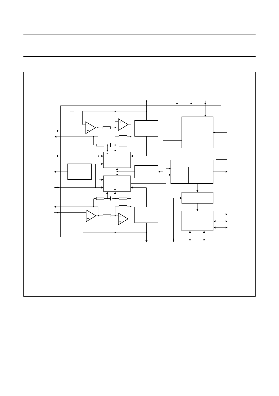
BLOCK DIAGRAM
V
SSA
operational
amplifier
16
BIR
BIL
17
Ω3 k
18
REFERENCE
14
CURRENT
GENERATOR
19
20
21
23 11 24 1
Ω3 k
operational
amplifier operational
V
DACN
I
V
DACP
BOR
REF
BOL
operational
amplifier
Ω10 k
1 pF
SIGMA-
DELTA
MODULATOR
SIGMA-
DELTA
MODULATOR
1 pF
Ω10 k
amplifier
Ω10 k
Ω3 k
Ω3 k
Ω10 k
V
REFR
REFERENCE
VOLTAGE
GENERATOR
TIMING
GENERATOR
REFERENCE
VOLTAGE
GENERATOR
22
SAA7366
TEST2
TEST1
CLOCK
GENERATION
AND
CONTROL
DECIMATION FILTER
STAGE 1
COMB
FILTER
STAGE 2
3 HALF-BAND
FILTERS
HIGH-PASS
FILTER
SERIAL OUTPUT
INTERFACE
STD
SAA7366
210121513
4
CKIN
6
V
SSD
5
V
DDD
3
OVLD
7
SDO
8
SWS
9
SCK
V
DDA
Fig.1 Block diagram.
May 1994 3
V
REFL
HPEN
SLAVE
SFOR
MGA911

Philips Semiconductors Preliminary specification
Bitstream conversion ADC for
SAA7366
digital audio systems
PINNING
SYMBOL PIN DESCRIPTION
SFOR 1 Serial interface output format select. Output format is selected as follows: SFOR
HIGH = Format 1; SFOR LOW = Format 2.
STD 2 Standby mode input (active LOW).
OVLD 3 Overload indication output. This pin indicates whether the internal digital signal is within 1 dB
of maximum. In standby mode this output is high impedance.
CKIN 4 System clock input.
V
DDD
V
SSD
SDO 7 Serial interface data output. In standby mode this output is high impedance.
SWS 8 Serial interface word select signal. In master mode this pin outputs the serial interface word
SCK 9 Serial interface clock. In master mode this pin outputs the serial interface bit clock. In slave
TEST1 10 Test input 1. This pin should be left open-circuit.
HPEN 1 1 High-pass filter enable input. (HPEN HIGH = enabled). If unconnected this pin defaults HIGH.
TEST2 12 Test input 2. This pin should be left open-circuit.
V
SSA
I
REF
V
REFR
BIR 16 Buffer operational amplifier inverting input for right channel.
BOR 17 Buffer operational amplifier output for right channel.
V
DACN
V
DACP
BOL 20 Buffer operational amplifier output for left channel.
BIL 21 Buffer operational amplifier inverting input for left channel.
V
REFL
V
DDA
SLAVE 24 Serial interface operating output mode master/slave select as follows: HIGH = slave mode;
5 Supply for the digital section (3.4 to 5.5 V).
6 Ground supply for the digital section.
select signal. In slave mode this pin is the word select input to the serial interface. In standby
mode this pin is always an input (high impedance).
mode this pin is the input for the external bit clock. In standby mode this output is
high impedance.
13 Ground supply for the analog section.
14 Current reference output node.
1
15
⁄2V
reference generator output for the right channel analog section.
DDA
18 Negative 1-bit DAC reference voltage input, connected to 0 V.
19 Positive 1-bit DAC reference voltage input, connected to +5 V.
1
22
⁄2V
reference generator output for the left channel analog section.
DDA
23 Supply for the analog section.
LOW = master mode. If unconnected the pin will default LOW.
May 1994 4
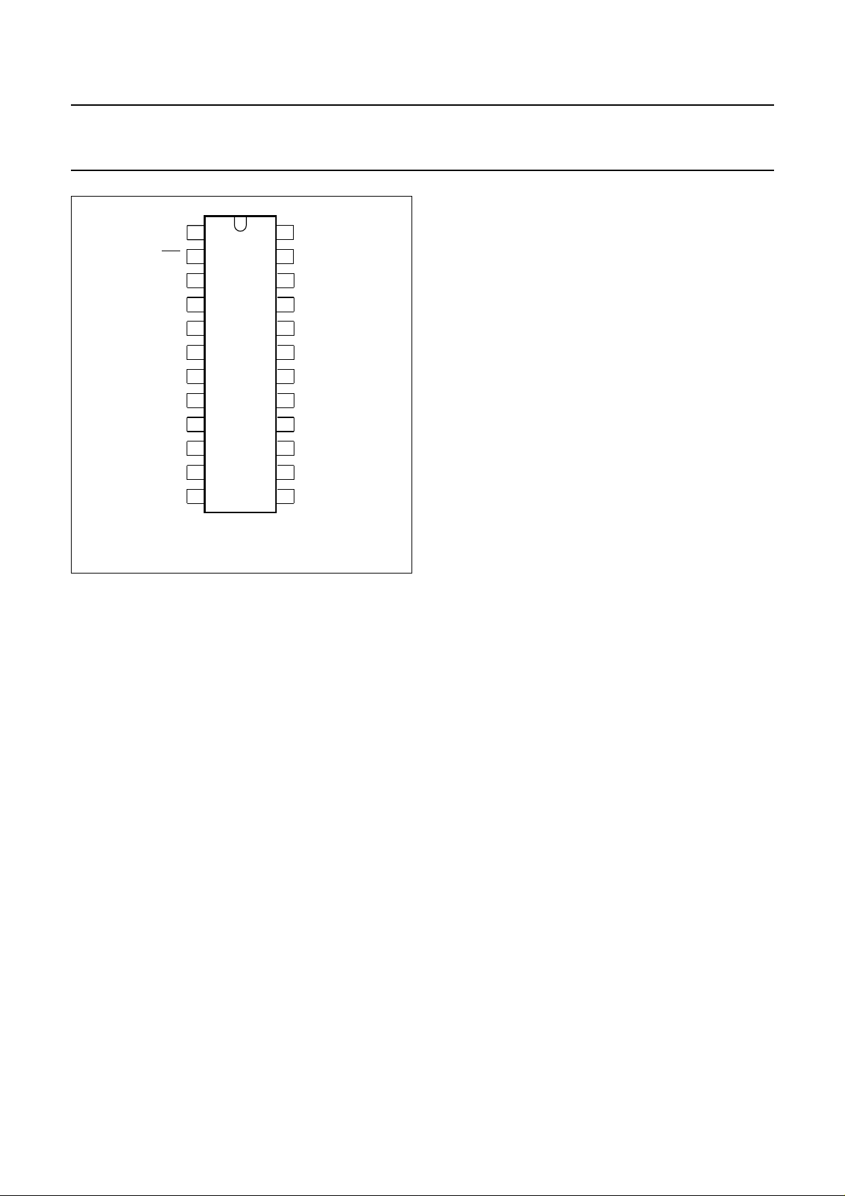
Philips Semiconductors Preliminary specification
Bitstream conversion ADC for
digital audio systems
1
SFOR
2
STD
OVLD
3
CKIN
4
5
V
DDD
V
6
SSD
SDO
SWS
SCK
TEST1
HPEN
TEST2
SAA7366
7
8
9
10
11
12
Fig.2 Pin configuration.
FUNCTIONAL DESCRIPTION
General
The SAA7366 is a bitstream conversion CMOS ADC for
digital audio systems. The conversion is achieved using a
third order Sigma-Delta modulator (SDM), operating at
128 times the output sample frequency (f
oversampling ratio greatly simplifies the design of the
analog input anti-alias filter. In most cases the internal
buffer operational amplifier, configured as a low-pass filter
will suffice. The 1-bit code from the Sigma-Delta modulator
is filtered and down-sampled (decimated) to 1fs in two
stages of filtering. An optional high-pass filter is provided
to remove DC, if required. The device has been designed
with ease of use, low board area and low application costs
in mind.
Clock frequency
The external clock, input on pin CKIN, operates at
256 times f
, which can range from 18 kHz to 53 kHz.
s
Input buffer
Two input buffers are provided, one for each channel, for
signal amplitude matching, signal buffering and anti-alias
filter purposes. These are configured for inverting use.
Access is provided by pins BIL, BIR (inverting inputs) and
BOL, BOR (outputs) for left and right channels
MGA912
24
23
22
21
20
19
18
17
16
15
14
13
SLAVE
V
DDA
V
REFL
BIL
BOL
V
DACP
V
DACN
BOR
BIR
V
REFR
I
REF
V
SSA
). The high
s
SAA7366
respectively. By the choice of feedback component values,
the application signal amplitude can be matched to the
requirements of the ADC. Typically the operational
amplifiers are configured as low-pass filters with a gain
of 1 and a pole at approximately 5fs.
Remark: The complete ADC is non-inverting. Hence a
positive DC input (referenced to V
digital output.
Input level
The overall system gain is proportional V
accurately {V(V
DACP
) − V(V
DACN
ADC input signal amplitude is defined as that amplitude
seen on BOL or BOR, the operational amplifier outputs
(i.e. the input to the Sigma-Delta modulator). Also, the
0 dB input level is defined as that which provides a −1dB
(actually −1.08 dB) digital output, relative to full-scale
swing. This offset provides headroom to accommodate
small random DC offsets without causing the digital output
to clip.
Hence:
()VV
VV
V
0dB()
I
DACP
---------------------------------------------------------------5
The user of the IC should ensure, that when all sources of
signal amplitude variation are taken into account, the
maximum input signal should conform to the 0 dB level. If
not, clipping may occur. In the event that the maximum
signal level cannot be pre-determined, e.g. a live
microphone input, the average signal level should be set
at −10 to−20 dB down. The exact value will depend on the
application and the balance between head room and
operating signal-to-noise ratio.
Behaviour during overload
As defined earlier the maximum input level for normal
operation is 0 dB. If the input level exceeds this value
clipping may occur. Infringements are limited to the
maximum permitted positive or negative values, 2
−217 respectively. If the high-pass filter has been enabled
the clipped output samples may have non-maximum
values due to the removal of the DC content. Input signals
in the range of 0 to 1 dB may or may not be clipped
depending on the values of DC dither and small random
offsets in the analog circuitry.
When using the recommended application circuitry,
clipping will initially be observed on negative peaks due to
the use of negative DC dither.
The maximum level of overload that can be safely
tolerated is application circuit dependent. In the case of the
) will yield a positive
ref
, or more
DDA
)}. For convenience the
()–
DACN
V (RMS)==
17
− 1 or
May 1994 5
Philips Semiconductors Preliminary specification
Bitstream conversion ADC for
digital audio systems
recommended circuit the following applies: the inverting
operational amplifier inputs BIL/BIR are protected from
excessive voltages (currents) by diodes to V
These have absolute maximum ratings of IIK= ±20 mA,
with a safe practical limit of ±2 mA. Given the input resistor
of 10 kΩ, ±2 mA diode current and the operation of the
operational amplifier a maximum signal (applied to the
input resistor) of ±30 V can be handled safely. This level
represents an overload of 26 dB.
During overload the in-band portion of the waveform will be
correctly converted. The out-of-band portion will be limited
as detailed above.
Sigma-Delta modulator
The SAA7366 has two third order Sigma-Delta modulators
with a quantization noise floor of approximately −104 dB.
The scaling of the feedback has been optimized for stable
operation even during overload. Thus with a maximum
signal swing of 0 V to V
on the input the digital output
DDA
remains well behaved, i.e. it does not burst into random
oscillation. During overload the output is simply a clipped
version of the input. The gain of this stage is −4.95 dB.
Decimation filter
DDA
and V
SSA
SAA7366
Table 2 High-pass filter characteristics.
.
Pass band ripple none
Pass band gain 0
Droop at 0.00045f
Attenuation at DC at 0.00000036f
Dynamic range 0 to 0.45f
Serial interface
The serial interface provides 2 formats in both master and
slave modes (see Figs 3 and 4). In both modes the
interface provides up to 18 significant bits of output data
per channel.
During standby mode (
in their high-impedance state. On recovery from standby
the serial data output SDO is held LOW until valid data is
available from the decimation filter. This time depends on
whether the high-pass filter is selected or not as follows:
HPEN = 0; T = 1024/fs, T = 21.3 ms when fs= 48 kHz
HPEN = 1; T = 8192/fs, T = 170.6 ms when fs= 48 kHz
ITEM CONDITION
s
s
s
STD = LOW) all interface pins are
VALUE
(dB)
0.029
>40
116
Decimation from 128fs is performed in two stages. The first
stage is a comb filter, which decimates from 128 to 8f
.
s
The second stage, consists of 3 half-band filters, each
decimating by a factor of 2.
The overall characteristics are given in Table 1.
Table 1 Overall filter characteristics.
ITEM CONDITION
Pass band ripple 0 to 0.45f
0.45 to 0.47f
Stop band >0.55f
s
Dynamic range 0 to 0.42f
Hz ±0.1
s
s
s
VALUE
(dB)
−0.5
−60
110
Gain DC 3.87
High-pass filter
An optional high-pass filter is provided to remove
unwanted DC components. The operation is selected
when HPEN is HIGH. The filter has the characteristics
given in Table 2.
Overload Detection Indication (OVLD)
The OVLD output is used to indicate whenever the data, in
either the left or right channel, is within 1 dB of the
maximum possible digital swing. When this condition is
detected the OVLD output is forced HIGH for at least 512f
cycles (10.6 ms at fs= 48 kHz). This time-out is reset for
each infringement.
Standby mode (
STD)
The STD pin activates a power saving mode when the
device function is not required. This pin can also be used
as a chip enable, as follows.
On a HIGH-to-LOW transition, of the STD pin, the internal
control circuitry starts a timed power-down sequence. This
takes approximately 32 system clock cycles to complete.
Transitions on STD which are shorter than 32 clock cycles
have an indeterminate effect. However, the device will
always recover correctly.
s
May 1994 6
 Loading...