Philips SAA7348G Service Manual

INTEGRATED CIRCUITS
DATA SH EET
SAA7348GP
All Compact Disc Engine (ACE)
Preliminary specification
File under Integrated Circuits, IC22
1997 Jul 11

Philips Semiconductors Preliminary specification
All Compact Disc Engine (ACE) SAA7348GP
CONTENTS
1 FEATURES
2 GENERAL DESCRIPTION
3 ORDERING INFORMATION
4 QUICK REFERENCE DATA
5 BLOCK DIAGRAM
6 PINNING
7 FUNCTIONAL DESCRIPTION
7.1 Analog front-end
7.1.1 Decoder front-end
7.1.2 Servo front end
7.2 Decoder functions
7.3 Servo functions
7.3.1 Signal conditioning
7.3.2 Focus control
7.3.3 Radial control
7.3.4 Off-track counting
7.3.5 Off-track detection
7.3.6 Shock detection
7.3.7 Defect detection
7.3.8 Driver interface
7.3.9 Laser interface
7.4 Subcode interface
7.5 Digital output
7.5.1 Format
7.6 S2B interface
7.7 Audio support
7.7.1 Serial audio data interface
7.8 CD-ROM support
7.8.1 Serial CD-ROM data interface
7.9 Reset
7.10 External ROM support
8 MICROCONTROLLER INTERFACE
8.1 Microcontroller applications registers
8.1.1 CLK generate register (CLKgen)
8.1.2 Port Servo Register (PSR)
8.1.3 Servo Control Register (SCR)
8.1.4 Servo Status Register (STR)
8.1.5 Motor Output QCLV Register (MOQ; address
0XF2H and 0XF3H)
8.1.6 P3 Register
8.1.7 Decoder Status Register (DSR)
8.1.8 Motor Setpoint Register (MSR; address
0XF9H)
8.1.9 Motor Gain QCLV Register (address 0XFAH)
8.1.10 Data Direction Registers (DDR0, DDR2 and
DDR3)
8.1.11 Configuration Control Register (CCR)
8.1.12 A second serial interface
8.1.13 Memory map access to the servo
8.1.14 PLL Registers
8.1.15 DIV17 Register (address 0X9FH)
8.2 Memory map
8.3 Summary of the functions controlled by
decoder registers 0 to F
8.4 Summary of servo commands
8.4.1 Summary of servo command parameters
9 LIMITING VALUES
10 CHARACTERISTICS
10.1 General characteristics
10.2 Subcode interface timing characteristics
10.3 I2S timing characteristics
11 PACKAGE OUTLINE
12 SOLDERING
12.1 Introduction
12.2 Reflow soldering
12.3 Wave soldering
12.4 Repairing soldered joints
13 DEFINITIONS
14 LIFE SUPPORT APPLICATIONS
1997 Jul 11 2

Philips Semiconductors Preliminary specification
All Compact Disc Engine (ACE) SAA7348GP
1 FEATURES
• Focus servo loop
• Radial servo loop
• Built-in access procedure with fast track count
possibilities
• Sledge motor servo loop with pulsed sledge support
• High speed error correction, up to sixteen times
over-speed
• Supports three different over-speed ranges with only
one external crystal
• Lock-to-disc mode
• Full turntable motor control
• Full error correction strategy, t = 2 ande=4
• All standard decoder functions implemented digitally
• Adaptive digital HF equalizer
• FIFO overflow concealment for rotational shock
resistance
• Digital audio interface (EBU), audio and data
• 2 and 4 times oversampling integrated digital filter,
including fs mode
• Audio data peak level detection
• Kill interface for DAC deactivation during digital silence
• All TDA1301 (DSIC2) digital servo functions
• Low focus noise
• Improved playability on ABEX TCD-721R, TCD-725 and
TCD-714 discs
• Automatic closed loop gain control available for focus
and radial loops
• On chip clock multiplier allows the use of 8.4672 MHz
crystal
• S2B serial interface with host controller
• Double speed servo
• Integrated engine controller (high speed embedded
80C51)
• External program support.
2 GENERAL DESCRIPTION
The SAA7348 All Compact Disc Engine (ACE) combines
the functionality of a CD decoder (LO9585), a digital servo
(OQ8868) and a microcontroller core (80C51 based) on a
single chip. It was developed for high speed CD-ROM
applications but, due to the large scale integration, can
also be used in other CD applications. The internal
microcontroller makes it possible to develop other
applications quickly. The microcontroller can operate with
internal or external ROM.
Additional features include:
• High level integration
• Improved communication speed.
3 ORDERING INFORMATION
TYPE NUMBER
NAME DESCRIPTION VERSION
SAA7348GP LQFP100 plastic low profile quad flat package; 100 leads; body 14 × 14 × 1.4 mm SOT407-1
1997 Jul 11 3
PACKAG0E
Philips Semiconductors Preliminary specification
All Compact Disc Engine (ACE) SAA7348GP
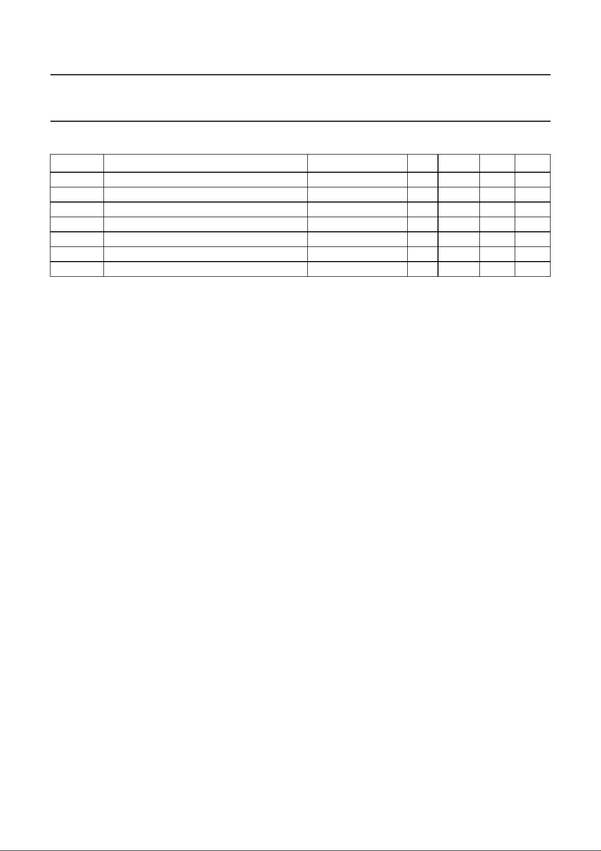
4 QUICK REFERENCE DATA
SYMBOL PARAMETER CONDITIONS MIN. TYP. MAX. UNIT
V
DDD(pads)
V
DDD(core)
V
DDA
I
DD
f
xtal
T
amb
T
stg
Note
1. The analog and digital core supply pins (V
The core and pads can operate at different voltages and should never be connected together directly.
digital supply voltage for pad cells 4.5 5.0 5.5 V
digital supply voltage for the core note 1 3.0 3.3 3.6 V
analog supply voltage note 1 3.0 3.3 3.6 V
supply current n = 8 mode − 90 − mA
crystal frequency 8 8.4672 35 MHz
operating ambient temperature 0 − 70 °C
storage temperature −55 − +125 °C
DDA
and V
DDD(core)
) must be connected to the same external supply.
1997 Jul 11 4
Philips Semiconductors Preliminary specification
All Compact Disc Engine (ACE) SAA7348GP
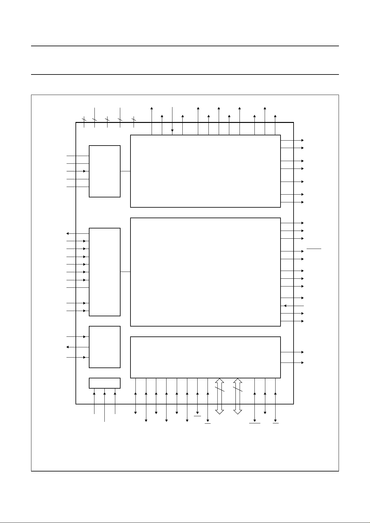
5 BLOCK DIAGRAM
handbook, full pagewidth
MIDLAD
REFLCA
HFIN
REFHCA
I
ref
V
RH
D1
D2
D3
D4
S1
S2
I
refT
FTC
H
FTC
L
V
DDD(core)
HF
V
V
SSA
V
DDA
2 2 2 9 3
(1) (2) (3) (4)
7
8
9
FRONT-END
10
11
SAA7348GP
14
15
16
17
20
21
22
23
24
25
LF
FRONT-END
SSD
V
DDD(pads)
(5)
SBSY RCK VALID
SFSY SUB DAC WCLK DACCLK
92
93
94 95 65 66 67 68 69 62 97 96
DECODER
DIGITAL SERVO
DATA SCLK KILL
DEEM
100
89
71
73
72
91
86
85
84
83
82
74
75
78
79
80
90
98
99
DOBM
SUBQW
MOTOV
MOTOS
FB
C2FAIL
CFLG
FOK
TL
RP
DSDEN
CLO
RA
FO
SL
OTD
DEFI
DEFO
LDON
XTALI
XTALO
SELPLL
(1) Pins 13 and 19.
(2) Pins 12 and 18.
(3) Pins 39 and 88.
(4) Pins 29, 38, 51, 61,
63, 70, 76, 81 and
87.
(5) Pins 52, 64 and 77.
28
27
26
CLOCK
PLL
TEST
1 2 3 30 31 32 33 34 35 36 37 48
TS1 TS3
TS2
R
XD0
T
XD0
INT0
INT1
R
XD1
T
Fig.1 Block diagram.
1997 Jul 11 5
XD1
80C51
8
40 to4753 to
A8 to
A15
AD0 to
AD7
5
TPWM
6
TEN
8
60
49 50
ALE
PSENWREARD
MGK498

Philips Semiconductors Preliminary specification
All Compact Disc Engine (ACE) SAA7348GP
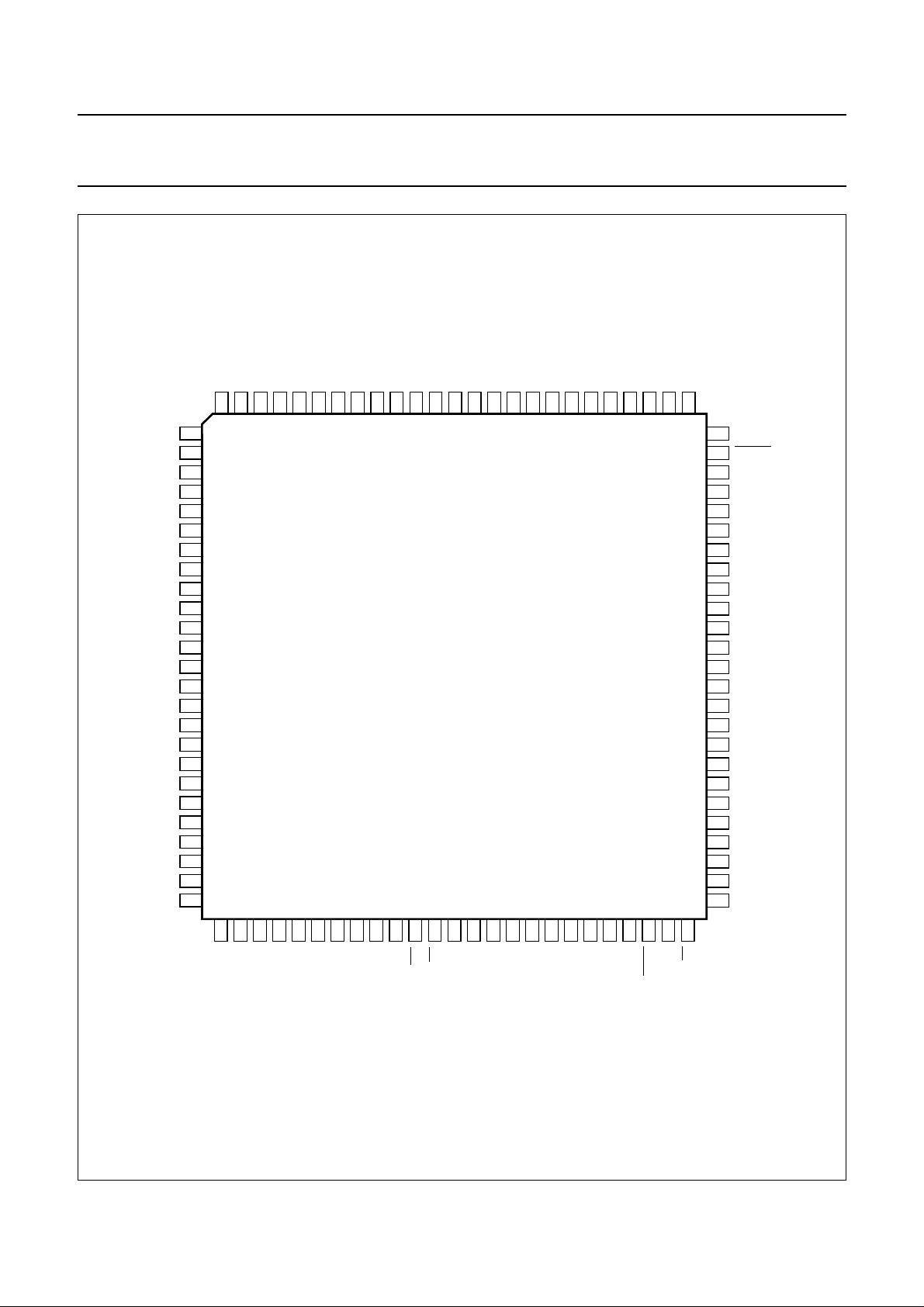
6 PINNING
SYMBOL PIN TYPE
(1)
DESCRIPTION
TS1 1 I test control input; this pin should be tied LOW
TS2 2 I test control input; this pin should be tied LOW
TS3 3 I test control input; this pin should be tied LOW
RST 4 I power-on reset input
TPWM 5 O tray PWM output
TEN 6 O tray enable output
MIDLAD 7 A ladder middle decoupling of High Frequency (HF) ADC
REFLCA 8 A ladder low decoupling of HF ADC
HFIN 9 A HF input
REFHCA 10 A ladder high decoupling of HF ADC
I
ref
V
V
V
SSA1
DDA1
RH
11 A reference current input
12 S analog ground 1 for HF front-end
13 S analog supply voltage 1 for HF front-end (3.3 V)
14 A calibrated reference voltage output from ADC
D1 15 A unipolar current input (central diode signal input)
D2 16 A unipolar current input (central diode signal input)
D3 17 A unipolar current input (central diode signal input)
V
V
SSA2
DDA2
18 S analog ground 2 for LF front-end
19 S analog supply voltage 2 for LF front-end (3.3 V)
D4 20 A unipolar current input (central diode signal input)
S1 21 A unipolar current input (satellite diode signal input)
S2 22 A unipolar current input (satellite diode signal input)
I
refT
FTC
FTC
H
L
23 A current reference, for input range of LF front-end ADCs
24 A fast track counter comparator (+) input
25 A fast track counter comparator (−) input
SELPLL 26 I enables internal clock multiplier PLL
XTALO 27 A crystal output
XTALI 28 A crystal input
V
R
T
SSD1
XD0
XD0
29 S digital ground 1
30 B P3.0
31 B P3.1
INT0 32 B P3.2 (interrupt 0)
INT1 33 B P3.3 (interrupt 1)
R
XD1
T
XD1
34 B P3.4
35 B P3.5
WR 36 B P3.6; active LOW
RD 37 B P3.7; active LOW
V
SSD2
V
DDD1(core)
38 S digital ground 2
39 S digital supply voltage 1 for the core (3.3 V)
A8 40 B P2.0 (address or I/O)
1997 Jul 11 6

Philips Semiconductors Preliminary specification
All Compact Disc Engine (ACE) SAA7348GP
SYMBOL PIN TYPE
(1)
DESCRIPTION
A9 41 B P2.1 (address or I/O)
A10 42 B P2.2 (address or I/O)
A11 43 B P2.3 (address or I/O)
A12 44 B P2.4 (address or I/O)
A13 45 B P2.5 (address or I/O)
A14 46 B P2.6 (address or I/O)
A15 47 B P2.7 (address or I/O)
PSEN 48 B program store enable (pull-up; active LOW)
ALE 49 B address latch enable (pull-up)
EA 50 B external ROM select (active LOW); enhanced hooks
V
SSD3
V
DDD1(pads)
51 S digital ground 3
52 S digital supply voltage 1 for the pads (5 V); pins 26 to 60
AD0 53 B P0.0 (data, address or I/O)
AD1 54 B P0.1 (data, address or I/O)
AD2 55 B P0.2 (data, address or I/O)
AD3 56 B P0.3 (data, address or I/O)
AD4 57 B P0.4 (data, address or I/O)
AD5 58 B P0.5 (data, address or I/O)
AD6 59 B P0.6 (data, address or I/O)
AD7 60 B P0.7 (data, address or I/O)
V
SSD4
61 S digital ground 4
DACCLK 62 T BCC-DAC clock output
V
SSD5
V
DDD2(pads)
63 S digital ground 5
64 S digital supply voltage 2 (level shifter) for the pads (5 V)
VALID 65 T data validity flag; C2 error flag; (3-state)
DAC 66 T serial audio data output to DAC (3-state)
DATA 67 T serial data output to block decoder (3-state)
WCLK 68 T word clock output (3-state)
SCLK 69 T serial bit clock output (3-state)
V
SSD6
70 S digital ground 6
SUBQW 71 O subcode output; Q to W subcode bits
MOTOS 72 T motor output, sign
MOTOV 73 T motor output, value
DSDEN 74 O DSD enable output (active LOW)
CLO 75 O clock output
V
SSD7
V
DDD3(pads)
76 S digital ground 7
77 S digital supply voltage 3 for the pads (5 V); pins 1 to 6 and 65 to 100
RA 78 T radial actuator output
FO 79 T focus actuator output
SL 80 T sledge control output
V
SSD8
81 S digital ground 8
1997 Jul 11 7

Philips Semiconductors Preliminary specification
All Compact Disc Engine (ACE) SAA7348GP
SYMBOL PIN TYPE
(1)
DESCRIPTION
RP 82 OD radial polarity signal (open drain)
TL 83 OD track loss signal (open drain)
FOK 84 OD focus OK signal or decoder measurement signal (open drain)
CFLG 85 OD correction flag output (open drain)
C2FAIL 86 OD indication of correction failure (open drain)
V
SSD9
V
DDD2(core)
87 S digital ground 9
88 S digital supply voltage 2 for the core (3.3 V)
DOBM 89 T EBU bi-phase mark output (externally buffered) (3-state)
OTD 90 O off-track detect
FB 91 OD FIFO boundary, motor overflow (open drain)
SBSY 92 T subcode block sync (3-state)
SFSY 93 T subcode frame sync (3-state)
RCK 94 I subcode clock input
SUB 95 T P to W subcode bits (3-state)
DEEM 96 O deemphasis active output
KILL 97 OD kill output (open drain)
DEFI 98 I defect detector input
DEFO 99 O defect detector output
LDON 100 OD laser drive on output (open drain)
Note
1. Pin type abbreviations: O = Output, I = Input, S = power Supply, A = Analog function, OD = Open Drain,
B = Bidirectional, T = 3-state output. All supply pins must be connected directly to their respective external power
supply voltages.
1997 Jul 11 8
Philips Semiconductors Preliminary specification
All Compact Disc Engine (ACE) SAA7348GP
handbook, full pagewidth
DDD3(pads)
SSD7
V
V
75
CLO
74
DSDEN
MOTOV
73
MOTOS
72
71
SUBQW
V
70
SSD6
SCLK
69
68
WCLK
67
DATA
DAC
66
VALID
65
V
64
DDD2(pads)
V
63
SSD5
DACCLK
62
V
61
SSD4
AD7
60
59
AD6
AD5
58
AD4
57
AD3
56
AD2
55
AD1
54
AD0
53
V
52
DDD1(pads)
V
51
SSD3
TS1
TS2
TS3
RST
TPWM
TEN
MIDLAD
REFLCA
HFIN
REFHCA
I
ref
V
SSA1
V
DDA1
V
RH
D1
D2
D3
V
SSA2
V
DDA2
D4
S1
S2
I
refT
FTC
FTC
DDD2(core)
LDON
DEFO
DEFI
KILL
DEEM
SUB
RCK
SFSY
SBSYFBOTD
99989796959493929190898887868584838281
100
1
2
3
4
5
6
7
8
9
10
11
12
13
14
15
16
17
18
19
20
21
22
23
24
H
25
L
SAA7348GP
DOBM
V
SSD9
V
C2FAIL
CFLG
FOKTLRP
SSD8
SLFORA
V
8079787776
26
XTALO
SELPLL
XTALI
31323334353637383940414243444546474849
RD
SSD1
V
XD0
R
XD0
T
INT0
INT1
XD1TXD1
R
WR
30
29
28
27
Fig.2 Pin configuration.
1997 Jul 11 9
SSD2
V
DDD1(core)
V
A8
A9
A10
A11
A12
A13
A14
A15
PSEN
ALE
50
EA
MGK497
Philips Semiconductors Preliminary specification
All Compact Disc Engine (ACE) SAA7348GP
7 FUNCTIONAL DESCRIPTION
The ACE combines the functionality of a DSICS
(OQ8868), a CD65 (LO9585) and an 80C51-based
microcontroller (83C654). In addition, a large part of the
glue logic has been integrated to help minimize the
number of external components required in CD-ROM
applications.
7.1 Analog front-end
The front-end circuit can be split into two parts:
1. The decoder input (HF front-end)
2. The servo input (LF front-end).
Each is powered by a separate power supply pin pair.
7.1.1 D
ECODER FRONT-END
The EFM signal is fed to the decoder through an ADC,
which is preceded by an AGC stage. In order to make full
use of the digital front-end resolution, the gain control
amplifier should deliver a constant 1.4 V p-p output signal.
The gain range of the AGC is 16 dB and is controlled in
steps of 1.0 dB. The gain of the variable gain amplifier is
controlled by an on-chip digital gain control block. This
block allows for both automatic and microcontroller gain
control.
The internal HF detector is sensitive to any disturbance on
the HF signal; a clean (good signal-to-noise ratio) EFM
signal is necessary since high frequency components can
disturb the HF detector. The input range of the HF
front-end varies from 2.3 V p-p down to 0.35 V p-p. If in the
lower range the signal level is between 25% and 75% of
the ADC range, the HF detector will signal NO HF (In this
range an ADC LSB translates into 5.5 mV, so half the
range equals 175 mV. If the total offset was equal to
6 LSBs, the signal range would be reduced by 2 × 33 mV.
In this case a signal of less than 109 mV would signal NO
HF). To ensure the AGC offset is minimized when the AGC
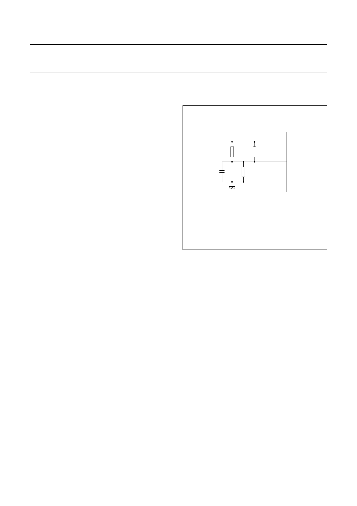
gain is high, it is necessary to connect a resistor divider to
MIDLAD, as shown in Fig.3.
The SAA7348 contains an on-chip digital equalizer and
data slicer. The equalizer is adaptive; actual equalization
depends on the disc speed. The data slicer has a
microcontroller programmable bandwidth. A fully digital
internal PLL is used to regenerate the bit clock.
The bandwidth and equalization of the PLL can be
programmed by the microcontroller. An off-track input is
necessary for certain applications. If the off-track input flag
is HIGH, the SAA7348 will assume that the servo is
following on the wrong track, and will flag all incoming HF
data as incorrect. The off-track input is connected
internally to the servo section.
handbook, halfpage
+3.3 V
820 Ω 820 Ω
10 nF
820 Ω
V
DDA1
MIDLAD
V
SSA1
MGK500
13
7
12
Fig.3 Front-end offset compensation.
7.1.2 SERVO FRONT END
The servo front end contains six current-input ADCs (four
for focus and two for the radial signals). The ADCs do not
require external capacitors, unlike the OQ8868 or CD7
(SAA7370). For high performance radial access, a
comparator input is available for the FTC (Fast Track
Count) signal.
The dynamic range of the ADC input currents can be
adjusted over a range dependent on the value of an
external resistor connected to I
. The maximum input
refT
current for the central and satellite diodes, respectively, is
given below:
I
i(central) max()
I
i satellite()max()
V
is generated internally. The value of VRH is dependent
RH
2.4 106×
----------------------- R
1.2 106×
----------------------- R
µ A()=
IrefT
µ A()=
IrefT
upon the spread of internal capacitors and on the value of
the reference current generated by the external resistor on
I
. Typical input currents for a range of resistance values
refT
are given in Table 1.
1997 Jul 11 10

Philips Semiconductors Preliminary specification
All Compact Disc Engine (ACE) SAA7348GP
Table 1 Typical input currents for a range of values of R
IrefT
TYPICAL CURRENT INPUT RANGE
R
IrefT
(kΩ)
D1, D2, D3, D4
(µA)
(1)
f
= 4.2336 MHz f
sys
S1, S2
(µA)
V
(V)
RH
D1, D2, D3, D4
(µA)
(1)
= 8.4672 MHz
sys
S1, S2
(µA)
V
(V)
RH
200 12.000 6.000 1.891 12.000 6.000 0.946
220 10.909 5.455 1.719 10.909 5.455 0.860
240 10.000 5.000 1.576 10.000 5.000 0.788
270 8.889 4.444 1.396 8.889 4.444 0.698
300 8.000 4.000 1.261 8.000 4.000 0.631
330 7.273 3.636 1.146 7.273 3.636 0.573
360 6.667 3.333 1.051 6.667 3.333 0.526
390 6.154 3.077 0.970 6.350 3.175 0.500
430 5.581 2.791 0.880 −−−
470 5.106 2.553 0.805 −−−
510 4.706 2.353 0.742 −−−
560 4.286 2.143 0.675 −−−
620 3.871 1.935 0.610 −−−
680 3.529 1.765 0.556 −−−
750 3.200 1.600 0.504 −−−
Note
1. f
is always equal to ; see Table 9.
sys
servo clock
------------------------------2
The preset latch command can be used to select this
method of V
automatic adjustment.
RH
Alternatively, the dynamic range of the input currents can
be made dependent on the ADC reference voltage, V
RH
In this case, the maximum input current for the central and
satellite diodes, respectively, is:
I
i(central) max()
I
i(satellite) max()
where f
sys
f
× 1.10× 10⁶–×µA()=
sysVRH
f
× 0.55× 10⁶–×µA()=
sysVRH
= 4.2336 MHz.
VRH can be set to any one of 32 pre-defined levels,
selectable under software control. VRH is initially set to
2.5 V using the preset latch command, then incremented
or decremented one level at a time by repeatedly
resending the same commend.
7.2 Decoder functions
The SAA7348 is a multi-speed decoding device with an
internal phase locked loop clock multiplier. Several
playback speeds can be selected, depending on the
crystal frequency and the internal clock settings;
see Table 2.
The following functions are performed in the decoder
.
block:
• Demodulation (includes sync protection circuit);
converts the 14-bit EFM data and subcode words into
8-bit symbols.
• Subcode data processing.
• Error correction; a t = 2, e = 4 type is used on both C1
(32 symbol) and C2 (28 symbol) frames. The error
corrector can correct up to 2 errors on the C1 level and
up to 4 errors on the C2 level. The error corrector also
contains a flag processor. Flags are assigned to
symbols when the error corrector cannot ascertain if the
symbols are definitely good. C1 generates output flags
that are used by C2. The C2 output flags are used by the
interpolator to conceal uncorrectable errors for audio
output; they are also output via the EBU signal (DOBM)
and the VALID output with I
2
S for CD-ROM applications.
1997 Jul 11 11
Philips Semiconductors Preliminary specification
All Compact Disc Engine (ACE) SAA7348GP
• Motor control; the spindle motor is controlled by a fully
integrated digital servo. Address information from the
internal 8 frame FIFO and disc speed information are
used to calculate the motor control output signals.
Several output modes are supported:
– Pulse density, 2-line (true complement output),
1 × n MHz sample frequency
– PWM-output, 2-line, 22.05 × n kHz modulation
frequency
– CDV motor mode
– Brushless motor control mode.
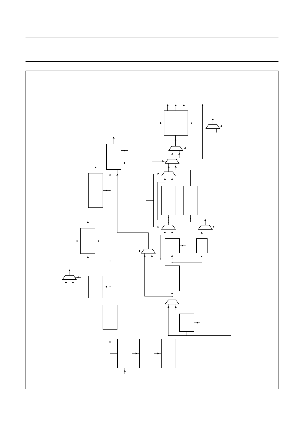
A simplified illustration of the data flow through the
decoder is shown in Fig.4.
Table 2 Decoder playback speeds; note 1
INTERNAL FREQUENCY (MHz)
REGISTER B REGISTER E
67.7376
(2)
50.8032
(2)
33.8688
(2)(3)
16.9344
00XX 0XXX n = 2 n = 1.5 n = 1 −
00XX 1XXX n = 8 n = 6 n = 4 n = 2
01XX 0XXX −−−n=1
01XX 1XXX −−−n=4
10XX 0XXX n = 4 n = 3 n = 2 −
10XX 1XXX n= 16 n = 12 n = 8 −
11XX 0XXX −−−n=2
Notes
1. X = don’t care.
2. With an 8.4672 MHz crystal, and only if SELPLL = 1 (i.e. clock multiplier enabled; see also Section 8.1.1).
3. Can use external 33.8688 MHz crystal.
4. Can use external 16.9344 MHz crystal.
(4)
1997 Jul 11 12
Philips Semiconductors Preliminary specification
All Compact Disc Engine (ACE) SAA7348GP
SCLK
WCLK
DAC
DATA
VALID
DEEM
handbook, full pagewidth
RCK
SUBQW
INTERFACE
MICROCONTROLLER
SBSY
SFSY
SUB
INTERFACE
CD GRAPHICS
reg F
DOBM
EBU
INTERFACE
registers 3, 7 and E
reg A reg E
0 : no pre-emphasis detected
OR reg D = 0xxx
1 : pre-emphasis detected
AND reg D = 1xxx
mode)
s
(1f
1 : reg 3 = xx10
0
1
0 : reg A = xx0x
1 : reg A = xx1x
S-BUS
2
I
INTERFACE
1
0
0
1
1
0
PHASE
COMPENSATION
1
0
FILTER
DIGITAL
reg 3
0 : reg 3 = 101x
(CD-ROM modes)
FILTER
DE-EMPHASIS
1
reg 3
KILL
1
0
1
0
1 : pre-emphasis detected AND reg D = 0xxx
OR reg D = 11xx
MGK499
KILL
0
0
0 : reg 0 = x000/reg 3 = 101x/reg 7 = 00xx/reg E = x0xx
1
0
0 : reg D = xx0x
SUBCODE
INTERFACE
0 : reg D = xx10
1 : reg D = xx11
SUBCODE
PROCESSOR
FIFO
DEMODULATOR
DIGITAL PLL AND
EFM
1997 Jul 11 13
FADE/MUTE/
INTERPOLATE
1
0
ERROR
CORRECTOR
1 : reg 7 = 11xx or 00xx
MONO
reg 7
FUNCTION
Fig.4 SAA7348 decoder function: simplified data flow.

Philips Semiconductors Preliminary specification
All Compact Disc Engine (ACE) SAA7348GP
7.3 Servo functions
7.3.1 S
IGNAL CONDITIONING
The digital codes retrieved from the ADCs are applied to
logic circuitry to obtain various control signals. The signals
from the central aperture diodes are processed to obtain a
normalised focus error signal:
FE
n
D1 D2–
---------------------D1 D2+
D3 D4–
–=
---------------------D3 D4+
where the detector set-up illustrated in Fig.5 is assumed.
For single Foucault focusing, signal conditioning can be
switched under software control such that:
D1 D2–
FE
The error signal, FE
×=
2
n
---------------------D1 D2+
, is further processed by a
n
Proportional Integral and Differential (PID) filter section.
A Focus OK (FOK) flag is generated by means of the
central aperture signal and an adjustable reference level.
This signal is used to provide extra protection for
Track-Loss (TL) generation, drop out detection and the
focus start-up procedure.
The radial or tracking error signal is generated by the
satellite detector signals R1 and R2. The radial error signal
can be formulated as follows:
RE
= (R1 − R2) × re_gain + (R1 − R2) × re_offset
s
where the index ‘s’ indicates the automatic scaling
operation performed on the radial error signal. This scaling
is necessary to avoid non-optimal dynamic range usage in
the digital representation and to reduce the radial
bandwidth spread. Furthermore, the radial error signal will
be free of offset during disc start-up.
The four signals from the central aperture detectors,
together with the satellite detector signals, generate a
track position signal (TPI), which can be formulated as
follows:
TPI = sign [(D1 + D2 + D3 + D4) − (R1 + R2) × sum_gain]
where the weighting factor sum_gain is generated
internally by the SAA7348 during initialization.
handbook, full pagewidth
SATELLITE
DIODE R1
D1
D3
D2
SATELLITE
DIODE R2
single Foucault astigmatic focus double Foucault
SATELLITE
DIODE R1
D1
D2
D3
D4
SATELLITE
DIODE R2
SATELLITE
DIODE R1
D1
D2
D3
D4
SATELLITE
DIODE R2
Fig.5 Detector arrangement.
MBG422
1997 Jul 11 14

Philips Semiconductors Preliminary specification
All Compact Disc Engine (ACE) SAA7348GP
7.3.2 Focus control
The SAA7348 performs the following focus servo function:
• Focus start-up
• Focus position control loop
• Drop-out detection
• Focus loss detection and fast restart
• Focus loop gain switching
• Focus automatic gain control loop.
7.3.3 R
ADIAL CONTROL
The SAA7348 performs the following radial servo
functions:
• Level initialization
• Radial position control loop
• Sledge control
• Tracking control
• Access with or without track loss information
• Radial automatic gain control loop.
7.3.4 O
FF-TRACK COUNTING
The track position signal (TPI) is a flag used to indicate
whether the radial spot is positioned on the track with a
margin of ±0.25 of the track pitch. One of the following
three counting states is selected:
• Protected state
• Slow counting state
• Fast counting state.
7.3.5 O
FF-TRACK DETECTION
The Off-Track Detection (OTD) signal flags off-track
conditions; the polarity of this signal is programmable.
7.3.6 S
HOCK DETECTION
A shock detector can be switched on during normal track
following. Within an adjustable frequency range, it detects
whether disturbances in the radial spot relative to the track
exceed a programmable level. Every time the Radial
tracking Error (RE) exceeds this level, the radial control
bandwidth is switched to twice its original bandwidth and
the loop gain is increased by a factor of 4.
switched off, applied only to focus control, or applied to
both focus and radial controls under software control.
The actions of the circuit can be monitored on the DEFO
pin (active HIGH).
An external defect detector can be added by removing the
connection between DEFO and DEFI (normal operation)
and inserting the necessary circuitry.
7.3.8 D
RIVER INTERFACE
The control signals (pins RA, FO and SL) for the
mechanism actuators are pulse density modulated.
The modulating frequency can be set to either
servo clock
----------------------------- 8
servo clock
or MHz. An analog representation
----------------------------- 4
of the output signals can be generated by connecting a first
order low-pass filter to the outputs.
During reset (i.e. RST pin held HIGH) the RA, FO and SL
pins are high impedance.
7.3.9 L
ASER INTERFACE
The LDON pin (open-drain output) is used to turn the laser
on and off. When the laser is on, the output is high
impedance. The action of the LDON pin is controlled by the
xtra_preset parameter; the pin is automatically driven if the
focus control loop is active.
7.4 Subcode interface
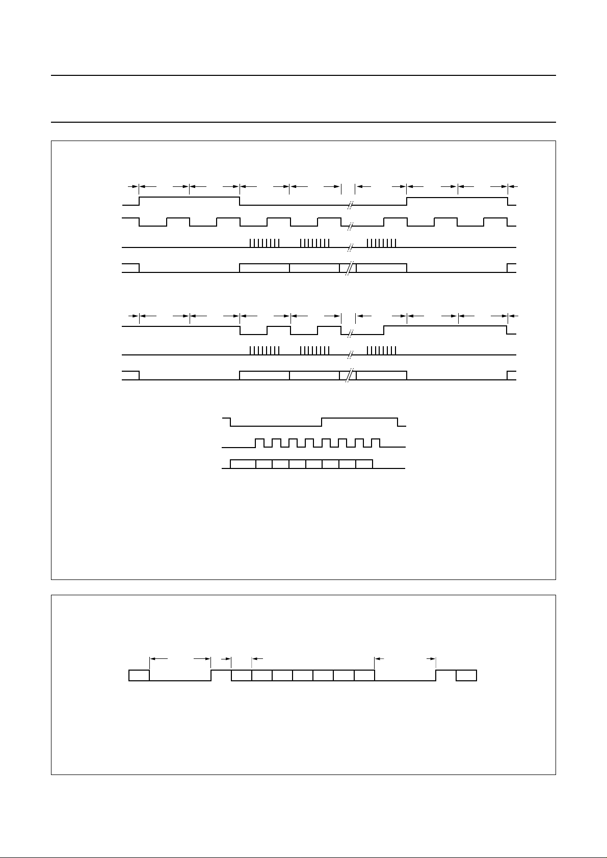
There are two subcode interfaces:
• One which conforms to
“EIAJ CP-2401”
(using SBSY,
SFSY, RCK and SUB) and can be configured as either
a 3- or 4-wire interface. The interface formats are
illustrated in Fig.6.
• An RS232 like format on SUBQW as illustrated in Fig.7.
The subcode sync word is formed by a pause of µs
200
--------- n
minimum. Each subcode byte starts with a 1 followed by
7 bits (Q to W). The gap between bytes can vary
between and µs. Note that SUBQW is not
11.3
----------n
90
-----n
valid in lock-to-disc mode (includes QLLV).
The subcode data is also available at the EBU output
(DOBM).
7.3.7 D
EFECT DETECTION
A defect detection circuit is incorporated into the
SAA7348. If a defect is detected, the circuit can hold all
radial and focus controls. The defect detector can be
1997 Jul 11 15
Philips Semiconductors Preliminary specification
All Compact Disc Engine (ACE) SAA7348GP
handbook, full pagewidth
SBSY
SFSY
RCK
SUB
SFSY
RCK
SUB
SF0 SF1
SF0 SF1 SF2 SF3 SF97 SF0 SF1
SFSY
RCK
SUB
SF2 SF3 SF97 SF0 SF1
P-W P-W P-W
EIAJ 4-wire subcode interface
P-W P-W P-W
EIAJ 3-wire subcode interface
PQRSTUVW
MBG410
Fig.6 EIAJ subcode (CD graphics) interface format.
11.3/n
µs
(1) n = disc speed.
200/n µs
min
W96 1 Q1 R1 S1 T U1 V W1 1 Q2
Fig.7 Subcode format and timing on SUBQW pin.
1997 Jul 11 16
11.3/n µs min
90/n µs max
MGK501

Philips Semiconductors Preliminary specification
All Compact Disc Engine (ACE) SAA7348GP
7.5 Digital output
The AES/EBU signal on pin DOBM is in accordance with
the format defined in
“IEC 958”
. This signal is only
available in the decoder’s CLV modes if audio features are
enabled (not in QCLV modes). Three different modes can
be selected:
• DOBM pin held LOW
• Data taken before concealment, mute and fade (must
• Data taken after concealment, mute and fade (can only
be used for audio modes).
7.5.1 F
ORMAT
The digital audio output consists of 32-bit words
(‘subframes’) transmitted in bi-phasemark code (two
transitions for a logic 1 and one transition for a logic 0).
Words are transmitted in blocks of 384.
always be used for CD-ROM modes)
Table 3 32-bit digital audio output format
FUNCTION BITS DESCRIPTION
Sync 0 to 3 note 1
Auxiliary 4 to 7 not used; normally zero
Error flags 4 CFLG error and interpolation flags when selected by register A
Audio sample
Validity flag
User data
(3)
(4)
Channel status
(2)
(5)
8 to 27 first 4 bits not used (always zero); two’s complement; LSB = bit 12, MSB = bit 27
28 valid = logic 0
29 used for subcode data (Q to W)
30 control bits and category code
Parity bit 31 even parity for bits 4 to 30
Notes
1. The sync word is formed in violation of the bi-phase rule and, therefore, does not contain any data. Its length is
equivalent to 4 data bits. The 3 different sync patterns indicate the following situations:
a) Sync B: word contains left sample (start of a block, 384 words).
b) Sync M: word contains left sample (no block start).
c) Sync W: word contains right sample.
2. Left and right samples are transmitted alternately.
3. Audio samples are flagged (bit 28 = 1) if an error was detected but could not be corrected. This flag remains the same
even if data is taken after concealment.
4. Subcode bits Q to W from the subcode section are transmitted via the user data bit. This data is asynchronous with
the block rate.
5. The channel status bit is the same for both left and right words. Therefore, a block of 384 words contains 192 channel
status bits. The category code is always CD. The bit assignment is shown in Table 4.
1997 Jul 11 17
Philips Semiconductors Preliminary specification
All Compact Disc Engine (ACE) SAA7348GP
Table 4 Channel status bit assignment
FUNCTION BIT DESCRIPTION
Control 0 to 3 copy of CRC checked Q-channel control bits 0 to 3; bit 2 is logic 1 when
copy permitted; bit 3 is logic 1 when recording has pre-emphasis
Reserved mode 4 to 7 always zero
Category code 8 to 15 CD: bit 8 = logic 1, all other bits = logic 0
Clock accuracy 28 and 29 set by register A:
10 = class 1 crystal (<50 ppm)
00 = class 2 crystal (<1000 ppm)
01 = class 3 crystal (>1000 ppm)
Remaining 16 to 27 and 30 to 191 always zero
7.6 S2B interface
This interface is in accordance with the
Description”
. It's a serial interface with a high level
“S2B Interface
command set for controlling a CD-ROM engine.
7.7 Audio support
Audio support consists of several parts:
• Serial data interface.
• Deemphasis control (DEEM). This signal is HIGH if the
subcode info of a track defines it to be recorded with
deemphasis.
• Kill control (KILL). This signal tests for digital silence in
the right and left channel before the digital filter.
The output is switched active LOW if silence has been
detected for at least 250 ms, if mute is active, or in
CD-ROM modes.
• Output clock for BCC-DAC applications (DACCLK).
• Oversampled output. The SAA7348 contains a
2 to 4 times oversampling IIR (Infinite
Impulse-Response) filter, and a selectable deemphasis
filter (if the de-emphasis signal is selected to come out
of DEEM then the filter is bypassed; see Table 31).
• Concealment, mute, attenuation and fade. In audio
modes a 1-sample linear interpolator becomes active if
a single sample is flagged as erroneous; left and right
channels have independent interpolators. A digital level
converter performs the following functions:
– soft mute (signal reduced to 0 in a maximum of
128 steps)
– full-scale (signal ramped back to 0 dB level)
– attenuation (signal scaled by −12 dB)
– fade (activates a 128 stage counter which allows the
signal to be scaled up or down in 0.07 dB steps)
– peak detector (measures highest audio level;
absolute level for left and right channels; the 8 MSBs
of each are output in the Q-channel data).
• Mono output selection. Either channel can be selected
to be output over both left and right channels.
7.7.1 S
ERIAL AUDIO DATA INTERFACE
The serial data interface can be switched between two
modes: Philips I2S and the EIAJ format.
In each case, the serial data is transferred through a 3-wire
interface. The I2S signal contains three components:
WCLK (word select), SCLK (serial clock) and DAC (serial
data). The polarity of WCLK and of the data can be
inverted.
The oversampling frequency and format are selected as
shown in Table 5. The serial data output is separate from
the CD-ROM output. In CD-ROM mode the DAC serial
data output pin will be muted.
Table 5 Oversampling frequency select
MODE
I2S18 4f
EIAJ 18 4f
NUMBER
OF BITS
SAMPLE FREQUENCY
18 2f
16 f
18 2f
18 f
16 4f
16 2f
16 f
s
s
s
s
s
s
s
s
s
1997 Jul 11 18
 Loading...