

Philips saa7346 DATASHEETS

INTEGRATED CIRCUITS
DATA SH EET
SAA7346
Shock absorbing RAM addresser
Preliminary specification
File under Integrated Circuits, IC01
Philips Semiconductors
July 1994
Philips Semiconductors Preliminary specification
Shock absorbing RAM addresser SAA7346
FEATURES
• Absorbs shocks from x, y and z directions
• Absorbs rotational shocks
• Absorbs multiple shocks per second
• Interfaces directly to compact disc decoders SAA7345,
SAA7347 and SAA7370
• Multi-speed I2S-bus input with single-speed
I2S-bus output
• Controls 1 or 4 MBit of external Dynamic Random
Access Memory (DRAM)
• Easy serial interface for communication with common
microcontrollers
• Software selectable shock detectors
• By-pass/power-down mode
• Kill interface for DAC deactivation
• Can be used for:
– ‘sampling’ part of a disc
– to reduce access pauses between jumps
– to deliver a programmable delay
– to generate a fixed audio rate from Constant Angular
Velocity (CAV) discs.
GENERAL DESCRIPTION
The SAA7346 can be used to make a CD player
insensitive to shocks. To do this, SAA7346 operates
closely with a standard 1 Mbit or 4 Mbit DRAM. Audio data
is stored inside the DRAM and during shocks the data of
the DRAM can be played. The SAA7346 functions as a
customized DRAM controller with serial I/O and on-board
shock detectors.
QUICK REFERENCE DATA
SYMBOL PARAMETER MIN. TYP. MAX. UNIT
V
DD
I
DD
f
clk
f
i(clk)
f
o(clk)
T
amb
T
stg
supply voltage 3.3 5.0 5.5 V
supply current − 12 − mA
clock frequency − 16.9344 − MHz
I2S input word clock frequency 44.1 88.2 176.4 kHz
I2S output word clock frequency 44.1 88.2 176.4 kHz
operating ambient temperature −40 − +85 °C
storage temperature −65 − +150 °C
ORDERING INFORMATION
PACKAGE
TYPE NUMBER
PINS PIN POSITION MATERIAL CODE
SAA7346H 44 QFP
(1)
plastic SOT307-2
Note
1. When using reflow soldering it is recommended that the Dry Packing instructions in the
Pocketbook”
are followed. The pocketbook can be ordered using the code 9398 510 34011.
“Quality Reference
July 1994 2
Philips Semiconductors Preliminary specification
Shock absorbing RAM addresser SAA7346
BLOCK DIAGRAM
handbook, full pagewidth
DD2
WCO
32, 30, 28,
26, 25, 27,
29, 31, 33,
DD1
V
34
V
A0
to
A9
RESET
TMS
14
8
SDI
WCI
SCLI
345
2
I S
INPUT
SAA7346
CFLG
KILL
D0 to D3
121319 21 20 22 23 44
DATA
MULTIPLEXER
WRITE
POINTER
REGISTER
KILLOUT
42
to
39
MULTIPLEXER
S_NSF
ADDRESS
SDO
SCLO
2
I S
OUTPUT
READ
POINTER
SICL
SIDA
SILD
V
16
15
17
MONITOR
CONTROLLER
RAS
SS1
MICROCONTROLLER
DETECTORS
24
V
SS2
INTERFACE
SHOCK
9
SSD
OTD
1211 3538373643
RSB
Fig.1 Simplified SAA7347 block diagram.
CAS
WE
OE
TIMING
CLKIN
107
RCD2
6
18
MGB429
CONFIG
FILL
July 1994 3
Philips Semiconductors Preliminary specification
Shock absorbing RAM addresser SAA7346
PINNING
SYMBOL PIN DESCRIPTION
CFLG 1 correction flag input from CD decoder
KILL 2 kill input
SCLI 3 multi-speed I
WCI 4 multi-speed I
SDI 5 multi-speed I
CONFIG 6 external DRAM select input; HIGH 4 Mbit, LOW 1 Mbit
CLKIN 7 16.9344 MHz system clock input
TMS 8 test mode select input; active HIGH
OTD 9 on/off track detector input
RCD2 10 DRAM read cycle divide-by-2 input; active HIGH
SSD 11 shock detected output; active HIGH when shock is detected
RSB 12 rotational shock busy output; active HIGH when rotational shock is detected
S_NSF 13 synthetic new subcode frame output
RESET 14 reset enable input; active LOW
SIDA 15 microcontroller interface input/output data line
SICL 16 microcontroller interface clock input
SILD 17 microcontroller interface
FILL 18 FIFO write enable output; active HIGH
KILLOUT 19 open drain output; active LOW; when in by-pass mode KILLOUT equals KILL
SDO 20 I
SCLO 21 I
WCO 22 I
V
V
DD1
SS1
23 supply voltage 1
24 supply ground 1
2
S data output
2
S bit clock output
2
S word clock output
A4 25 DRAM address bus output 4
A3 26 DRAM address bus output 3
A5 27 DRAM address bus output 5
A2 28 DRAM address bus output 2
A6 29 DRAM address bus output 6
A1 30 DRAM address bus output 1
A7 31 DRAM address bus output 7
A0 32 DRAM address bus output 0
A8 33 DRAM address bus output 8
A9 34 DRAM address bus output 9
OE 35 DRAM enable output; active LOW
RAS 36 DRAM row address strobe output; active LOW
CAS 37 DRAM column address strobe output; active LOW
WE 38 DRAM write enable output; active LOW
2
S bit clock input
2
S word clock input
2
S data input
read/write input
July 1994 4
Philips Semiconductors Preliminary specification
Shock absorbing RAM addresser SAA7346
SYMBOL PIN DESCRIPTION
D3 to D0 39 to 42 DRAM data bus inputs/outputs
V
V
SS2
DD2
43 supply ground 2
44 supply voltage 2
handbook, full pagewidth
CFLG
KILL
SCLI
WCI
SDI
CONFIG
CLKIN
TMS
OTD
RCD2
SSD
DD2
SS2
V
V
44
43
1
2
3
4
5
6
7
8
9
10
11
12
13
RSB
S_NSF
D0
D1
41
42
14
15
SIDA
RESET
D2
D3WECASOERAS
40
39
SAA7346
16
17
SILD
SICL
38
18
FILL
37
36
20
19
KILLOUT
SDO
35
21
SCLO
A9
34
22
WCO
33
32
31
30
29
28
27
26
25
24
23
MGB430
A8
A0
A7
A1
A6
A2
A5
A3
A4
V
V
SS1
DD1
Fig.2 Pin configuration.
FUNCTIONAL DESCRIPTION
2
S input/output interfaces
I
The SAA7346 contains an asynchronous serial input and
a serial output interface. The serial operation of the
interfaces is under hardware control of the external
circuitry and uses the I2S protocol. The output presents a
continuous clock signal SCLO (typically 2.8224 MHz)
which is divided from the system clock, and a word select
signal WCO, typically 44.1 kHz (fs), which is used to
distinguish between right and left channels. When in
by-pass mode WCO and SCLO are the same as the input
interface signals WCI and SCLI, enabling data to pass
through the SAA7346. Since the serial input port is
asynchronous the device is independent of the CD
July 1994 5
decoder clock speed and enables the word clock to vary
from 1.1 × f
to 4 × fs (typically 2 × fs). This is a requirement
s
of any electronic shock absorbing system since the disc
must be rotating faster than usual to assure the FIFO is full
to absorb a shock. The falling edge of WCO indicates the
start of a new transfer. Data is exchanged over the
SDI and SDO pins. The SAA7346 is compatible with a
variety of DAC ICs.
New subcode frame regeneration
The SAA7346 has a digital phase-locked loop (PLL)
system which decodes the F1 and F6 flags, from the first
1-bit signal generated by the CD decoder correction flag
output shown in Fig.3. The F1 flag is the absolute time
sync signal of the New Subcode Frame (NSF). It relates
Philips Semiconductors Preliminary specification
Shock absorbing RAM addresser SAA7346
the position of the subcode-sync to the audio data. This
signal determines the accuracy with which the SAA7346
sews audio data together after a shock. When the CD
decoder preforms a jump the NSF will be missed. The PLL
system will insert the missing pulse. The resulting signal is
the S_NSF which can be used as a time out for reading the
handbook, full pagewidth
CFLG
11.3
µs
F1 F2 F3 F4 F5 F6 F7 F1
Fig.3 CFLG input timing diagram.
0.37 ms
handbook, full pagewidth
S_NSF
subcode from the decoder shown in Fig.4. The S_NSF is
available externally and the NSF flag can be read via the
serial microcontroller interface. The F6 flag indicates at
least one hold has occurred in the decoder’s error
corrector and interpolator. The shock processor uses this
signal to evaluate whether a shock has occurred.
45.4 µs
MGA370
6.6 ms
NSF
Fig.4 S_NSF output timing diagram; n = 2.
Shock processor
The shock processor determines whether a shock has
occurred by processing all the shock detectors. The
SAA7346 will enter shock mode and set SSD when the:
•µCsd flag is set by the microcontroller in the command
register
• OTD input is active while the jmp_bz flag is not set
• RSB output is set while the e_rot_sd flag is set
• NSF pulse is lost and the full flag is not read by the
microcontroller from the status register.
When the target position has been found the
microcontroller should set the PFB flag in the command
register. The SAA7346 will respond by clearing the SSD
flag and start refilling. If CFLG still indicates a hold, the
MGB431
Variable
NSF is set until read
by the microcontroller
decoder is rolling out of its FIFO. RSB will be set which
sets SSD again thus the FIFO will not start refilling. The
microcontroller should jump one track back and look for
the correct target position again. When the motor speed is
stable and the decoder does not roll out of its FIFO, the
audio data will be glued together.
SSD will be reset whenever the microcontroller sets PFB
or the flush flags in the command register, or when the
FIFO empties while the echo flag is LOW. Note if the
microcontroller wants SSD to be clear for a while the shock
detectors should be inhibited.
FIFO controller and monitor
The SAA7346 uses a state machine to control and monitor
the conditions of the FIFO shown in Fig.5.
July 1994 6

Philips Semiconductors Preliminary specification
Shock absorbing RAM addresser SAA7346
handbook, full pagewidth
SSD and
(NSF + S_NSF)
flush + reset +
(empty and echo)
HOLD
HOLD
first nibble full
6
PFB
5
SSD
PFB
Fig.5 State machine flow diagram.
During normal operation the FIFO will fill up because
writing is carried out twice as fast as reading; this is the fill
mode. If the FIFO is full the monitor will detect and set the
full flag. At the same time the fill flag will be reset thus
preventing audio data from being written in to the FIFO.
When the microcontroller reads the full flag from the status
register, the servo control should jump back one track. The
microcontroller enters a wait loop until the same absolute
time subcode frame turns by again; this is the hold mode.
When the spot is found again the microcontroller should
set the PFB flag in the command register and the
SAA7346 will resume writing to the DRAM. While in fill
mode the write pointer address is saved at the end of each
subcode frame. When the player exists hold mode it
restores the saved address and continues writing after the
last sample.
RESET
0
FILL
1
SHOCK
7
HOLD
4
reset and sowflush + reset
SSD
SSD
flush + reset
SSD
first nibble
FILL
2
FILL
3
NSF +
S_NSF
MGB432
When a shock is detected the SAA7346 will enter shock
mode. The shock mode will last until the PFB is set by the
microcontroller or the FIFO is flushed, reset or runs empty.
Microcontroller interface
The SAA7346 has a 3-line microcontroller interface which
is compatible with TDA1301, TDA1303 and SAA7345.
W
RITING DATA TO THE SAA7346
The SAA7346 command register is shown in Table 1. This
can be written to via the microcontroller interface as shown
in Fig.6. The command register flags functions are shown
in Table 2.
Table 1 SAA7346 microcontroller interface registers.
REGISTER BIT 7 BIT 6 BIT 5 BIT 4 BIT 3 BIT 2 BIT 1 BIT 0
Command flush bypass echo jmp_bz otd_p e_rot_sd µCsd PFB
Status Lm Lm1 FRM_ER NSF full empty SSD fill
July 1994 7

Philips Semiconductors Preliminary specification
Shock absorbing RAM addresser SAA7346
Table 2 Command register flag functions.
COMMAND DESCRIPTION
Flush Flush, when set, will empty the FIFO, reset the read and write pointer addresses. Then writing will
resume to the FIFO. Flag reset automatically.
Bypass Bypass, when set, will power down the SAA7346. The I2S interface passes input to output directly.
The parallel interface port controls RAS, CAS, WE and OE which are pulled HIGH. KILL passes
directly to KILLOUT. When exiting by-pass mode the FIFO is automatically flushed.
Echo Echo, when set, will cause the FIFO contents to be continuously played until the correct position is
found again.
jmp_bz Jump busy, when set, indicates a jump is being preformed. The OTD shock detector input will be
disabled. After the jump has finished the flag should be reset by a write.
otd_p OTD polarity enable. Enables the polarity of the OTD input to be switched from active HIGH set,
active LOW not set.
e_rot_sd Enable rotational shock detection, when set, will detect shocks whenever the decoder rolls out of its
internal FIFO.
µCsd Microcontroller shock detected is set when the microcontroller has detected a shock.
PFB Position Found Back, when set, indicates that the microcontroller has found the absolute time frame
after a shock or hold cycle. The audio data will sew together and the flag reset automatically.
handbook, full pagewidth
SICL
SILD
SIDA
B7 B6 B5 B4 B3 B2 B1 B0
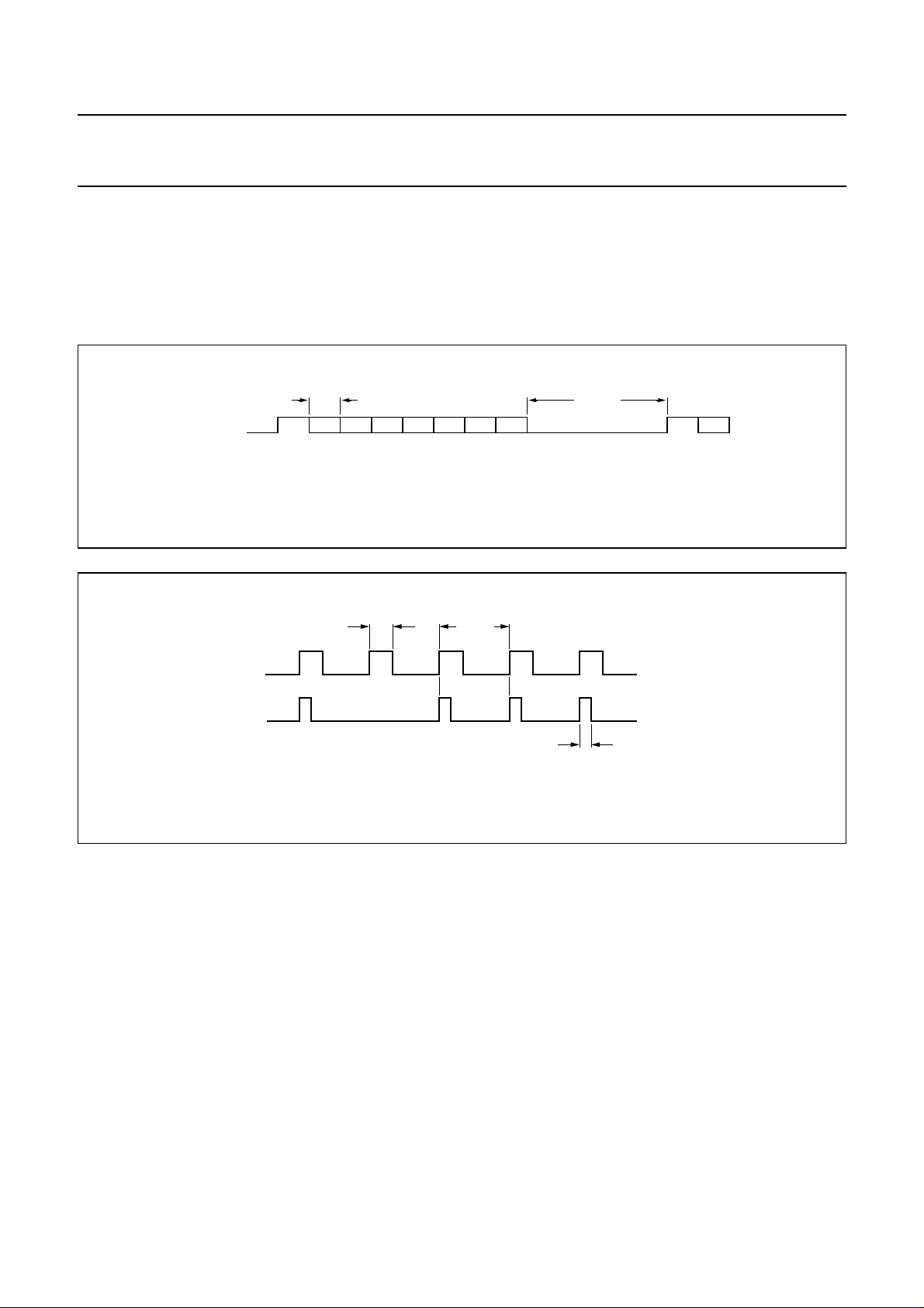
Fig.6 Microcontroller WRITE timing.
Writing operation sequence:
• SILD is held HIGH by the microcontroller.
• Microcontroller data is clocked into the internal
command register on the LOW-to-HIGH clock transition
of SICL.
• SILD is pulled LOW by the microcontroller to latch-in
data to the command register.
• SICL and SILD are pulled HIGH by the microcontroller
to indicate that communications have finished.
MGB433
R
EADING STATUS OF SAA7346
The SAA7346 has a status register shown in Table 1. This
can be read via the microcontroller interface shown in
Fig.7. The internal status signals are made available on
the SIDA pin and are shown in Table 3.
July 1994 8
 Loading...