

Philips SAA7345ZP Datasheet

DATA SH EET
Product specification
Supersedes data of 1996 Jan 09
File under Integrated Circuits, IC01
1998 Feb 16
INTEGRATED CIRCUITS
SAA7345
CMOS digital decoding IC with
RAM for Compact Disc

1998 Feb 16 2
Philips Semiconductors Product specification
CMOS digital decoding IC with RAM for
Compact Disc
SAA7345
FEATURES
• Integrated data slicer and clock regenerator
• Digital Phase-Locked Loop (PLL)
• Demodulator and Eight-to-Fourteen Modulation (EFM)
decoding
• Subcoding microcontroller serial interface
• Integrated programmable motor speed control
• Error correction and concealment functions
• Embedded Static Random Access Memory (SRAM) for
de-interleave and First-In First-Out (FIFO)
• FIFO overflow concealment for rotational shock
resistance
• Digital audio interface [European Broadcasting Union
(EBU)]
• 2 to 4 times oversampling integrated digital filter
• Audio data peak level detection
• Versatile audio data serial interface
• Digital de-emphasis filter
• Kill interface for Digital-to-Analog Converter (DAC)
deactivation during digital silence
• Double speed mode
• Compact Disc Read Only Memory (CD-ROM) modes
• A single speed only version is available
(SAA7345GP/SS).
GENERAL DESCRIPTION
The SAA7345 incorporates the CD signal processing
functions of decoding and digital filtering. The device is
equipped with on-board SRAM and includes additional
features to reduce the processing required in the analog
domain.
Supply of this Compact Disc IC does not convey an implied
license under any patent right to use this IC in any
Compact Disc application.
QUICK REFERENCE DATA
ORDERING INFORMATION
SYMBOL PARAMETER MIN. TYP. MAX. UNIT
V
DD
supply voltage 3.4 5.0 5.5 V
I
DD
supply current − 22 50 mA
f
xtal
crystal frequency 8 16.9344 or
33.8688
35 MHz
T
amb
operating ambient temperature −40 − +85 °C
T
stg
storage temperature −55 − +125 °C
TYPE
NUMBER
PACKAGE
NAME DESCRIPTION VERSION
SAA7345GP QFP44 plastic quad flat package; 44 leads (lead length 2.35 mm); body
14 × 14 × 2.2 mm
SOT205-1
1998 Feb 16 3
Philips Semiconductors Product specification
CMOS digital decoding IC with RAM for
Compact Disc
SAA7345
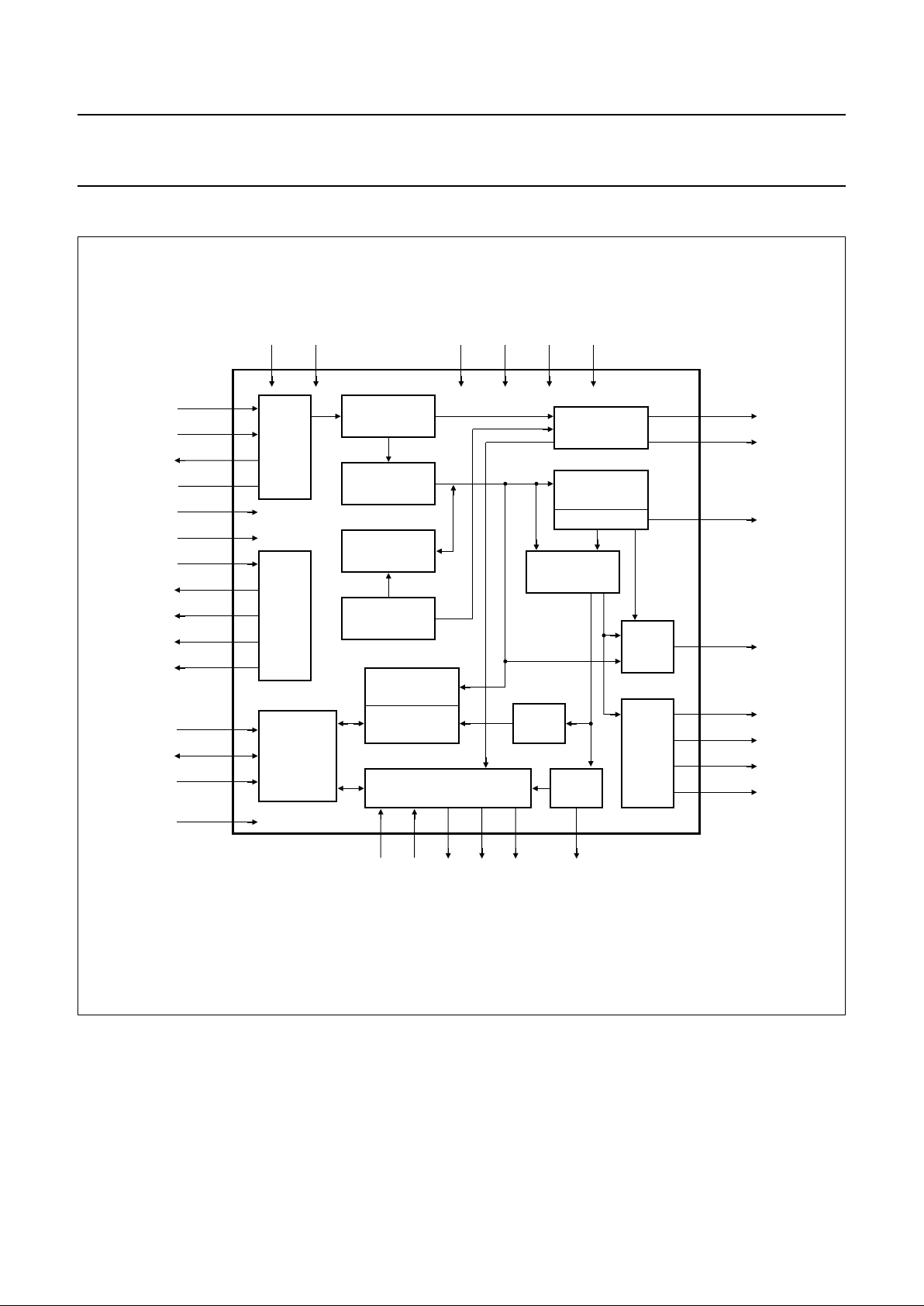
BLOCK DIAGRAM
Fig.1 Block diagram.
MGA371 - 2
CFLG
RAB
CL
DA
CLA
PORE
KILLV3 V4 V5
MOTO2
CL11
IREF
DOBM
V1 V2
TEST2
TEST1
ISLICE
HFIN
HFREF
V
DDA
SAA7345
MOTO1
CRIN
V
DD1
V
SS1
CL16
MISC
DATA
SCLK
WCLK
V
SSA
V
DD2
V
SS2
CROUT
DIGITAL
PLL
EBU
INTER-
FACE
AUDIO
PROCESSOR
FLAGS
ERROR
CORRECTOR
MOTOR
CONTROL
Q - CHANNEL
CRC CHECK
Q - CHANNEL
REGISTER
RAM
ADDRESSER
SRAM
EFM
DEMODULATOR
VERSATILE PINS
INTERFACE
PEAK
DETECT
KILL
SERIAL
DATA
INTER-
FACE
SUBCODE
MICRO-
CONTROLLER
INTERFACE
TIMING
PLL
FRONT-
END
8
9
7
10
6
5
13
14
1
29
17
31
30
32
28
3 4 26 25 24 27
22
23
33
2
21
20
19
18
11 12 15 16 44 43
1998 Feb 16 4
Philips Semiconductors Product specification
CMOS digital decoding IC with RAM for
Compact Disc
SAA7345
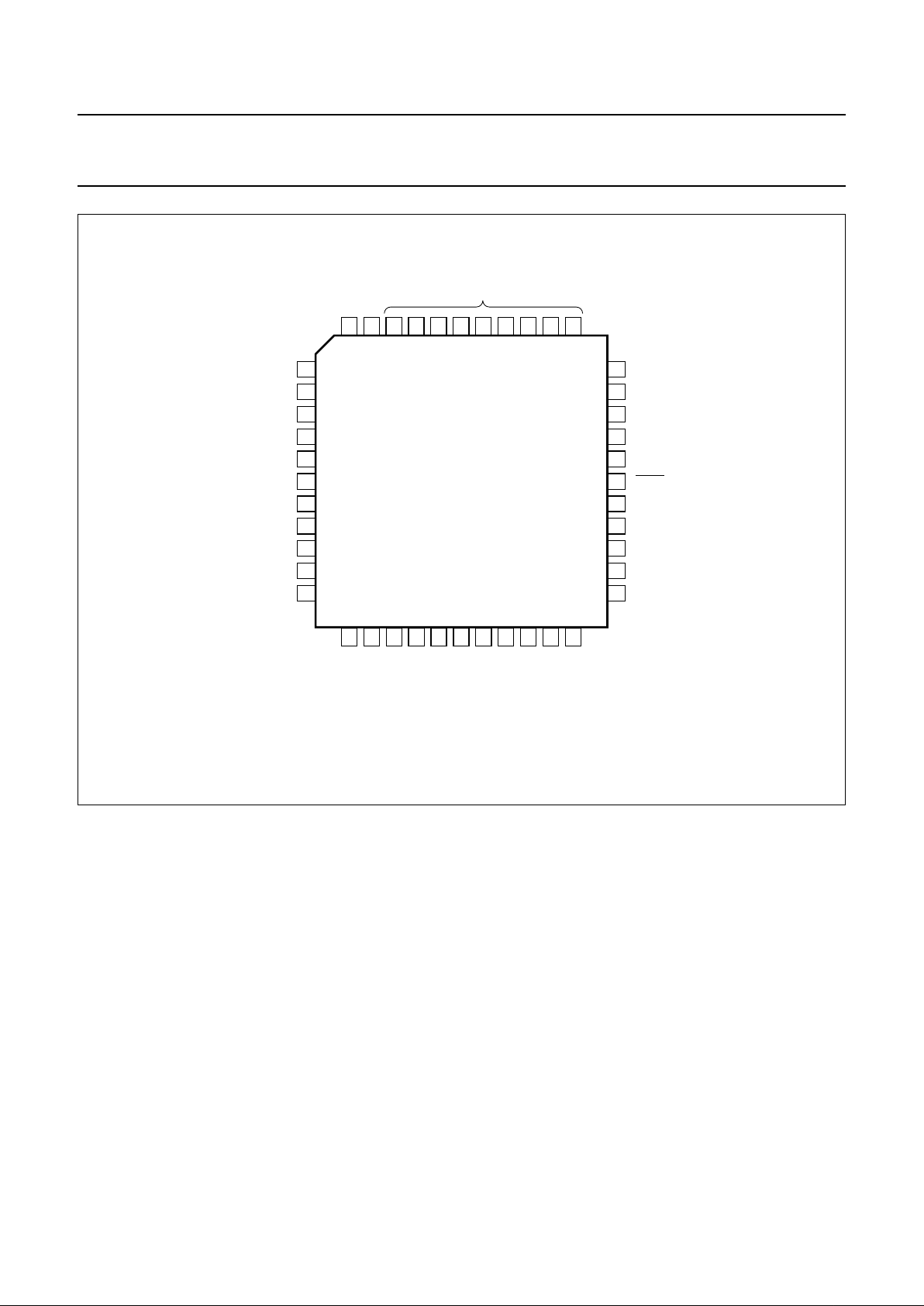
PINNING
Note
1. All supply pins must be connected to the same external power supply.
SYMBOL PIN DESCRIPTION
CL11 1 11.2896 or 5.6448 MHz clock output (3-state); (divide-by-3)
DOBM 2 bi-phase mark output (externally buffered; 3-state)
V1 3 versatile input pin
V2 4 versatile input pin
TEST2 5 test input; this pin should be tied LOW
TEST1 6 test input; this pin should be tied LOW
ISLICE 7 current feedback output from data slicer
HFIN 8 comparator signal input
HFREF 9 comparator common-mode input
IREF 10 reference current pin (nominally
1
⁄2VDD)
V
DDA
11 analog supply voltage; note 1
V
SSA
12 analog ground; note 1
CRIN 13 crystal/resonator input
CROUT 14 crystal/resonator output
V
DD1
15 digital supply to input and output buffers; note 1
V
SS1
16 digital ground to input and output buffers; note 1
CL16 17 16.9344 MHz system clock output
MISC 18 general purpose DAC output (3-state)
DATA 19 serial data output (3-state)
WCLK 20 word clock output (3-state)
SCLK 21 serial bit clock output (3-state)
MOTO1 22 motor output 1; versatile (3-state)
MOTO2 23 motor output 2; versatile (3-state)
V5 24 versatile output pin
V4 25 versatile output pin
V3 26 versatile output pin (open-drain)
KILL 27 kill output; programmable (open-drain)
PORE 28 power-on reset enable input (active LOW)
CLA 29 4.2336 MHz microcontroller clock output
DA 30 interface data I/O line
CL 31 interface clock input line
RAB 32 interface R/
W and acknowledge input
CFLG 33 correction flag output (open-drain)
n.c. 34 to 42 no internal connection
V
SS2
43 digital ground to internal logic; note 1
V
DD2
44 digital supply voltage to internal logic; note 1
1998 Feb 16 5
Philips Semiconductors Product specification
CMOS digital decoding IC with RAM for
Compact Disc
SAA7345
Fig.2 Pin configuration.
MGA359 - 1
1
2
3
4
5
6
7
8
9
10
11
33
32
31
30
29
28
27
26
25
24
23
12
13
14
15
16
17
18
19
20
21
22
44
43
42
41
40
39
38
37
36
35
34
CFLG
RAB
CL
DA
CLA
PORE
KILL
V3
V4
V5
MOTO2
CL11
IREF
DOBM
V1
V2
TEST2
TEST1
ISLICE
HFIN
HFREF
V
DDA
SAA7345
MOTO1
CRIN
CROUT
V
DD1
V
SS1
CL16
MISC
DATA
SCLK
WCLK
V
SSA
V
DD2
V
SS2
Pins 34 to 42 (inclusive)
have no internal connection
1998 Feb 16 6
Philips Semiconductors Product specification
CMOS digital decoding IC with RAM for
Compact Disc
SAA7345
FUNCTIONAL DESCRIPTION
Demodulator
F
RAME SYNC PROTECTION
This circuit will detect the frame synchronization signals.
Two synchronization counters are used in the SAA7345:
1. The coincidence counter which is used to detect the
coincidence of successive syncs. It generates a Sync
coincidence signal if 2 syncs are 588 ±1 EFM clocks
apart.
2. The main counter is used to partition the EFM signal
into 17-bit words. This counter is reset when:
a) A Sync coincidence is generated.
b) A sync is found within ±6 EFM clocks of its
expected position.
The Sync coincidence signal is also used to generate the
Lock signal which will go active HIGH when 1 Sync
coincidence is found. It will reset to LOW when, during 61
consecutive frames, no Sync coincidence is found. This
Lock signal is accessed via the status signal when the
status control register (address 0010) is set to X100. See
section on “Microcontroller interface” .
Data Slicer and Clock Regenerator
The SAA7345 has an integrated slice level comparator
which is clocked by the crystal frequency clock. The slice
level is controlled by an internal current source applied to
an external capacitor under the control of the digital
phase-locked loop (DPLL).
Regeneration of the bit clock is achieved with an internal
fully digital PLL. No external components are required and
the bit clock is not output. The PLL has two microcontroller
control registers (addresses 1000 and 1001) for
bandwidth and equalization.
For certain applications an off-track input is necessary. If
this flag is HIGH, the SAA7345 will assume that the servo
is following on the wrong track, and will flag all incoming
HF data as incorrect. The off-track is input via the V1 pin
when the versatile pins interface register (address 1100)
bit 0 is set to logic 1.
EFM demodulation
The 14-bit EFM data and subcode words are decoded into
8-bit symbols.
Subcode data processing
Q-
CHANNEL PROCESSING
The 96-bit Q-channel word is accumulated in an internal
buffer. Sixteen bits are used to perform a Cyclic
Redundancy Check (CRC). If the data is good, the
SUBQREADY-I signal will go LOW. SUBQREADY-I can
be read via the status signal when the status control
register (address 0010) is set to X000 (normal reset
condition). Good Q-channel data may be read via the
microcontroller interface.
Fig.3 Data slicer showing typical application components.
47 pF
22 nF
2.2 kΩ
HFIN
HFREF
I
ref
ISLICE
22 kΩ
100 nF
2.2 nF
HF
input
crystal
clock
DQ
DPLL
1/2V
DD
V
SSA
V
SS
V
SSA
MGA368 - 1
V
DD
100 µA
100 µA
1998 Feb 16 7
Philips Semiconductors Product specification
CMOS digital decoding IC with RAM for
Compact Disc
SAA7345
OTHER SUBCODE CHANNELS
Data of the other subcode channels (Q-to-W) may be read
via the V4 pin if the versatile pins interface register
(address 1101) is set to XX01.
The format is similar to RS232. The subcode sync word is
formed by a pause of 200 µs minimum. Each subcode byte
starts with a logic 1 followed by 7 bits (Q-to-W). The gap
between bytes is variable between 11.3 µs and 90 µs.
The subcode data is also available in the EBU output
(DOBM) in a similar format.
Microcontroller interface
The SAA7345 has a 3-line microcontroller interface which
is compatible with the digital servo IC TDA1301.
W
RITING DATA TO SAA7345
The SAA7345 has thirteen 4-bit programmable
configuration registers as shown in Table 2. These can be
written to via the microcontroller interface using the
protocol shown in Fig.5.
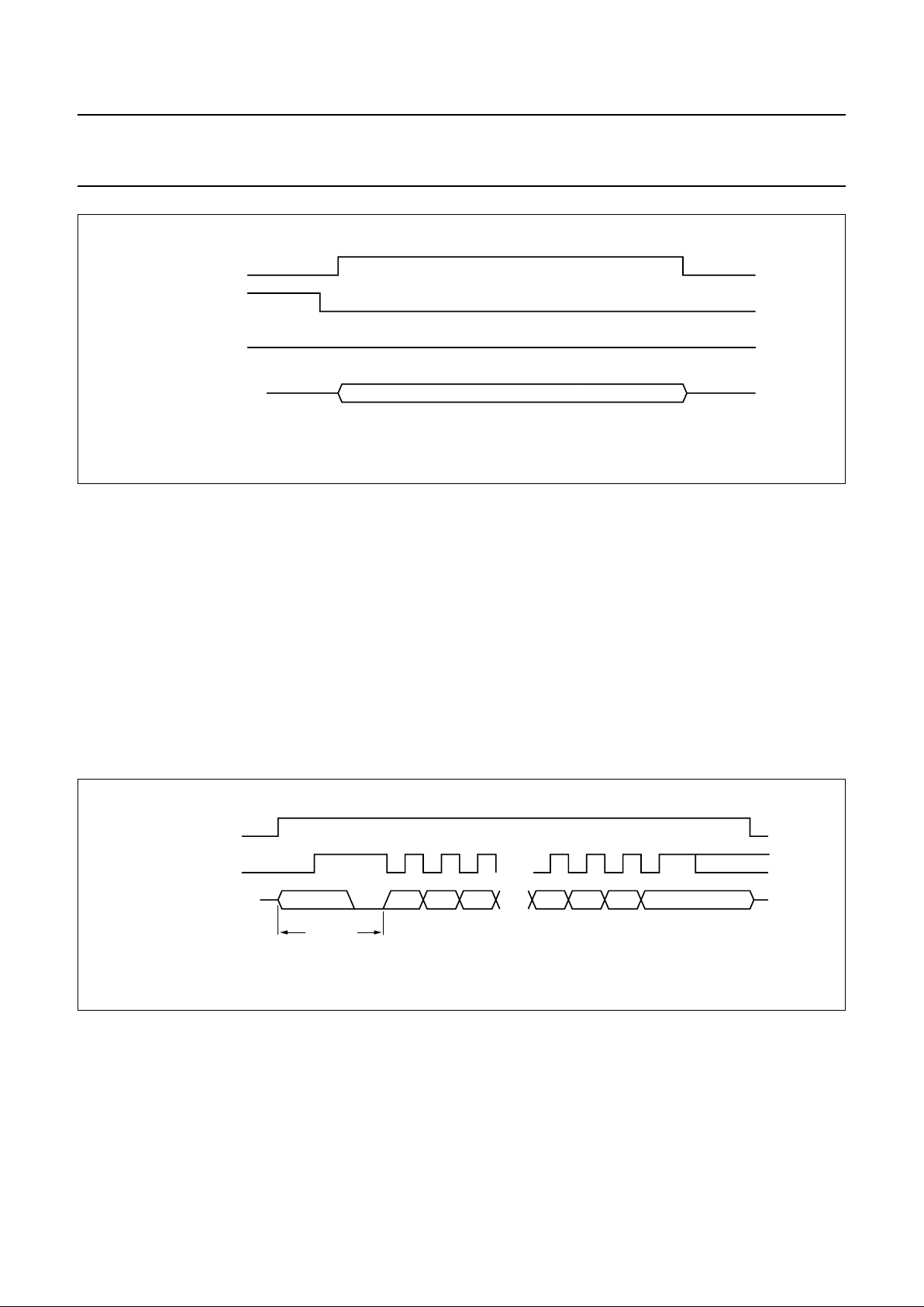
Write operation sequence
• RAB is held LOW by the microcontroller to hold the
SAA7345 DA pin at high-impedance.
• Microcontroller data is clocked into the internal shift
register on the LOW-to-HIGH clock transition CL.
• Data D (3 : 0) is latched into the appropriate control
register [address bits A (3 : 0)] on the LOW-to-HIGH
transition of RAB with CL HIGH.
• If more data is clocked into SAA7345 before the
LOW-to-HIGH transition of RAB then only the last 8 bits
are used.
• If less data is clocked into SAA7345, unpredictable
operation will result.
• If the LOW-to-HIGH transition of RAB occurs with CL
LOW, the command will be disregarded.
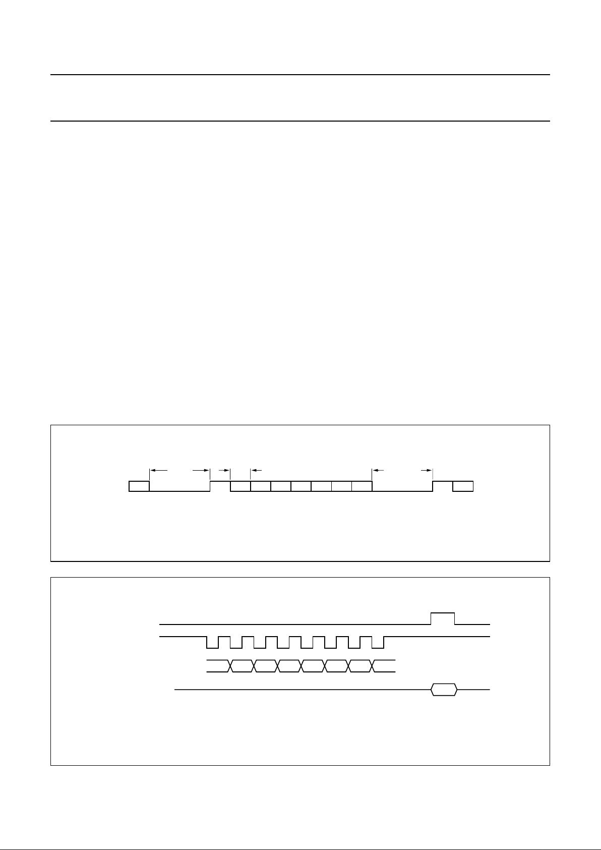
Fig.4 Subcode format and timing at V4 pin.
W96 1 Q1 R1 S1 T1 U1 V1 W1 1 Q2
200 µs
min
11.3
µs
11.3 µs min
90 µs max
MGA369
Fig.5 Microcontroller WRITE timing.
A3 A2 A1 A0 D3 D2 D1 D0
DA (SAA7345)
CL
(microcontroller)
RAB
(microcontroller)
DA
(microcontroller)
MGA379 - 1
high impedance

1998 Feb 16 8
Philips Semiconductors Product specification
CMOS digital decoding IC with RAM for
Compact Disc
SAA7345
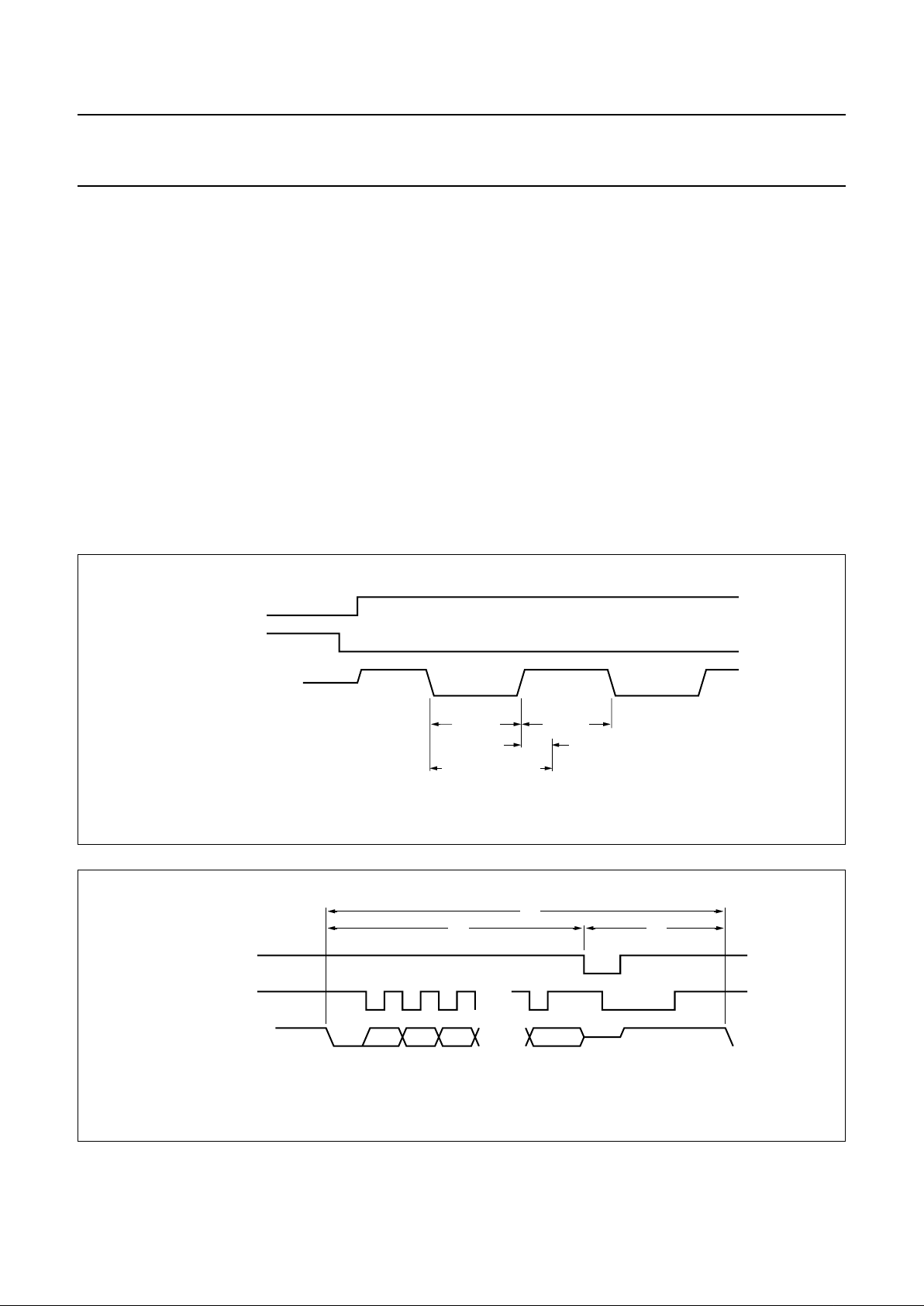
WRITING DATA TO SAA7345; REPEAT MODE
The same command can be repeated several times (e.g. for fade function) by applying extra RAB pulses as shown in
Fig.6.
R
EADING STATUS INFORMATION FROM SAA7345
There are several internal status signals which can be made available on the DA line (Table 1).
Table 1 Internal status signals.
The status signal to be output is selected by status control register (address 0010). The timing for reading the status
signal is shown in Fig.7.
Status read operation sequence
• Write appropriate data to register 0010 to select required status signal.
• With RAB LOW; set CL LOW.
• Set RAB HIGH; this will instruct the SAA7345 to output status signal on DA.
SIGNAL DESCRIPTION
SUBQREADY-I LOW if new subcode word is ready in Q-channel register.
MOTSTART1 HIGH if motor is turning at 75% or more of nominal speed.
MOTSTART2 HIGH if motor is turning at 50% or more of nominal speed.
MOTSTOP HIGH if motor is turning at 12% or less of nominal speed.
PLL Lock HIGH if Sync coincidence signals are found.
V1 Follows input on V1 pin.
V2 Follows input on V2 pin.
MOTOR-OV HIGH if the motor servo output stage saturates.
Note that CL must stay HIGH between RAB pulses.
Fig.6 Microcontroller WRITE timing; repeat mode.
A3 A2 A1 A0 D3 D2 D1 D0
DA (SAA7345)
MGA380 - 1
CL
(microcontroller)
RAB
(microcontroller)
DA
(microcontroller)
high impedance
1998 Feb 16 9
Philips Semiconductors Product specification
CMOS digital decoding IC with RAM for
Compact Disc
SAA7345
READING Q-CHANNEL SUBCODE FROM SAA7345
To read Q-channel subcode from SAA7345, the SUBQREADY-I signal should be selected as status signal. The subcode
read timing is shown in Fig.8.
Read subcode operation sequence
• Monitor SUBQREADY-I status signal.
• When this signal is LOW, and up to 2.3 ms after its LOW-to-HIGH transition, it is permitted to read subcode.
• Set CL LOW, SAA7345 will output first subcode bit (Q1).
• After subcode read starts, the microcontroller may take as long as it wants to terminate read operation.
• SAA7345 will output consecutive subcode bits after each HIGH-to-LOW transition of CL.
• When enough subcode has been read (1 to 96 bits), stop reading by pulling RAB LOW.
P
EAK DETECTOR OUTPUT
In place of the CRC-bits (bits 81 to 96), the peak detector information is added to the Q-channel data. The peak
information corresponds to the highest audio level (absolute value) and is measured on positive peaks. Only the most
significant 8 bits of the peak level are given, in unsigned notation. Bits 81 to 88 contain the LEFT peak value
(bit 88 = MSB) and bits 89 to 96 contain the RIGHT channel (bit 96 = MSB). Value is reset after reading Q-channel data.
Fig.7 SAA7345 status READ timing.
DA (SAA7345)
MGA381 - 1
STATUS
CL
(microcontroller)
RAB
(microcontroller)
DA
(microcontroller)
high impedance
Fig.8 SAA7345 Q-channel subcode READ timing.
Q1 Q2 Q3 Qn–1DA (SAA7345)
MGA382 - 1
Qn–2 Qn
STATUS
CRC
OK
CL
(microcontroller)
RAB
(microcontroller)
1998 Feb 16 10
Philips Semiconductors Product specification
CMOS digital decoding IC with RAM for
Compact Disc
SAA7345
BEHAVIOUR OF THE SUBQREADY-I SIGNAL
When the CRC of the Q-channel word is good, and no
subcode is being read, the SUBQREADY-I signal will react
as shown in Fig.9.
When the CRC is good and subcode is being read, the
timing in Fig.10 applies.
If t1 (SUBQREADY-I LOW to end of subcode read) is
below 2.6 ms, then t2= 13.1 ms (i.e. the microcontroller
can read all subcode frames if it completes the read
operation within 2.6 ms after subcode ready).
If this criterion is not met, it is only possible to guarantee
that t
3
will be below 26.2 ms (approximately).
If subcode frames with failed CRCs are present, the t2 and
t3 times will be increased by 13.1 ms for each defective
subcode frame.
S
HARING THE MICROCONTROLLER INTERFACE
When the RAB pin is held LOW by the microcontroller, it is
permitted to put any signal on the DA and CL lines
(SAA7345 will set output DA to high-impedance). Under
this circumstance these lines may be used for another
purpose (e.g. TDA1301 microcontroller interface Data and
Clock line, see Fig.11).
Fig.9 SUBQREADY-I timing when no subcode is read.
DA (SAA7345)
10.8 ms 15.4 ms
2.3
ms
READ start allowed
high
impedance
CRC OK CRC OK
MGA373 - 1
CL
(microcontroller)
RAB
(microcontroller)
Fig.10 SUBQREADY-I timing when subcode is being read.
Q1 Q2 Q3 QnDA (SAA7345)
t
1
t
2
t
3
MGA374 - 1
CL
(microcontroller)
RAB
(microcontroller)
1998 Feb 16 11
Philips Semiconductors Product specification
CMOS digital decoding IC with RAM for
Compact Disc
SAA7345
Table 2 Command registers.
The ‘INITIAL’ column shows the power-on reset state
REGISTER ADDRESS DATA FUNCTION INITIAL
Fade and Attenuation 0 0 0 0 X 0 0 0 Mute Reset
X 0 1 X Attenuate
X 0 0 1 Full Scale
X 1 0 0 Step Down
X 1 0 1 Step Up
Motor mode 0 0 0 1 X 0 0 0 Motor off mode Reset
X 0 0 1 Motor brake mode 1
X 0 1 0 Motor brake mode 2
X 0 1 1 Motor start mode 1
X 1 0 0 Motor start mode 2
X 1 0 1 Motor jump mode
X 1 1 1 Motor play mode
X 1 1 0 Motor jump mode 1
1 X X X anti-windup active
0 X X X anti-windup off Reset
Status control 0 0 1 0 X 0 0 0 status = SUBQREADY-I Reset
X 0 0 1 status = MOTSTART1
X 0 1 0 status = MOTSTART2
X 0 1 1 status = MOTSTOP
X 1 0 0 status = PLL Lock
X 1 0 1 status = V1
X 1 1 0 status = V2
X 1 1 1 status = MOTOR-OV
0 X X X L channel first at DAC (WCLK normal) Reset
1 X X X R channel first at DAC (WCLK inverted)
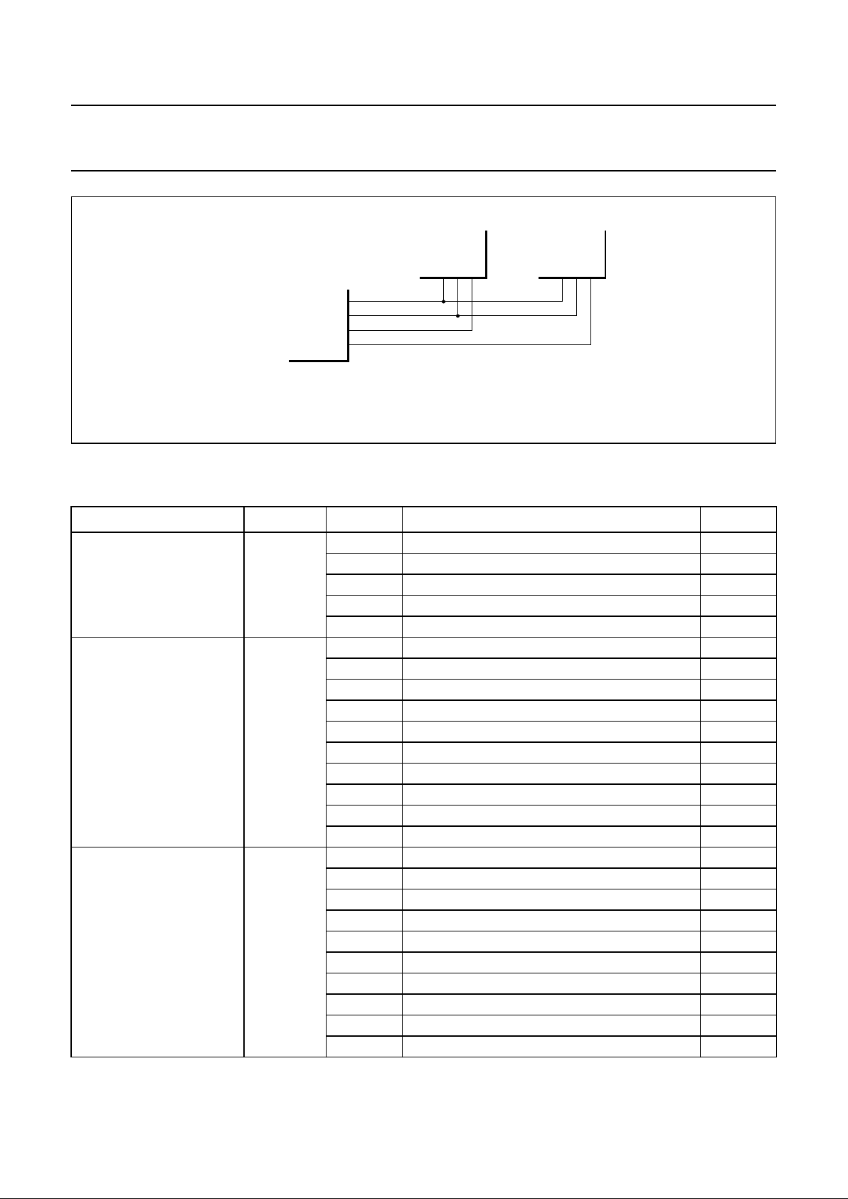
Fig.11 SAA7345 microcontroller interface application diagram.
MGA361 - 1
MICROCONTROLLER
TDA1301 SAA7345
I/O
O
O
O
SIDA
SICL
SILD
DACLRAB

1998 Feb 16 12
Philips Semiconductors Product specification
CMOS digital decoding IC with RAM for
Compact Disc
SAA7345
DAC output 00 1 1 1 0 1 0 I2S CD-ROM mode
1 0 1 1 EIAJ; CD-ROM mode
110 X I
2
S; 4fs mode Reset
1111 I
2
S; 2fs mode
1110 I
2
S; fs mode
0 0 0 X EIAJ; 16-bit; 4f
s
0 0 1 1 EIAJ; 16-bit; 2f
s
0 0 1 0 EIAJ; 16-bit; f
s
0 1 0 X EIAJ; 18-bit; 4f
s
0 1 1 1 EIAJ; 18-bit; 2f
s
0 1 1 0 EIAJ; 18-bit; f
s
Motor gain 0 1 0 0 X 0 0 0 Motor gain G = 3.2 Reset
X 0 0 1 Motor gain G = 4.0
X 0 1 0 Motor gain G = 6.4
X 0 1 1 Motor gain G = 8.0
X 1 0 0 Motor gain G = 12.8
X 1 0 1 Motor gain G = 16.0
X 1 1 0 Motor gain G = 25.6
X 1 1 1 Motor gain G = 32.0
Motor bandwidth 0 1 0 1 X X 0 0 Motor f
4
= 0.5 Hz Reset
X X 0 1 Motor f
4
= 0.7 Hz
X X 1 0 Motor f
4
= 1.4 Hz
X X 1 1 Motor f
4
= 2.8 Hz
0 0 X X Motor f
3
= 0.85 Hz Reset
0 1 X X Motor f
3
= 1.71 Hz
1 0 X X Motor f
3
= 3.42 Hz
Motor output configuration 0 1 1 0 X X 0 0 Motor power maximum 37% Reset
X X 0 1 Motor power maximum 50%
X X 1 0 Motor power maximum 75%
X X 1 1 Motor power maximum 100%
0 0 X X MOTO1, MOTO2 pins 3-state Reset
0 1 X X Motor Pulse Width Modulation (PWM) mode
1 0 X X Motor Pulse Density Modulation (PDM) mode
1 1 X X Motor Compact Disc Video (CDV) mode
REGISTER ADDRESS DATA FUNCTION INITIAL
 Loading...