


DATA SH EET
Product specification
File under Integrated Circuits, IC22
2000 Mar 08
INTEGRATED CIRCUITS
SAA7128H; SAA7129H
Digital video encoder

2000 Mar 08 2
Philips Semiconductors Product specification
Digital video encoder SAA7128H; SAA7129H
CONTENTS
1 FEATURES
2 GENERAL DESCRIPTION
3 ORDERING INFORMATION
4 QUICK REFERENCE DATA
5 BLOCK DIAGRAM
6 PINNING
7 FUNCTIONAL DESCRIPTION
7.1 Versatile fader
7.2 Data manager
7.3 Encoder
7.4 RGB processor
7.5 SECAM processor
7.6 Output interface/DACs
7.7 Synchronization
7.8 Clock
7.9 I2C-bus interface
7.10 Input levels and formats
7.11 Bit allocation map
7.12 I2C-bus format
7.13 Slave receiver
7.14 Slave transmitter
8 CHARACTERISTICS
8.1 Explanation of RTCI data bits
8.2 Teletext timing
9 APPLICATION INFORMATION
9.1 Analog output voltages
10 PACKAGE OUTLINE
11 SOLDERING
11.1 Introduction to soldering surface mount
packages
11.2 Reflow soldering
11.3 Wave soldering
11.4 Manual soldering
11.5 Suitability of surface mount IC packages for
wave and reflow soldering methods
12 DEFINITIONS
13 LIFE SUPPORT APPLICATIONS
14 PURCHASE OF PHILIPS I2C COMPONENTS

2000 Mar 08 3
Philips Semiconductors Product specification
Digital video encoder SAA7128H; SAA7129H
1 FEATURES
• Monolithic CMOS 3.3 V device, 5 V I2C-bus optional
• Digital PAL/NTSC/SECAM encoder
• System pixel frequency 13.5 MHz
• 54 MHz double-speedmultiplexed D1 interface capable
of splitting data into two separate channels (encoded
and baseband)
• Three Digital-to-Analog Converters (DACs) for CVBS
(CSYNC), VBS (CVBS) and C (CVBS) two times
oversampled with 10-bit resolution (signals in brackets
optional)
• Three DACs for RED (CR), GREEN (Y) and BLUE (CB)
two times oversampled with 9-bit resolution (signals in
brackets optional)
• Alternatively, an advanced composite sync is available
on the CVBS output for RGB display centring
• Real-time control of subcarrier
• Cross-colour reduction filter
• Closed captioning encoding and World Standard
Teletext (WST) and North-American Broadcast Text
System(NABTS) teletextencoding includingsequencer
and filter
• Copy Generation Management System (CGMS)
encoding (CGMS described by standard CPR-1204 of
EIAJ); 20 bits in lines 20/283 (NTSC) can be loaded via
I2C-bus
• Fast I2C-bus control port (400 kHz)
• Line 23 Wide Screen Signalling (WSS) encoding
• Video Programming System (VPS) data encoding in
line 16 (50/625 lines counting)
• Encoder can be master or slave
• Programmable horizontal and vertical input
synchronization phase
• Programmable horizontal sync output phase
• Internal Colour Bar Generator (CBG)
• Macrovision Pay-per-View copy protection system
rev. 7.01 and rev. 6.1 as option; this applies to
SAA7128H only. The deviceis protectedby USA patent
numbers 4631603, 4577216 and 4819098 and other
intellectual property rights. Use of the macrovision
anti-copy process in the device is licensed for
non-commercialhome use only. Reverseengineeringor
disassembly is prohibited. Please contact your nearest
PhilipsSemiconductors salesoffice formore information
• Controlled rise/fall times of output syncs and blanking
• On-chip crystal oscillator (3rd-harmonic or fundamental
crystal)
• Downmode (lowoutput voltage) orpower-save modeof
DACs
• QFP44 package.
2 GENERAL DESCRIPTION
The SAA7128H; SAA7129H encodes digital CB-Y-C
R
video data to an NTSC, PAL or SECAM CVBS or S-video
signal. Simultaneously, RGB orbypassed butinterpolated
CB-Y-CR signals are available via three additional DACs.
The circuit at a 54 MHz multiplexed digital D1 input port
accepts two ITU-R BT.656 compatible CB-Y-CR data
streams with 720 active pixels per line in
4:2:2multiplexed formats, for example MPEG decoded
data with overlay and MPEG decoded data without
overlay, whereas one data stream is latched at the rising,
the other one at the falling clock edge.
It includes a sync/clock generator and on-chip DACs.
3 ORDERING INFORMATION
TYPE NUMBER
PACKAGE
NAME DESCRIPTION VERSION
SAA7128H QFP44 plastic quad flat package; 44 leads (lead length 1.3 mm); body
10 × 10 × 1.75 mm
SOT307-2
SAA7129H

2000 Mar 08 4
Philips Semiconductors Product specification
Digital video encoder SAA7128H; SAA7129H
4 QUICK REFERENCE DATA
SYMBOL PARAMETER MIN. TYP. MAX. UNIT
V
DDA
analog supply voltage 3.15 3.3 3.45 V
V
DDD
digital supply voltage 3.0 3.3 3.6 V
I
DDA
analog supply current − 130 150 mA
I
DDD
digital supply current − 75 100 mA
V
i
input signal voltage levels TTL compatible
V
o(p-p)
analog output signal voltages Y, C and CVBS without load
(peak-to-peak value)
1.25 1.35 1.50 V
R
L
load resistance 75 − 300 Ω
LE
lf(i)
low frequency integral linearity error −−±3 LSB
LE
lf(d)
low frequency differential linearity error −−±1 LSB
T
amb
ambient temperature 0 − 70 °C
2000 Mar 08 5
Philips Semiconductors Product specification
Digital video encoder SAA7128H; SAA7129H
This text is here in white to force landscape pages to be rotated correctly when browsing through the pdf in the Acrobat reader.This text is here in
_white to force landscape pages to be rotated correctly when browsing through the pdf in the Acrobat reader.This text is here inThis text is here in
white to force landscape pages to be rotated correctlywhenbrowsing through the pdf in the Acrobat reader. white to forcelandscapepages to be ...
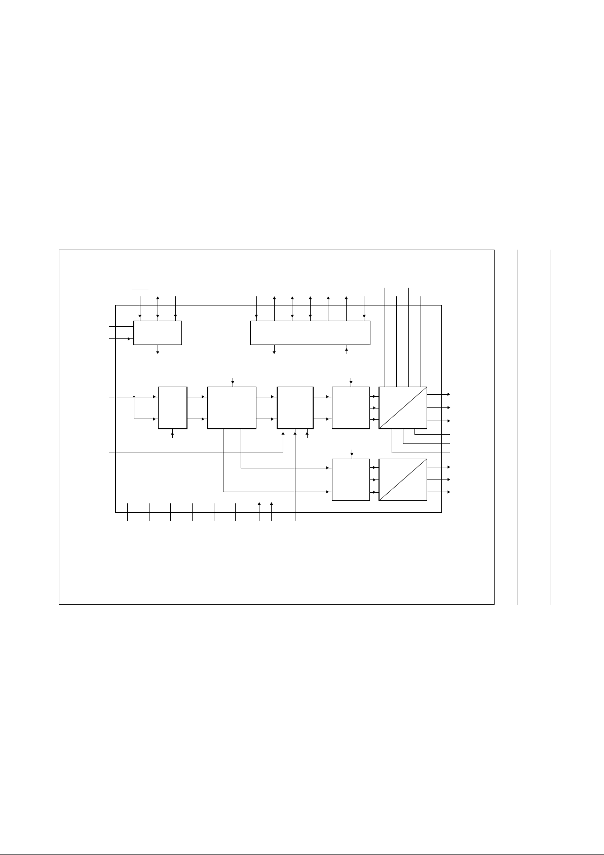
5 BLOCK DIAGRAM
f
ull pagewidth
MHB572
I2C-BUS
INTERFACE
SYNC/CLOCK
I
2
C-bus control
21
41
SCL
V
DDA4
42
SDA
40
SA
9 to 16
MP7 to MP0
44
TTX
20
V
DD(I2C)
D
Y
C
A
36
V
DDA3
31
V
DDA2
28
V
DDA1
25
clock and timing
35
XTALI
I2C-bus control
34
XTALO7RCV18RCV243TTXRQ37XCLK4LLC1
19
RTCI
CVBS
(CSYNC)
30
VBS
(CVBS)
27
C
(CVBS)
24
OUTPUT
INTERFACE
ENCODER
Y
CbCr
FADER
V
SSA1
22
V
SSA2
32
V
SSA3
33
I2C-bus
control
3AP2
SP
39
V
DDD3
17
V
DDD2
6
V
DDD1
38
V
SSD3
18
V
SSD2
5
V
SSD1
MP
A
MP
B
MP
pos
MP
neg
MP
VP
SWITCH
I2C-bus control
I2C-bus controlI2C-bus control
RESET
D
Y
CbCr
A
RED
23
GREEN
26
BLUE
29
RGB
PROCESSOR
I2C-bus control
SAA7128H
SAA7129H
Fig.1 Block diagram.

2000 Mar 08 6
Philips Semiconductors Product specification
Digital video encoder SAA7128H; SAA7129H
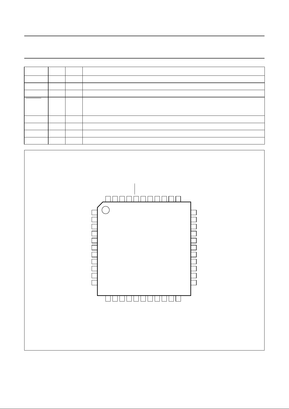
6 PINNING
SYMBOL PIN TYPE DESCRIPTION
RES 1 − reserved pin; do not connect
SP 2 I test pin; connected to digital ground for normal operation
AP 3 I test pin; connected to digital ground for normal operation
LLC1 4 I line-locked clock input; this is the 27 MHz master clock
V
SSD1
5 supply digital ground 1
V
DDD1
6 supply digital supply voltage 1
RCV1 7 I/O raster control 1 for video port; this pin receives/provides a VS/FS/FSEQ signal
RCV2 8 I/O raster control 2 for video port; this pin provides an HS pulse of programmable length or
receives an HS pulse
MP7 9 I double-speed 54 MHz MPEG port; it is an input for
“ITU-R BT.656”
style multiplexed
CB-Y-CR data; data is sampled on the rising and falling clock edge; data sampled on the
rising edge is then sent to the encoding part of the device; data sampled on the falling
edge is sent to the RGB part of the device (or vice versa, depending on programming)
MP6 10 I
MP5 11 I
MP4 12 I
MP3 13 I
MP2 14 I
MP1 15 I
MP0 16 I
V
DDD2
17 supply digital supply voltage 2
V
SSD2
18 supply digital ground 2
RTCI 19 I real-time control input; if the LLC1 clock is provided by an SAA7111 or SAA7151B, RTCI
should be connected to the RTCO pin of the respective decoder to improve the signal
quality
V
DD(I2C)
20 supply sense input for I2C-bus voltage; connect to I2C-bus supply
SA 21 I select I
2
C-bus address; LOW selects slave address 88H, HIGH selects slave address
8CH
V
SSA1
22 supply analog ground 1 for RED (CR), C (CVBS) and GREEN (Y) outputs
RED 23 O analog output of RED (C
R
) signal
C 24 O analog output of chrominance (CVBS) signal
V
DDA1
25 supply analog supply voltage 1 for RED (CR) and C (CVBS) outputs
GREEN 26 O analog output of GREEN (Y) signal
VBS 27 O analog output of VBS (CVBS) signal
V
DDA2
28 supply analog supply voltage 2 for VBS (CVBS) and GREEN (Y) outputs
BLUE 29 O analog output of BLUE (C
B
) signal
CVBS 30 O analog output of CVBS (CSYNC) signal
V
DDA3
31 supply analog supply voltage 3 for BLUE (CB) and CVBS (CSYNC) outputs
V
SSA2
32 supply analog ground 2 for VBS (CVBS), BLUE (CB) and CVBS (CSYNC) outputs
V
SSA3
33 supply analog ground 3 for the DAC reference ladder and the oscillator
XTALO 34 O crystal oscillator output
XTALI 35 I crystal oscillator input; if the oscillator is not used, this pin should be connected to ground
V
DDA4
36 supply analog supply voltage 4 for the DAC reference ladder and the oscillator
2000 Mar 08 7
Philips Semiconductors Product specification
Digital video encoder SAA7128H; SAA7129H
XCLK 37 O clock output of the crystal oscillator
V
SSD3
38 supply digital ground 3
V
DDD3
39 supply digital supply voltage 3
RESET 40 I Reset input, active LOW. After reset is applied, all digital I/Os are in input mode; PAL
black burst on CVBS, VBS and C; RGB outputs set to lowest voltage. The I2C-bus
receiver waits for the START condition.
SCL 41 I I
2
C-bus serial clock input
SDA 42 I/O I
2
C-bus serial data input/output
TTXRQ 43 O teletext request output, indicating when text bits are requested
TTX 44 I teletext bit stream input
SYMBOL PIN TYPE DESCRIPTION
handbook, full pagewidth
1
2
3
4
5
6
7
8
9
10
11
33
32
31
30
29
28
27
26
25
24
23
12
13
14
15
16
17
18
19
20
21
22
44
43
42
41
40
39
38
37
36
35
34
SAA7128H
SAA7129H
MHB573
V
SSA3
V
SSA2
V
DDA3
CVBS
V
DDA2
VBS
GREEN
V
DDA1
C
RED
RES
SP
AP
LLC1
V
SSD1
V
DDD1
RCV2
MP7
MP5
BLUE
TTXRQ
SDA
SCL
V
DDD3
V
SSD3
V
DDA4
XTALI
XTALO
TTX
XCLK
MP3
MP2
MP1
MP0
V
DDD2
V
SSD2
V
DD(I2C)
SA
V
SSA1
MP4
RTCI
RCV1
MP6
RESET
Fig.2 Pin configuration.

2000 Mar 08 8
Philips Semiconductors Product specification
Digital video encoder SAA7128H; SAA7129H
7 FUNCTIONAL DESCRIPTION
The digital video encoder encodes digital luminance and
colour difference signals into analog CVBS, S-video and
simultaneously RGB or CR-Y-CB signals. NTSC-M, PAL
B/G, SECAM and sub-standards are supported.
Both interlaced and non-interlaced operation is possible
for all standards.
The basic encoder function consists of subcarrier
generation and colour modulation and insertion of
synchronization signals. Luminance and chrominance
signals are filtered in accordance with the standard
requirements of
“RS-170-A”
and
“ITU-R BT.470-3”
.
For ease of analog post filtering the signals are twice
oversampled with respect to the pixel clock before
digital-to-analog conversion.
The total filter transfer characteristics are illustrated in
Figs 8 to 13. The DACs for Y, C and CVBS are realized
with full 10-bit resolution; 9-bit resolution for RGB output.
TheCR-Y-CBtoRGB dematrixcan be bypassed optionally
in order to provide the upsampled CR-Y-CB input signals.
The8-bit multiplexed CB-Y-CRformatsare
“ITU-R BT.656”
(D1 format) compatible, but the SAV and EAV codes can
be decoded optionally, when the device is operated in
slave mode. Two independent data streams can be
processed, one latched by the rising edge of LLC1, the
other latched by the falling edge of LLC1. The purpose of
that is e.g. to forward one of the data streams containing
both video and On-Screen Display (OSD) information to
the RGB outputs, and the other stream containing video
only to the encoded outputs CVBS and S-video.
For optimum display of RGB signals through a
euro-connector TV set, optionally on the CVBS output an
early composite sync pulse (up to 31 LLC1 clock periods)
can be provided.
As a further alternative, the VBS and C outputs may
provide a second and third CVBS signal.
Itis alsopossible to connecta Philips digitalvideo decoder
(SAA7111, SAA7711A, SAA7112 or SAA7151B) to the
SAA7128H; SAA7129H. Via the RTCI pin, connected to
RTCO of a decoder, information concerning actual
subcarrier, PAL-ID and (with SAA7111 and newer types)
definite subcarrier phase can be inserted.
The device synthesizes all necessary internal signals,
colour subcarrier frequency, and synchronization signals,
from that clock.
Wide screen signalling data can be loadedvia the I2C-bus
and is inserted into line 23 for standards using 50 Hz field
rate.
VPS data for program dependent automatic startand stop
of such featured VCR’s is loadable via I2C-bus.
The IC also contains closed caption and extended data
services encoding (line 21), and supports anti-taping
signalgeneration in accordancewithmacrovision.It is also
possible to load data for copy generation management
system into line 20 of every field (525/60 line counting).
A number of possibilities are provided for setting different
video parameters such as:
• Black and blanking level control
• Colour subcarrier frequency
• Variable burst amplitude etc.
During reset (RESET = LOW) and after reset is released,
all digital I/O stages are set to input mode and the encoder
is set to PAL mode and outputs a ‘black burst’ signal on
CVBS and S-video outputs, while RGB outputs are set to
their lowest output voltages. A reset forces the I2C-bus
interface to abort any running bus transfer.
7.1 Versatile fader
Important note: whenever the fader is activated with the
SYMP bit set to a logic 1 (enabling the detection of
embedded Start of Active Video (SAV) and End of Active
Video (EAV)), codes 00H and FFH are not allowed within
the actual video data (as prescribed by
“ITU-R BT.
656”,
anyway). If SAV (00H) has been detected, the fader
automatically passes 100% of the respective signal until
SAV will be detected.
Within the digital video encoder, two data streams can be
faded against each other; these data streams can be input
to the double speed MPEG port, which is able to separate
two independent 27 MHz data streams MPA and MPB via
a cross switch controlled by EDGE1 and EDGE2.
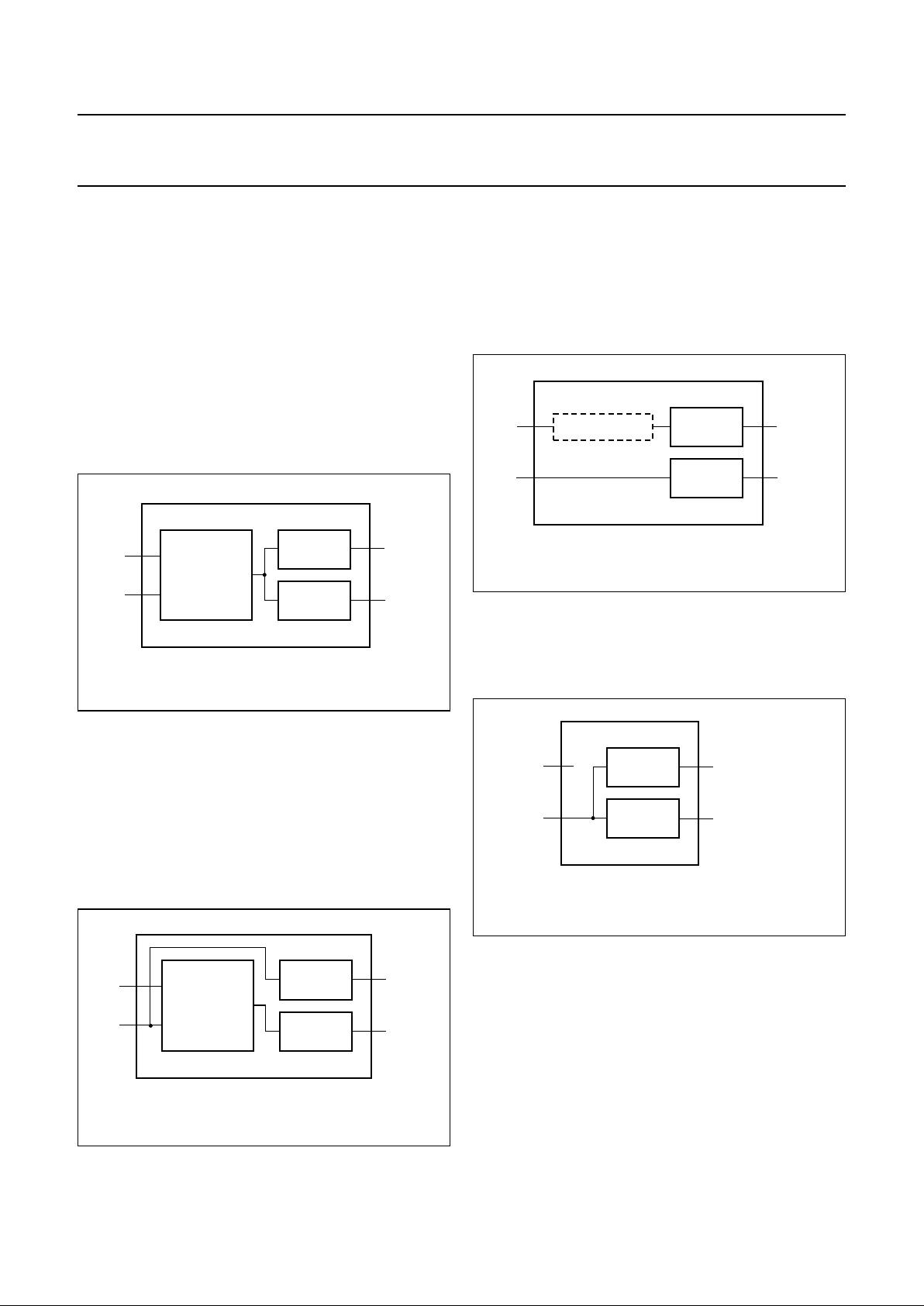
handbook, halfpage
MHB574
MP
A
MP
B
MP
pos
MP
neg
EDGE1 = 0
EDGE1 = 1
EDGE2 = 1
EDGE2 = 0
Fig.3 Cross switch.
2000 Mar 08 9
Philips Semiconductors Product specification
Digital video encoder SAA7128H; SAA7129H
7.1.1 CONFIGURATION EXAMPLES
Figs 4 to 7 show examples on how to configure the fader
between the input ports and the outputs, separated into
the composite (and S-video) encoder and the RGB
encoder.
7.1.1.1 Configuration 1
Input MPAcan be faded into MPB. The resulting output of
the fader is then encoded simultaneously to composite
(and S-video) and RGB output (RGBIN = ENCIN = 1).
In this example, either MPA or MPB could be an overlay
(menu) signal to be faded smoothly in and out.
7.1.1.2 Configuration 2
Input MPAcan be faded into MPB. The resulting output of
the fader is then encoded to RGB output, while the signal
comingfromMPBisfeddirectly to composite(andS-video)
output (RGBIN = 1, ENCIN = 0). Also in this example,
either MPAor MPBcould be anoverlay (menu)signal to be
faded smoothly in and out, whereas the overlay appears
only in the RGB output connected to the TV set.
7.1.1.3 Configuration 3
Input MPBis passeddirectly to the RGB output, assuming
e.g.it contains videoincludingoverlay. MPAisequivalently
passed through the inactive fader to the composite (and
S-video) output,assuming e.g. it contains video excluding
overlay (RGBIN = 0, ENCIN = 1).
7.1.1.4 Configuration 4
OnlyMPBinputis in use;itssignal appears bothcomposite
(and S-video) and RGB encoded (RGBIN = ENCIN = 0).
MHB575
ENCODER
PATH
RGB PATH
FADER
OUTPUT
MP
A
MP
B
MP
e.g.
video
recorder
e.g. TV
VP
Fig.4 Configuration 1.
MHB576
ENCODER
PATH
RGB PATH
FADER
OUTPUT
MP
A
MP
B
MP
e.g. TV
VP
e.g.
video
recorder
Fig.5 Configuration 2.
MHB577
ENCODER
PATH
RGB PATH
FADER BYPASS
MP
A
MP
B
e.g. TV
e.g.
video
recorder
Fig.6 Configuration 3.
handbook, halfpage
MHB578
ENCODER
PATH
RGB PATH
MP
A
MP
B
e.g. video recorder
e.g. TV
Fig.7 Configuration 4.

2000 Mar 08 10
Philips Semiconductors Product specification
Digital video encoder SAA7128H; SAA7129H
7.1.2 PARAMETERS OF THE FADER
Basically, there are three independent fade factors
available, allowing for the equation:
Where x = 1, 2 or 3
Factor FADE1 is effective, when a colour in the data
stream fed to the MPEG port fader input is recognized as
being between KEY1L and KEY1U. That means, the
colour is not identified by a single numeric value, but an
upper and lower threshold in a 24-bit YUV colour space
canbe defined. FADE1 = 00Hresultsin100% signal atthe
MPEG port fader input and 0% signal at the fader Video
port input. Variation of 63 steps is possible up to
FADE1 = 3FH, resulting in 0% signal at the MPEG port
fader input and 100% signal at the fader Video port input.
Factor FADE2 is effective, when a colour in the data
stream fed to the MPEG port fader input is recognized as
being between KEY2L and KEY2U. FADE2 is to be seen
in conjunction with a colour that is defined by a 24-bit
internal Colour Look-Up Table (CLUT). FADE2 = 00H
results in 100% of the internally defined LUT colour and
0% signal at the fader Video port input. Variation of
63 stepsis possibleupto FADE2 = 3FH,resulting in0%of
the internally defined LUT colour and 100% signal at the
fader Video port input.
Finally,factor FADE3 iseffective,whena colour inthedata
stream fed to the MPEG port fader input is recognized as
neither being between KEY1L and KEY1U nor being
between KEY2L and KEY2H. FADE3 = 00H results in
100% signal at the MPEG port fader input and 0% signal
at the fader Video port input. Variation of 63 steps is
possible up to FADE3 = 3FH, resulting in 0% signal at the
MPEG port fader input and 100%signal atthe fader Video
port input.
Optionally, all upper and lower thresholds can be ignored,
enabling to fade signals only against the LUT colour.
If bit CFADM is set HIGH, all data at the MPEG port fader
are faded against the LUT colour, if bit CFADV is set
HIGH,all dataatthe Videoportfader arefadedagainst the
LUT colour.
7.2 Data manager
In the data manager, alternatively to the external video
data, a pre-defined colour look-up table located in this
block can be read out in a pre-defined sequence (8 steps
per active video line), achieving a colour bar test pattern
generator without the need for an external data source.
7.3 Encoder
7.3.1 VIDEO PATH
The encoder generates out of Y, U and V baseband
signals luminance and colour subcarrier output signals,
suitable for use as CVBS or separate Y and C signals.
Luminance is modified in gain and in offset (latter
programmable in a certain range to enable different black
level set-ups). After insertion of a fixed synchronization
pulse tip level, in accordance with standard composite
synchronization schemes, a blanking level can be set.
Other manipulations used for the macrovision anti-taping
process like additional insertion of AGC super-white
pulses (programmable in height) are supported by
SAA7128H only.
In order to enable easy analog post filtering, luminance is
interpolated from 13.5 MHz data rate to 27 MHzdata rate,
providing luminance in 10-bit resolution. The transfer
characteristics of the luminance interpolation filter are
illustrated in Figs 10 and 11. Appropriate transients at
start/end of active video and for synchronization pulses
are ensured.
Chrominance is modified in gain (programmable
separately for U and V), standard dependent burst is
inserted, before baseband colour signals are interpolated
from 6.75 MHz data rate to 27 MHz data rate. One of the
interpolation stages can be bypassed, thus providing a
higher colour bandwidth, which can be made use of for
Y and C output. The transfer characteristics of the
chrominance interpolation filter are illustrated in
Figs 8 and 9.
Theamplitude, beginningand ending ofthe insertedburst,
is programmable in a certain range that is suitable for
standard signals and for special effects. Behind the
succeeding quadrature modulator, colour in 10-bit
resolution is provided on subcarrier.
The numeric ratio between Y and C outputs is in
accordance with the respective standards.
Output FADEx ln1×()1 FADEx–()ln2×[]+=

2000 Mar 08 11
Philips Semiconductors Product specification
Digital video encoder SAA7128H; SAA7129H
7.3.2 TELETEXT INSERTION AND ENCODING
Pin TTX receives a WST or NABTS teletext bitstream
sampled at the LLC clock. Two protocols are provided:
• At each rising edge of output signal (TTXRQ) a single
teletext bit has to be provided after a programmable
delay at input pin TTX
• Thesignal TTXRQ performsonlya single LOW-to-HIGH
transition and remains atHIGH levelfor 360,296 or 288
teletext bits, depending on the chosen standard.
Phase variant interpolationis achievedon thisbitstream in
the internal teletext encoder, providing sufficient small
phase jitter on the output text lines.
TTXRQ provides a fully programmable request signal to
the teletext source, indicating the insertion period of
bitstream at lines which are selectable independently for
both fields. The internal insertion window for text is set to
360 (PAL-WST), 296 (NTSC-WST) or 288 (NABTS)
teletext bits including clock run-in bits. The protocol and
timing are illustrated in Fig.23.
7.3.3 VIDEO PROGRAMMING SYSTEM (VPS) ENCODING
Five bytes of VPS information can be loaded via the
I2C-bus and will be encoded in the appropriate format into
line 16.
7.3.4 CLOSED CAPTION ENCODER
Using this circuit,data inaccordance withthe specification
of closed caption or extended data service, delivered by
the control interface, can be encoded (line 21). Two
dedicated pairs of bytes (two bytes per field), each pair
preceded by run-in clocks and framing code, are possible.
Theactual line numberwheredata is tobeencoded in, can
be modified in a certain range.
The data clock frequency is in accordance with the
definition for NTSC-M standard 32 times horizontal line
frequency.
DataLOW at theoutputof the DACscorresponds to 0 IRE,
data HIGH at the output of the DACs corresponds to
approximately 50 IRE.
It is also possible to encode closed caption data for 50 Hz
field frequencies at 32 times horizontal line frequency.
7.3.5 ANTI-TAPING (SAA7128H ONLY)
For more information contact your nearest Philips
Semiconductors sales office.
7.4 RGB processor
This block contains a dematrix in order to produce red,
green and blue signals to be fed to a SCART plug.
Before Y, CBand CR signals are de-matrixed, individual
gain adjustment for Y and colour difference signals and
2 times oversampling for luminance and 4 times
oversampling for colour difference signals is performed.
The transfer curves of luminance and colour difference
components of RGB are illustrated in Figs 12 and 13.
7.5 SECAM processor
SECAM specific pre-processing is achieved in this block
by a pre-emphasis of colour difference signals (for gain
and phase see Figs 14 and 15).
A baseband frequency modulator with a reference
frequency shifted from 4.286 MHz to DC carries out
SECAM modulation in accordance with appropriate
standard or optionally wide clipping limits.
Afterthe HF pre-emphasis,alsoapplied on aDCreference
carrier (anti-Clochefilter; see Figs 16 and 17),line-by-line
sequential carriers with black reference of 4.25 MHz (Db)
and 4.40625 MHz (Dr) are generated using specified
values for FSC programming bytes.
Alternating phase reset in accordance with SECAM
standard is carried out automatically. During vertical
blanking the so-called bottle pulses are not provided.
7.6 Output interface/DACs
In the output interface, encoded Y and C signals are
converted from digital-to-analog in a 10-bit resolution.
Y and C signals are also combined to a 10-bit CVBS
signal.
The CVBS output occurs with the same processing delay
(equal to 82 LLC clock periods, measured from MP input
to the analog outputs) as the Y, C and RGB outputs.
Absolute amplitude at the input of the DAC for CVBS is
reduced by15⁄16 with respect to Y and C DACs to make
maximum use of conversion ranges.
Red, green and blue signals are also converted from
digital-to-analog, each providing a 9-bit resolution.
Outputs of the DACs can be set together via software
control to minimum output voltage (approximately 0.2 V
DC) for either purpose. Alternatively, the buffers can be
switchedinto 3-state outputcondition;this allowsfor‘wired
AND’ing with other 3-state outputs and can also be used
as a power-save mode.

2000 Mar 08 12
Philips Semiconductors Product specification
Digital video encoder SAA7128H; SAA7129H
7.7 Synchronization
The synchronization of theSAA7128H; SAA7129His able
to operate in two modes; slave mode and master mode.
In master mode (see Fig.19), the circuit generates all
necessary timings in the video signal itself, and it can
provide timing signals at the RCV1 and RCV2 ports.
In slavemode, itacceptstiming informationeitherfrom the
RCV pins or from the embedded timing data of the
ITU-R BT.656 data stream.
For the SAA7128H; SAA7129H, the only difference
between master and slave mode is that it ignores the
timing information at its inputs in master mode. Thus, if in
slave mode, any timing information is missing, the IC will
continue running free without a visible effect. But there
must not be any additional pulses (with wrong phase)
because the circuit will not ignore them.
In slave mode (see Fig.18), an interface circuit decides,
which signal is expected at the RCV1 port and which
information is taken from its active slope. The polarity can
be chosen, if PRCV1 is logic 0 the rising slope will be
active.
The signal can be:
• A Vertical Sync (VS) pulse; the active slope sets the
vertical phase
• An odd/even signal; the active slope sets the vertical
phase, the internal field flag to odd and optionally sets
the horizontal phase
• A Field Sequence (FSEQ) signal; it marks the first field
of the 4 (NTSC), 8 (PAL) respectively 12 (SECAM) field
sequence. In additionto theodd/even signal,it also sets
the PAL phase and optionally defines the subcarrier
phase.
On the RCV2 port, the IC can provide a horizontal pulse
withprogrammable startand stop phase;this pulsecan be
inhibited in the vertical blanking period to build up, for
example, a composite blanking signal.
The horizontal phase can be set via a separate input
RCV2. In the event of VS pulses at RCV1, this is
mandatory.It is alsopossible to setthesignal path toblank
via this input.
From the ITU-R BT.656 data stream, the SAA7128H;
SAA7129Hdecodes only thestart of thefirstline in theodd
field. All other information is ignored and may miss. If this
kind of slave mode is active, the RCV pins may be
switched to output mode.
In slave mode, the horizontal trigger phase can be
programmed to any point in the line, the vertical phase
from line 0 to line 15 counted from the first serration pulse
in half line steps.
Whenever synchronization information cannot be derived
directly from the inputs, the SAA7128H; SAA7129H will
calculate it from the internal horizontal, vertical and PAL
phase. This gives good flexibility with respect to external
synchronization but the circuit does not suppress illegal
settings. In such an event, e.g the odd/even information
may vanish as it does in the non-interlaced modes.
In master mode, the line lengths are fixed to 1728 clocks
at 50 Hz and 1716 clocks at 60 Hz. To allow
non-interlaced frames, the field lengths can be varied by
±0.5 lines. In the event of non-interlace, the SAA7128H;
SAA7129Hdoes not provideodd/even information andthe
output signal does not contain the PAL ‘Bruch sequence’.
At the RCV1 pin the IC can provide:
• A Vertical Sync(VS) signalwith 2.5 (50 Hz)or 3 (60 Hz)
lines duration
• An odd/even signal which is LOW in odd fields
• A Field Sequence (FSEQ) signal which is HIGH in the
first field of the 4, 8 respectively 12 field sequence.
At the RCV2 pin, there is a horizontal pulse of
programmable phase and duration available. This pulse
can be suppressed in the programmable inactive part of a
field giving a composite blank signal.
The directions and polarities of the RCV ports can be
chosen independently. Timing references can be found in
Tables 52 and 60.
7.8 Clock
The input to LLC1 can either be an external clock source
or the buffered on-chip clock XCLK. The internal crystal
oscillator can be run with either a 3rd-harmonic or a
fundamental crystal.
7.9 I
2
C-bus interface
The I2C-bus interface is a standard slave transceiver,
supporting 7-bit slave addresses and 400 kbits/s
guaranteed transfer rate. It uses 8-bit subaddressing with
an auto-increment function. All registers are write and
readable, except one read only status byte.
The I2C-bus slave address is defined as 88H with pin 21
(SA) tied LOW and as 8CH with pin 21 (SA) tied HIGH.
2000 Mar 08 13
Philips Semiconductors Product specification
Digital video encoder SAA7128H; SAA7129H
7.10 Input levels and formats
TheSAA7128H; SAA7129H expectsdigitalY, CB,CRdata
with levels (digital codes) in accordance with
“ITU-R BT.601”
.
For C and CVBS outputs, deviating amplitudes of the
colour difference signals can be compensated by
independent gain control setting, while gain for luminance
is set to predefined values, distinguishable for 7.5 IRE
set-up or without set-up.
The RGB, respectively CR-Y-CB path features a gain
setting individually for luminance (GY) and colour
difference signals (GCD).
Reference levels are measured with a colour bar,
100% white, 100% amplitude and 100% saturation.
Table 1
“ITU-R BT.601”
signal component levels
Notes
1. Transformation:
a) R = Y + 1.3707 × (CR− 128)
b) G = Y − 0.3365 × (CB− 128) − 0.6982 × (CR− 128)
c) B = Y + 1.7324 × (CB− 128).
2. Representation of R, G and B (or CR, Y and CB) at the output is 9 bits at 27 MHz.
Table 2 8-bit multiplexed format (similar to
“ITU-R BT.601”
)
COLOUR
SIGNALS
(1)
YC
B
C
R
R
(2)
G
(2)
B
(2)
White 235 128 128 235 235 235
Yellow 210 16 146 235 235 16
Cyan 170 166 16 16 235 235
Green 145 54 34 16 235 16
Magenta 106 202 222 235 16 235
Red 81 90 240 235 16 16
Blue 41 240 110 16 16 235
Black 16 128 128 16 16 16
TIME
BITS
01234567
Sample C
B
0Y0C
R
0Y1C
B
2Y2C
R
2Y3
Luminance pixel number 0123
Colour pixel number 0 2

2000 Mar 08 14
Philips Semiconductors Product specification
Digital video encoder SAA7128H; SAA7129H
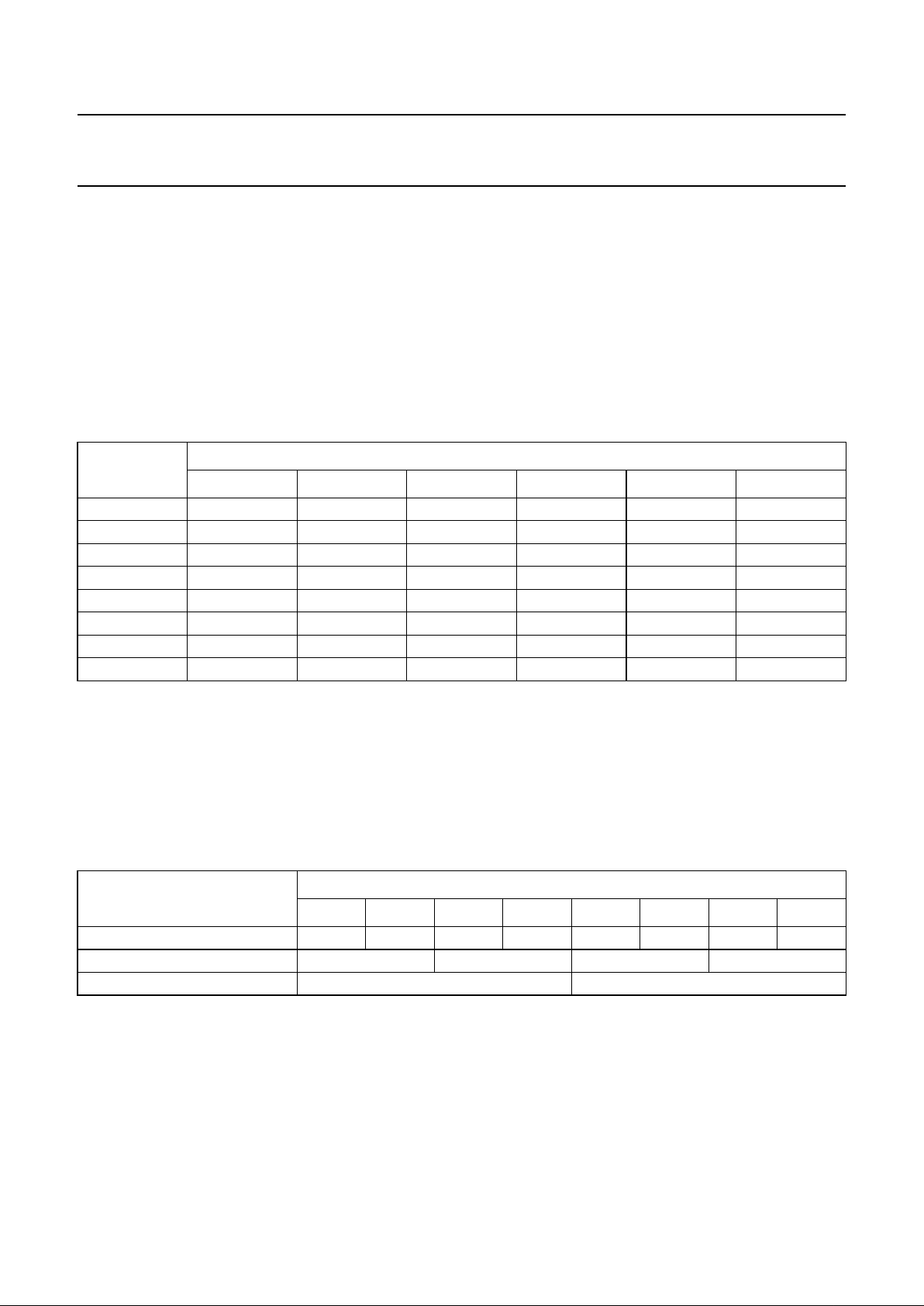
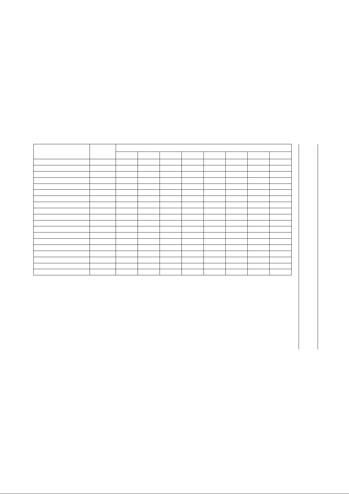
7.11 Bit allocation map
Table 3 Slave receiver (slave address 88H)
REGISTER FUNCTION SUBADDR
DATA BYTE
(1)
D7 D6 D5 D4 D3 D2 D1 D0
Status byte (read only) 00H VER2 VER1 VER0 CCRDO CCRDE 0 FSEQ O_E
Null 01H to 25H 0 0000000
Wide screen signal 26H WSS7 WSS6 WSS5 WSS4 WSS3 WSS2 WSS1 WSS0
Wide screen signal 27H WSSON 0 WSS13 WSS12 WSS11 WSS10 WSS9 WSS8
Real-time control, burst start 28H DECCOL DECFIS BS5 BS4 BS3 BS2 BS1 BS0
Burst end 29H 0 0 BE5 BE4 BE3 BE2 BE1 BE0
Copy generation 0 2AH CG07 CG06 CG05 CG04 CG03 CG02 CG01 CG00
Copy generation 1 2BH CG15 CG14 CG13 CG12 CG11 CG10 CG09 CG08
CG enable, copy generation2 2CH CGEN 0 0 0 CG19 CG18 CG17 CG16
Output port control 2DH CVBSEN1 CVBSEN0 CVBSTRI YTRI CTRI RTRI GTRI BTRI
Null 2EH to 37H 0 0000000
Gain luminance for RGB 38H 0 0 0 GY4 GY3 GY2 GY1 GY0
Gain colour difference for RGB 39H 0 0 0 GCD4 GCD3 GCD2 GCD1 GCD0
Input port control 1 3AH CBENB 0 0 SYMP DEMOFF CSYNC MP2C VP2C
Key colour 1 lower limit U 42H KEY1LU7 KEY1LU6 KEY1LU5 KEY1LU4 KEY1LU3 KEY1LU2 KEY1LU1 KEY1LU0
Key colour 1 lower limit V 43H KEY1LV7 KEY1LV6 KEY1LV5 KEY1LV4 KEY1LV3 KEY1LV2 KEY1LV1 KEY1LV0
Key colour 1 lower limit Y 44H KEY1LY7 KEY1LY6 KEY1LY5 KEY1LY4 KEY1LY3 KEY1LY2 KEY1LY1 KEY1LY0
Key colour 2 lower limit U 45H KEY2LU7 KEY2LU6 KEY2LU5 KEY2LU4 KEY2LU3 KEY2LU2 KEY2LU1 KEY2LU0
Key colour 2 lower limit V 46H KEY2LV7 KEY2LV6 KEY2LV5 KEY2LV4 KEY2LV3 KEY2LV2 KEY2LV1 KEY2LV0
Key colour 2 lower limit Y 47H KEY2LY7 KEY2LY6 KEY2LY5 KEY2LY4 KEY2LY3 KEY2LY2 KEY2LY1 KEY2LY0
Key colour 1 upper limit U 48H KEY1UU7 KEY1UU6 KEY1UU5 KEY1UU4 KEY1UU3 KEY1UU2 KEY1UU1 KEY1UU0
Key colour 1 upper limit V 49H KEY1UV7 KEY1UV6 KEY1UV5 KEY1UV4 KEY1UV3 KEY1UV2 KEY1UV1 KEY1UV0
Key colour 1 upper limit Y 4AH KEY1UY7 KEY1UY6 KEY1UY5 KEY1UY4 KEY1UY3 KEY1UY2 KEY1UY1 KEY1UY0
Key colour 2 upper limit U 4BH KEY2UU7 KEY2UU6 KEY2UU5 KEY2UU4 KEY2UU3 KEY2UU2 KEY2UU1 KEY2UU0
Key colour 2 upper limit V 4CH KEY2UV7 KEY2UV6 KEY2UV5 KEY2UV4 KEY2UV3 KEY2UV2 KEY2UV1 KEY2UV0
Key colour 2 upper limit Y 4DH KEY2UY7 KEY2UY6 KEY2UY5 KEY2UY4 KEY2UY3 KEY2UY2 KEY2UY1 KEY2UY0
Fade factor key colour 1 4EH 0 0 FADE15 FADE14 FADE13 FADE12 FADE11 FADE10
CFade, Fade factor key
colour 2
4FH CFADEM CFADEV FADE25 FADE24 FADE23 FADE22 FADE21 FADE20

2000 Mar 08 15
Philips Semiconductors Product specification
Digital video encoder SAA7128H; SAA7129H
Fade factor other 50H 0 0 FADE35 FADE34 FADE33 FADE32 FADE31 FADE30
Look-up table key colour 2 U 51H LUTU7 LUTU6 LUTU5 LUTU4 LUTU3 LUTU2 LUTU1 LUTU0
Look-up table key colour 2 V 52H LUTV7 LUTV6 LUTV5 LUTV4 LUTV3 LUTV2 LUTV1 LUTV0
Look-up table key colour 2 Y 53H LUTY7 LUTY6 LUTY5 LUTY4 LUTY3 LUTY2 LUTY1 LUTY0
VPS enable, input control 2 54H VPSEN 0 ENCIN RGBIN DELIN VPSEL EDGE2 EDGE1
VPS byte 5 55H VPS57 VPS56 VPS55 VPS54 VPS53 VPS52 VPS51 VPS50
VPS byte 11 56H VPS117 VPS116 VPS115 VPS114 VPS113 VPS112 VPS111 VPS110
VPS byte 12 57H VPS127 VPS126 VPS125 VPS124 VPS123 VPS122 VPS121 VPS120
VPS byte 13 58H VPS137 VPS136 VPS135 VPS134 VPS133 VPS132 VPS131 VPS130
VPS byte 14 59H VPS147 VPS146 VPS145 VPS144 VPS143 VPS142 VPS141 VPS140
Chrominance phase 5AH CHPS7 CHPS6 CHPS5 CHPS4 CHPS3 CHPS2 CHPS1 CHPS0
Gain U 5BH GAINU7 GAINU6 GAINU5 GAINU4 GAINU3 GAINU2 GAINU1 GAINU0
Gain V 5CH GAINV7 GAINV6 GAINV5 GAINV4 GAINV3 GAINV2 GAINV1 GAINV0
Gain U MSB, real-time control,
black level
5DH GAINU8 DECOE BLCKL5 BLCKL4 BLCKL3 BLCKL2 BLCKL1 BLCKL0
Gain V MSB, real-time control,
blanking level
5EH GAINV8 DECPH BLNNL5 BLNNL4 BLNNL3 BLNNL2 BLNNL1 BLNNL0
CCR, blanking level VBI 5FH CCRS1 CCRS0 BLNVB5 BLNVB4 BLNVB3 BLNVB2 BLNVB1 BLNVB0
Null 60H 0 0000000
Standard control 61H DOWNB DOWNA INPI YGS SECAM SCBW PAL FISE
RTC enable, burst amplitude 62H RTCE BSTA6 BSTA5 BSTA4 BSTA3 BSTA2 BSTA1 BSTA0
Subcarrier 0 63H FSC07 FSC06 FSC05 FSC04 FSC03 FSC02 FSC01 FSC00
Subcarrier 1 64H FSC15 FSC14 FSC13 FSC12 FSC11 FSC10 FSC09 FSC08
Subcarrier 2 65H FSC23 FSC22 FSC21 FSC20 FSC19 FSC18 FSC17 FSC16
Subcarrier 3 66H FSC31 FSC30 FSC29 FSC28 FSC27 FSC26 FSC25 FSC24
Line 21 odd 0 67H L21O07 L21O06 L21O05 L21O04 L21O03 L21O02 L21O01 L21O00
Line 21 odd 1 68H L21O17 L21O16 L21O15 L21O14 L21O13 L21O12 L21O11 L21O10
Line 21 even 0 69H L21E07 L21E06 L21E05 L21E04 L21E03 L21E02 L21E01 L21E00
Line 21 even 1 6AH L21E17 L21E16 L21E15 L21E14 L21E13 L21E12 L21E11 L21E10
RCV port control 6BH SRCV11 SRCV10 TRCV2 ORCV1 PRCV1 CBLF ORCV2 PRCV2
Trigger control 6CH HTRIG7 HTRIG6 HTRIG5 HTRIG4 HTRIG3 HTRIG2 HTRIG1 HTRIG0
REGISTER FUNCTION SUBADDR
DATA BYTE
(1)
D7 D6 D5 D4 D3 D2 D1 D0
2000 Mar 08 16
Philips Semiconductors Product specification
Digital video encoder SAA7128H; SAA7129H
Note
1. All bits labelled ‘0’ are reserved. They must be programmed with logic 0.
Trigger control 6DH HTRIG10 HTRIG9 HTRIG8 VTRIG4 VTRIG3 VTRIG2 VTRIG1 VTRIG0
Multi control 6EH SBLBN BLCKON PHRES1 PHRES0 LDEL1 LDEL0 FLC1 FLCO
Closed caption, teletext enable 6FH CCEN1 CCEN0 TTXEN SCCLN4 SCCLN3 SCCLN2 SCCLN1 SCCLN0
RCV2 output start 70H RCV2S7 RCV2S6 RCV2S5 RCV2S4 RCV2S3 RCV2S2 RCV2S1 RCV2S0
RCV2 output end 71H RCV2E7 RCV2E6 RCV2E5 RCV2E4 RCV2E3 RCV2E2 RCV2E1 RCV2E0
MSBs RCV2 output 72H 0 RCV2E10 RCV2E9 RCV2E8 0 RCV2S10 RCV2S9 RCV2S8
TTX request H start 73H TTXHS7 TTXHS6 TTXHS5 TTXHS4 TTXHS3 TTXHS2 TTXHS1 TTXHS0
TTX request H delay 74H TTXHD7 TTXHD6 TTXHD5 TTXHD4 TTXHD3 TTXHD2 TTXHD1 TTXHD0
CSYNC advance, Vsync shift 75H CSYNCA4 CSYNCA3 CSYNCA2 CSYNCA1 CSYNCA0 VS_S2 VS_S1 VS_S0
TTX odd request vertical start 76H TTXOVS7 TTXOVS6 TTXOVS5 TTXOVS4 TTXOVS3 TTXOVS2 TTXOVS1 TTXOVS0
TTX odd request vertical end 77H TTXOVE7 TTXOVE6 TTXOVE5 TTXOVE4 TTXOVE3 TTXOVE2 TTXOVE1 TTXOVE0
TTX even request vertical start 78H TTXEVS7 TTXEVS6 TTXEVS5 TTXEVS4 TTXEVS3 TTXEVS2 TTXEVS1 TTXEVS0
TTX even request vertical end 79H TTXEVE7 TTXEVE6 TTXEVE5 TTXEVE4 TTXEVE3 TTXEVE2 TTXEVE1 TTXEVE0
First active line 7AH FAL7 FAL6 FAL5 FAL4 FAL3 FAL2 FAL1 FAL0
Last active line 7BH LAL7 LAL6 LAL5 LAL4 LAL3 LAL2 LAL1 LAL0
TTX mode, MSB vertical 7CH TTX60 LAL8 TTXO FAL8 TTXEVE8 TTXOVE8 TTXEVS8 TTXOVS8
Null 7DH 0 0000000
Disable TTX line 7EH LINE12 LINE11 LINE10 LINE9 LINE8 LINE7 LINE6 LINE5
Disable TTX line 7FH LINE20 LINE19 LINE18 LINE17 LINE16 LINE15 LINE14 LINE13
REGISTER FUNCTION SUBADDR
DATA BYTE
(1)
D7 D6 D5 D4 D3 D2 D1 D0

2000 Mar 08 17
Philips Semiconductors Product specification
Digital video encoder SAA7128H; SAA7129H
7.12 I2C-bus format
Table 4 I
2
C-bus address; see Table 5
Table 5 Explanation of Table 4
Notes
1. X is the read/write control bit; X = logic 0 is order to write; X = logic 1 is order to read.
2. If more than 1 byte DATA is transmitted, then auto-increment of the subaddress is performed.
7.13 Slave receiver
Table 6 Subaddress 26H
Table 7 Subaddress 27H
S SLAVE ADDRESS ACK SUBADDRESS ACK DATA 0 ACK -------- DATA n ACK P
PART DESCRIPTION
S START condition
SLAVE ADDRESS 1000100X or 1000 110X; note 1
ACK acknowledge, generated by the slave
SUBADDRESS; note 2 subaddress byte
DATA data byte
-------- continued data bytes and ACKs
P STOP condition
BIT SYMBOL DESCRIPTION
7 WSS7 Wide screen signalling bits: enhanced services field.
6 WSS6
5 WSS5
4 WSS4
3 WSS3 Wide screen signalling bits: aspect ratio field.
2 WSS2
1 WSS1
0 WSS0
BIT SYMBOL DESCRIPTION
7 WSSON 0 = wide screen signalling output is disabled; default state after reset
1 = wide screen signalling output is enabled
6 − This bit is reserved and must be set to logic 0.
5 WSS13 Wide screen signalling bits: reserved field.
4 WSS12
3 WSS11
2 WSS10 Wide screen signalling bits: subtitles field.
1 WSS9
0 WSS8
 Loading...