

Philips SAA7124H-01, SAA7124HZ-01, SAA7124WP-00, SAA7125H-01, SAA7125WP-01 Datasheet
DATA SH EET
Preliminary specification
File under Integrated Circuits, IC22
1996 Nov 07
INTEGRATED CIRCUITS
SAA7124; SAA7125
Digital Video Encoder
(ECO-DENC)
1996 Nov 07 2
Philips Semiconductors Preliminary specification
Digital Video Encoder (ECO-DENC) SAA7124; SAA7125
FEATURES
• Monolithic CMOS 5 V device
• Digital PAL/NTSC encoder
• System pixel frequency 13.5 MHz
• Accepts MPEG decoded data on 8-bit wide input port.
Input data format Cb, Y, Cr etc.
“(CCIR 656)”
• Four DACs for CVBS (10-bit resolution), RGB (9-bit
resolution) operating at 27 MHz; RGB sync on CVBS
• Optionally 2 times CVBS and Y, C (all 10-bit resolution)
available simultaneously
• Closed captioning encoding
• On-chip YUV to RGB dematrix optionally to be
by-passed for Cr, Y, Cb output on RGB DACs
• Fast I
2
C-bus control port (400 kHz)
• Encoder can be master or slave
• Programmable horizontal and vertical input
synchronization phase, via input pins or auxiliary codes
at MP data port
• Programmable horizontal sync output phase
• Internal 100/75 Colour Bar Generator (CBG)
• Macrovision Pay-per-View copy protection system as
option, also partly used for RGB output.
This applies to SAA7124 only. The device is protected
by USA patent numbers 4631603, 4577216 and
4819098 and other intellectual property rights. Use of
the Macrovision anti-copy process in the device is
licensed for non-commercial home use only.
Reverse engineering or disassembly is prohibited.
Please contact your nearest Philips Semiconductor
sales office for more information
• Controlled rise and fall times of output syncs and
blanking
• Down-mode of DACs
• LQFP64 (V1 devices only), QFP80 or PLCC84
package.
GENERAL DESCRIPTION
The SAA7124; SAA7125 encodes digital YUV video data
to an NTSC or PAL CVBS plus RGB or alternatively to
S-Video and CVBS output.
Optionally, the YUV to RGB dematrix can be by-passed
providing the digital-to-analog converted Cb, Y, Cr signals
instead of RGB.
The circuit accepts CCIR compatible YUV data with
720 active pixels per line in 4:2:2multiplexed formats,
for example MPEG decoded data.
It includes a sync/clock generator and on-chip
Digital-to-Analog Converters (DACs).
ORDERING INFORMATION
Note
1. LQFP64 package for V1 devices only.
TYPE
NUMBER
PACKAGE
(1)
NAME DESCRIPTION VERSION
SAA7124WP;
SAA7125WP
PLCC84 plastic leaded chip carrier; 84 leads SOT189-2
SAA7124HZ;
SAA7125HZ
LQFP64 plastic low profile quad flat package; 64 leads; body 10 × 10 × 1.4 mm SOT314-2
SAA7124H;
SAA7125H
QFP80 plastic quad flat package; 80 leads (lead length 2.35 mm);
body 14 × 20 × 2.8 mm
SOT318-3
1996 Nov 07 3
Philips Semiconductors Preliminary specification
Digital Video Encoder (ECO-DENC) SAA7124; SAA7125
QUICK REFERENCE DATA
SYMBOL PARAMETER MIN. TYP. MAX. UNIT
V
DDA
analog supply voltage 4.75 5.0 5.25 V
V
DDD
digital supply voltage 4.75 5.0 5.25 V
I
DDA
analog supply current − tbf 60 mA
I
DDD
digital supply current − tbf 100 mA
V
i
input signal voltage levels TTL compatible
V
o(p-p)
analog output signal voltages Y, C, CVBS and RGB without load
(peak-to-peak value)
− 2.0 − V
R
L
load resistance 80 −−Ω
ILE LF integral linearity error −−±4 LSB
DLE LF differential linearity error −−±1 LSB
T
amb
operating ambient temperature 0 − +70 °C
1996 Nov 07 4
Philips Semiconductors Preliminary specification
Digital Video Encoder (ECO-DENC) SAA7124; SAA7125
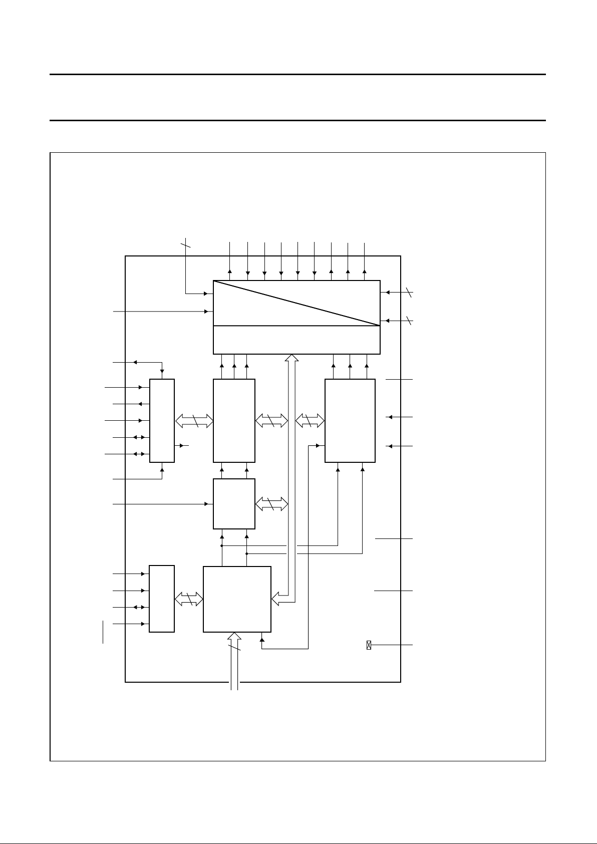
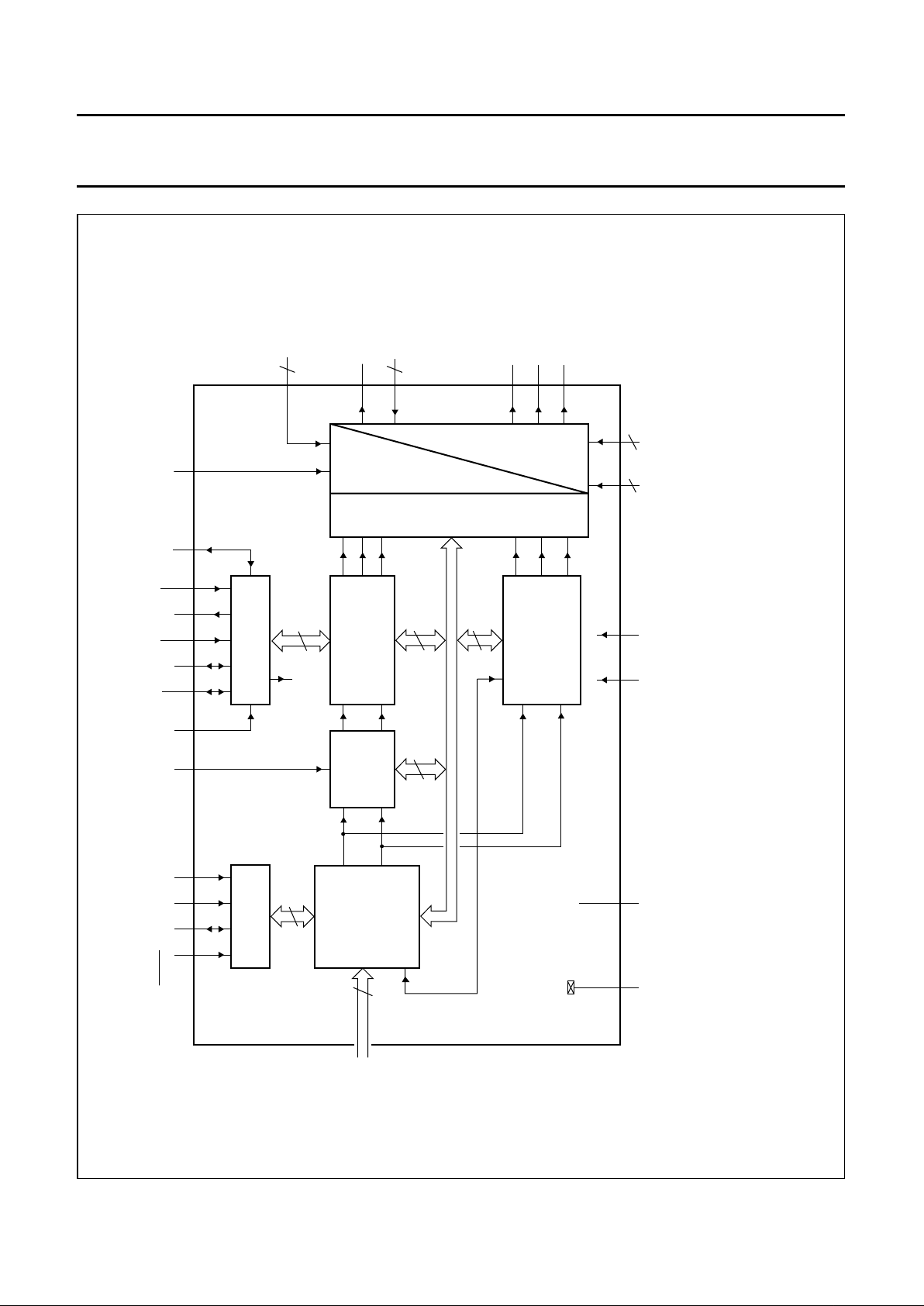
BLOCK DIAGRAM
ll pagewidth
MGG550
8
2
8
I
2
C-BUS
INTERFACE
I
2
C-bus
control
8
I
2
C-bus
control
8
I
2
C-bus
control
8
22
I
2
C-bus
control
I
2
C-bus
control
I
2
C-bus
control
8
I
2
C-bus
control
DATA
MANAGER
ENCODER
SYNC CLOCK
OUTPUT
INTERFACE
MODE
RGB
PROCESSOR
internal
control bus
CbCr
Y
C
clock
and timing
D
A
1
84
83
4
37 50
35
36
46
45 44
48
54, 57, 60,
64, 74
53, 75
73
67
62
59
56
65
61
58
55
63, 6852, 76
7778
3, 15, 24,
30, 39, 42,
51, 79, 81
5, 14, 22,
29, 38, 41,
49, 80, 82
2, 16 to 21, 23,
40, 43, 47, 66,
70, 72
Y
CbCr
25 to 28,
31 to 34
MP7
to
MP0
RESET
SDA
SCL
SA
RTCI
CDIR
RCV1
RCV2
V
DDDO
(5)
XTALO
XTALI
LLC
V
DDA1
to V
DDA5
V
refH1VrefH2
CVBS
(1)
V
SSA1
res
res
res
res
RED
(2)
GREEN
(3)
BLUE
(4)
CUR1
CUR2
V
refL1VrefL2
AP
69, 71
resSPn.c.
V
DDD1
to
V
DDD9
V
SSD1
to
V
SSD9
Y
SAA7124
SAA7125
Fig.1 Block diagram; PLCC84.
(1) Alternatively Y or CVBS.
(2) Alternatively CHROMA or Cr.
(3) Alternatively CVBS or Yin.
(4) Alternatively CVBS or Cb.
(5) V1 devices only.
1996 Nov 07 5
Philips Semiconductors Preliminary specification
Digital Video Encoder (ECO-DENC) SAA7124; SAA7125
ll pagewidth
MGG551
8
2
8
I
2
C-BUS
INTERFACE
I
2
C-bus
control
8
I
2
C-bus
control
8
I
2
C-bus
control
8
22
I
2
C-bus
control
I
2
C-bus
control
I
2
C-bus
control
8
I
2
C-bus
control
DATA
MANAGER
ENCODER
SYNC CLOCK
OUTPUT
INTERFACE
MODE
RGB
PROCESSOR
internal
control bus
CbCr
Y
C
clock
and timing
D
A
57
56
55
59
21 31
19
20
28
27 26
29
34, 36, 38,
41, 46
33, 47
45
42,
43
39
37
35
40, 4432, 48
4950
6, 8, 14,
23, 25, 51,
53, 58
5, 7, 13,
22, 24, 30,
52, 54, 60
Y
CbCr
9 to 12,
15 to 18
MP7
to
MP0
RESET
SDA
SCL
SA
RTCI
CDIR
RCV1
RCV2
V
DDDO
XTALO
XTALI
LLC
V
DDA1
to V
DDA5
V
refH1VrefH2
CVBS
(1)
V
SSA2
RED
(2)
GREEN
(3)
BLUE
(4)
CUR1
CUR2
V
refL1VrefL2
APSP
V
DDD1
to
V
DDD9
V
SSD1
to
V
SSD8
Y
SAA7124
SAA7125
2
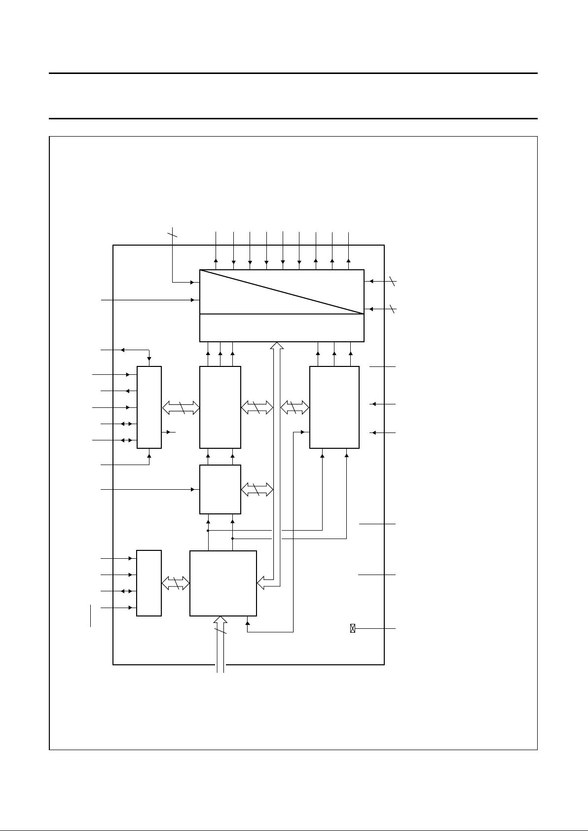
Fig.2 Block diagram; TQFP64, V1 devices only.
(1) Alternatively Y or CVBS.
(2) Alternatively CHROMA or Cr.
(3) Alternatively CVBS or Yin.
(4) Alternatively CVBS or Cb.
1996 Nov 07 6
Philips Semiconductors Preliminary specification
Digital Video Encoder (ECO-DENC) SAA7124; SAA7125
gewidth
MGG552
8
2
8
I
2
C-BUS
INTERFACE
I
2
C-bus
control
8
I
2
C-bus
control
8
I
2
C-bus
control
8
22
I
2
C-bus
control
I
2
C-bus
control
I
2
C-bus
control
8
I
2
C-bus
control
DATA
MANAGER
ENCODER
SYNC CLOCK
OUTPUT
INTERFACE
MODE
RGB
PROCESSOR
internal
control bus
CbCr
Y
C
clock
and timing
D
A
73
72
71
75
27 38
25
26
34
33 32
36
54, 57, 60,
64, 74
53, 75
61
55
54
51
48
45
50
47
44
52, 5641, 64
6566
6, 14, 20,
29, 31, 39,
67, 69, 74
5, 13, 19,
28, 30, 37,
68, 70, 76
7 to 12, 35, 40
58, 60
Y
CbCr
15 to 18,
21 to 24
MP7
to
MP0
RESET
SDA
SCL
SA
RTCI
CDIR
RCV1
RCV2
V
DDDO
(5)
XTALO
XTALI
LLC
V
DDA1
to V
DDA5
V
refH1VrefH2
CVBS
(1)
V
SSA1
res
res
res
res
RED
(2)
GREEN
(3)
BLUE
(4)
CUR1
CUR2
V
refL1VrefL2
AP
57, 59
resSPn.c.
V
DDD1
to
V
DDD9
V
SSD1
to
V
SSD9
Y
SAA7124
SAA7125
Fig.3 Block diagram; QFP80.
(1) Alternatively Y or CVBS.
(2) Alternatively CHROMA or Cr.
(3) Alternatively CVBS or Yin.
(4) Alternatively CVBS or Cb.
(5) V1 devices only.
1996 Nov 07 7
Philips Semiconductors Preliminary specification
Digital Video Encoder (ECO-DENC) SAA7124; SAA7125
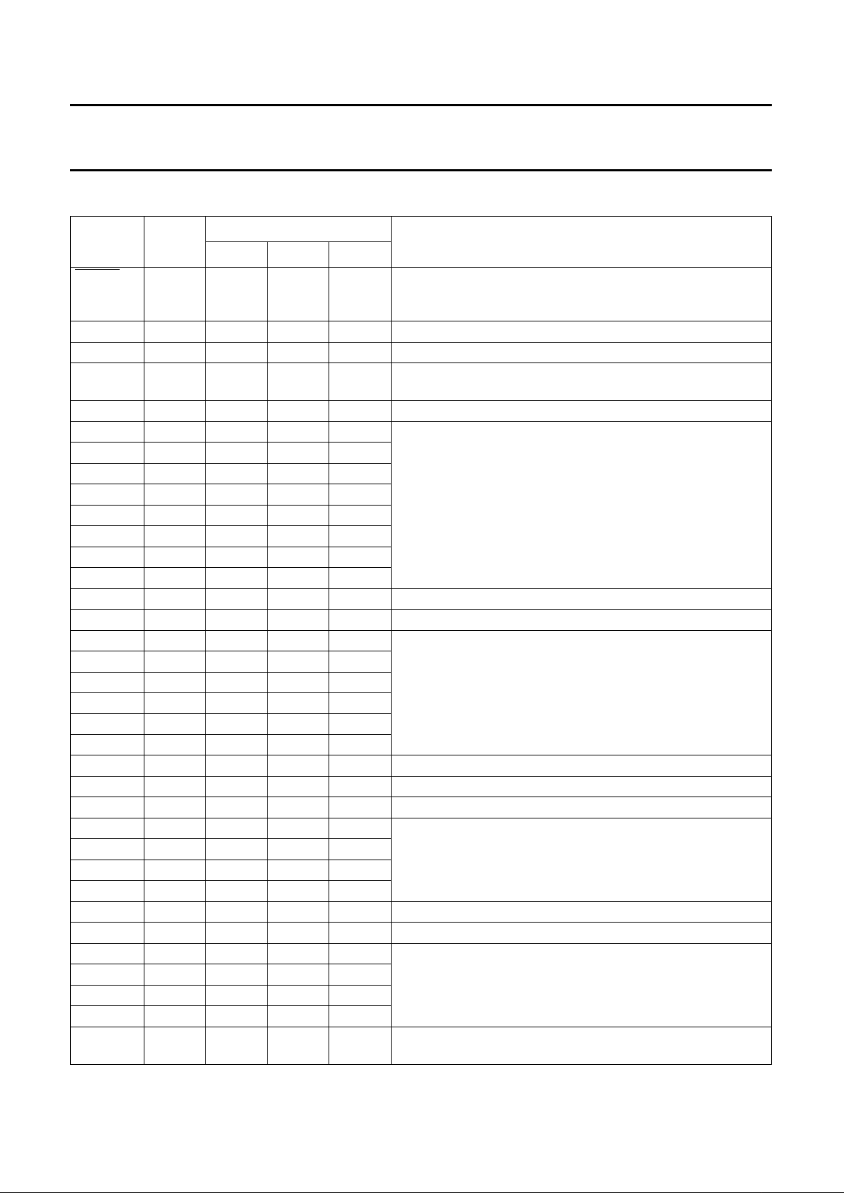
PINNING
SYMBOL TYPE
PIN
DESCRIPTION
PLCC84 LQFP64 QFP80
RESET I 1 57 73 Reset input, active LOW. After reset is applied, all digital I/Os
are in input mode. The I2C-bus receiver waits for the START
condition.
n.c. − 2 −−not connected
V
SSD1
I 3 6 6 digital ground 1
SA I 4 59 75 The I
2
C-bus slave address select input pin. LOW: slave
address = 88H, HIGH = 8CH.
V
DDD1
I 5 5 5 digital supply voltage 1
TP1 O 6 61 77
Test pin outputs. Leave open for normal operation.
TP2 O 7 62 78
TP3 O 8 63 79
TP4 O 9 64 80
TP5 O 10 1 1
TP6 O 11 2 2
TP7 O 12 3 3
TP8 O 13 4 4
V
DDD2
I 14 7 13 digital supply voltage 2
V
SSD2
I 15 8 14 digital ground 2
n.c. − 16 − 7
not connected
n.c. − 17 − 8
n.c. − 18 − 9
n.c. − 19 − 10
n.c. − 20 − 11
n.c. − 21 − 12
V
DDD3
I 22 13 19 digital supply voltage 3
n.c. − 23 −−not connected
V
SSD3
I 24 14 20 digital ground 3
MP7 I 25 9 15
Upper 4 bits of MPEG port. It is an input for
“CCIR 656”
style
multiplexed Cb, Y, Cr data.
MP6 I 261016
MP5 I 27 11 17
MP4 I 281218
V
DDD4
I 29 22 28 digital supply voltage 4
V
SSD4
I 30 23 29 digital ground 4
MP3 I 311521
Lower 4 bits of MPEG port. It is an input for
“CCIR 656”
style
multiplexed Cb, Y, Cr data.
MP2 I 321622
MP1 I 331723
MP0 I 341824
RCV1 I/O 35 19 25 Raster Control 1 for video port. This pin receives/provides a
VS/FS/FSEQ signal.
1996 Nov 07 8
Philips Semiconductors Preliminary specification
Digital Video Encoder (ECO-DENC) SAA7124; SAA7125
RCV2 I/O 36 20 26 Raster Control 2 for video port. This pin provides an HS pulse
of programmable length or receives an HS pulse.
RTCI I 37 21 27 Real Time Control input. If the LLC clock is provided by an
SAA7111 or SAA7151B, RTCI should be connected to the
RTCO pin of the respective decoder to improve the signal
quality.
V
DDD5
I 38 24 30 digital supply voltage 5
V
SSD5
I 39 25 31 digital ground 5
n.c. − 40 − 35 not connected
V
DDD6
I 41 30 37 digital supply voltage 6
V
SSD6
I 42 51 39 digital ground 6
n.c. − 43 − 40 not connected
XTALI I 44 26 32 Crystal oscillator input (from crystal). If the oscillator is not
used, this pin should be connected to ground.
XTALO O 45 27 33 Crystal oscillator output (to crystal).
V
DDDO
I 46 28 34 digital supply voltage for the internal oscillator; note 1
n.c. − 47 −−not connected
LLC I/O 48 29 36 Line-Locked Clock. This is the 27 MHz master clock for the
encoder. The I/O direction is set by the CDIR pin.
V
DDD7
I 49 52 68 digital supply voltage 7
CDIR I 50 31 38 Clock direction. If CDIR input is HIGH, the circuit receives a
clock signal, otherwise if CDIR is LOW, LLC is generated by
the internal crystal oscillator.
V
SSD7
I 51 53 67 digital ground 7
V
refL1
I 52 32 41 Lower reference voltage 1 input for DACs; connect to analog
ground.
V
refH1
I 53 33 42 Upper reference voltage 1 input for DACs; connect via 100 nF
capacitor to analog ground.
V
DDA1
I 54 34 43 Analog supply voltage 1 for DACs.
BLUE O 55 35 44 Analog output of the BLUE component.
res I 56 − 45 reserved
V
DDA2
I 57 36 46 Analog supply voltage 2 for DACs.
GREEN O 58 37 47 Analog output of GREEN component.
res I 59 − 48 reserved
V
DDA3
I 60 38 49 Analog supply voltage 3 for DACs.
RED O 61 39 50 Analog output of RED component.
res I 62 − 51 reserved
CUR1 I 63 40 52 Current input 1 for RGB amplifiers; connect via 15 kΩ resistor
to V
DDA
.
V
DDA4
I 64 41 53 Analog supply voltage 4 for DACs.
res I 65 − 54 reserved
n.c. − 66 −−not connected
SYMBOL TYPE
PIN
DESCRIPTION
PLCC84 LQFP64 QFP80
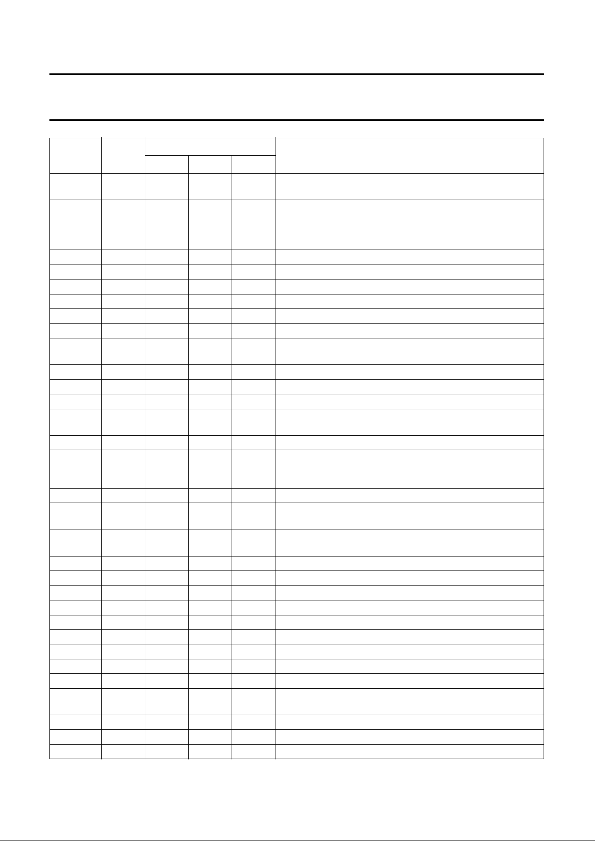
1996 Nov 07 9
Philips Semiconductors Preliminary specification
Digital Video Encoder (ECO-DENC) SAA7124; SAA7125
Note
1. V1 devices only.
V
SSA1
I 67 42 55 Analog ground 1 for the DACs.
V
SSA2
I − 43 − Analog ground 2 for the DACs.
CUR2 I 68 44 56 Current input 2 for RGB amplifiers; connect via 15 kΩ resistor
to V
DDA
.
res O 69 − 57 reserved
n.c. − 70 − 58 not connected
res O 71 − 59 reserved
n.c. − 72 − 60 not connected
CVBS O 73 45 61 Analog output of the CVBS signal.
V
DDA5
I 74 46 62 Analog supply voltage 5 for DACs.
V
refH2
I 75 47 63 Upper reference voltage 2 input for DACs; connect via 100 nF
capacitor to analog ground.
V
refL2
I 76 48 64 Lower reference voltage 2 input for DACs; connect to analog
ground.
AP I 77 49 65 Test pin. Connected to digital ground for normal operation.
SP I 78 50 66 Test pin. Connected to digital ground for normal operation.
V
SSD8
I 79 58 69 digital ground 8
V
DDD8
I 80 54 70 digital supply voltage 8
V
SSD9
I81−74 digital ground 9
V
DDD9
I 82 60 76 digital supply voltage 9
SCL I 835571I
2
C-bus serial clock input.
SDA I/O 84 56 72 I
2
C-bus serial data input/output.
SYMBOL TYPE
PIN
DESCRIPTION
PLCC84 LQFP64 QFP80
1996 Nov 07 10
Philips Semiconductors Preliminary specification
Digital Video Encoder (ECO-DENC) SAA7124; SAA7125
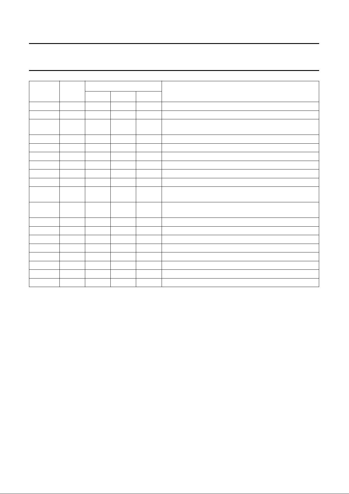
Fig.4 Pin configuration; PLCC84.
(1) V1 devices only.
handbook, full pagewidth
SAA7124
SAA7125
MGG548
12
13
14
15
16
17
18
19
20
21
22
23
24
25
26
27
28
29
30
31
32
74
73
72
71
70
69
68
67
66
65
64
63
62
61
60
59
58
57
56
55
54
33
34
35
36
37
38
39
40
41
42
43
44
45
46
47
48
49
50
51
52
53
11
10
9
8
7
6
5
4
3
2
1
84
83
82
81
80
79
78
77
76
75
TP6
TP5
TP4
TP3
TP2
TP1
V
DDD1
SA
V
SSD1
n.c.
RESET
SDA
SCL
V
DDD9VSSD9VDDD8VSSD8
SP
AP
V
refL2VrefH2
MP1
MP0
RCV1
RCV2
RTCI
V
DDD5
V
SSD5
n.c.
V
DDD6
V
SSD6
n.c.
XTALI
XTALO
V
DDDO
(1)
n.c.
LLC
V
DDD7
CDIR
V
SSD7
V
refL1
V
ref H1
V
DDA5
CVBS
n.c.
res
n.c.
res
CUR2
V
SSA1
n.c.
res
V
DDA4
CUR1
res
RED
V
DDA3
res
GREEN
V
DDA2
res
BLUE
V
DDA1
TP7
TP8
V
DDD2
V
SSD2
n.c.
n.c.
n.c.
n.c.
n.c.
n.c.
V
DDD3
n.c.
V
SSD3
MP7
MP6
MP5
MP4
V
DDD4
V
SSD4
MP3
MP2
1996 Nov 07 11
Philips Semiconductors Preliminary specification
Digital Video Encoder (ECO-DENC) SAA7124; SAA7125
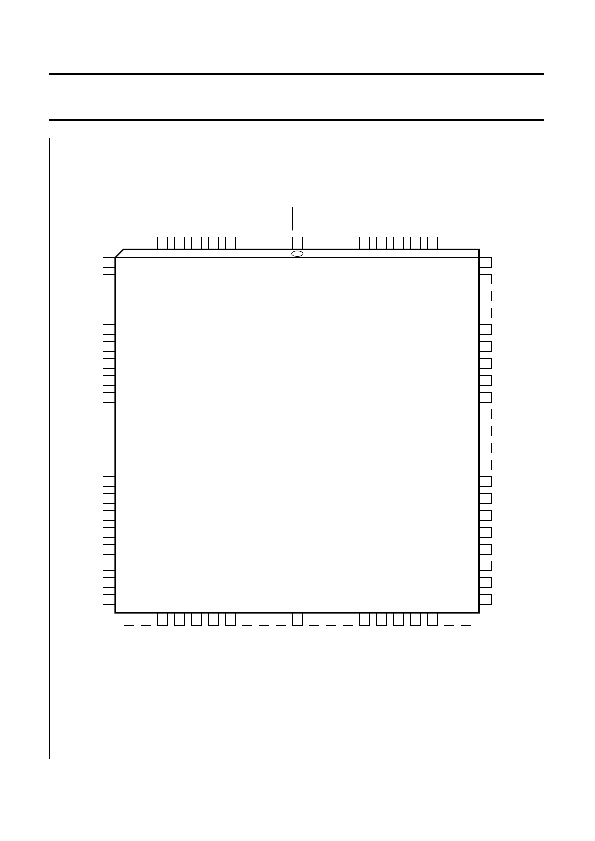
Fig.5 Pin configuration; LQFP64 (V1 devices only).
handbook, full pagewidth
SAA7124
SAA7125
MGG547
1
2
3
4
5
6
7
8
9
10
11
12
13
14
15
16
48
47
46
45
44
43
42
41
40
39
38
37
36
35
34
33
V
refL2
V
refH2
V
DDA5
CVBS
CUR2
V
SSA2
V
SSA1
V
DDA4
CUR1
RED
V
DDA3
GREEN
V
DDA2
BLUE
V
DDA1
V
refH1
TP5
TP6
TP7
TP8
V
DDD1
V
SSD1
V
DDD2
V
SSD2
MP7
MP6
MP5
MP4
V
DDD3
V
SSD3
MP3
MP2
17
18
19
20
21
22
23
24
25
26
27
28
29
30
31
32
64
63
62
61
60
59
58
57
56
55
54
53
52
51
50
49
TP4
TP3
TP2
TP1
V
DDD9
SA
V
SSD8
RESET
SDA
SCL
V
DDD8
V
SSD7
V
DDD7
V
SSD6
SP
AP
MP1
MP0
RCV1
RCV2
RTCI
V
DDD4
V
SSD4
V
DDD5
V
SSD5
XTALI
XTALO
V
DDDO
LLC
V
DDD6
CDIR
V
refL1
1996 Nov 07 12
Philips Semiconductors Preliminary specification
Digital Video Encoder (ECO-DENC) SAA7124; SAA7125
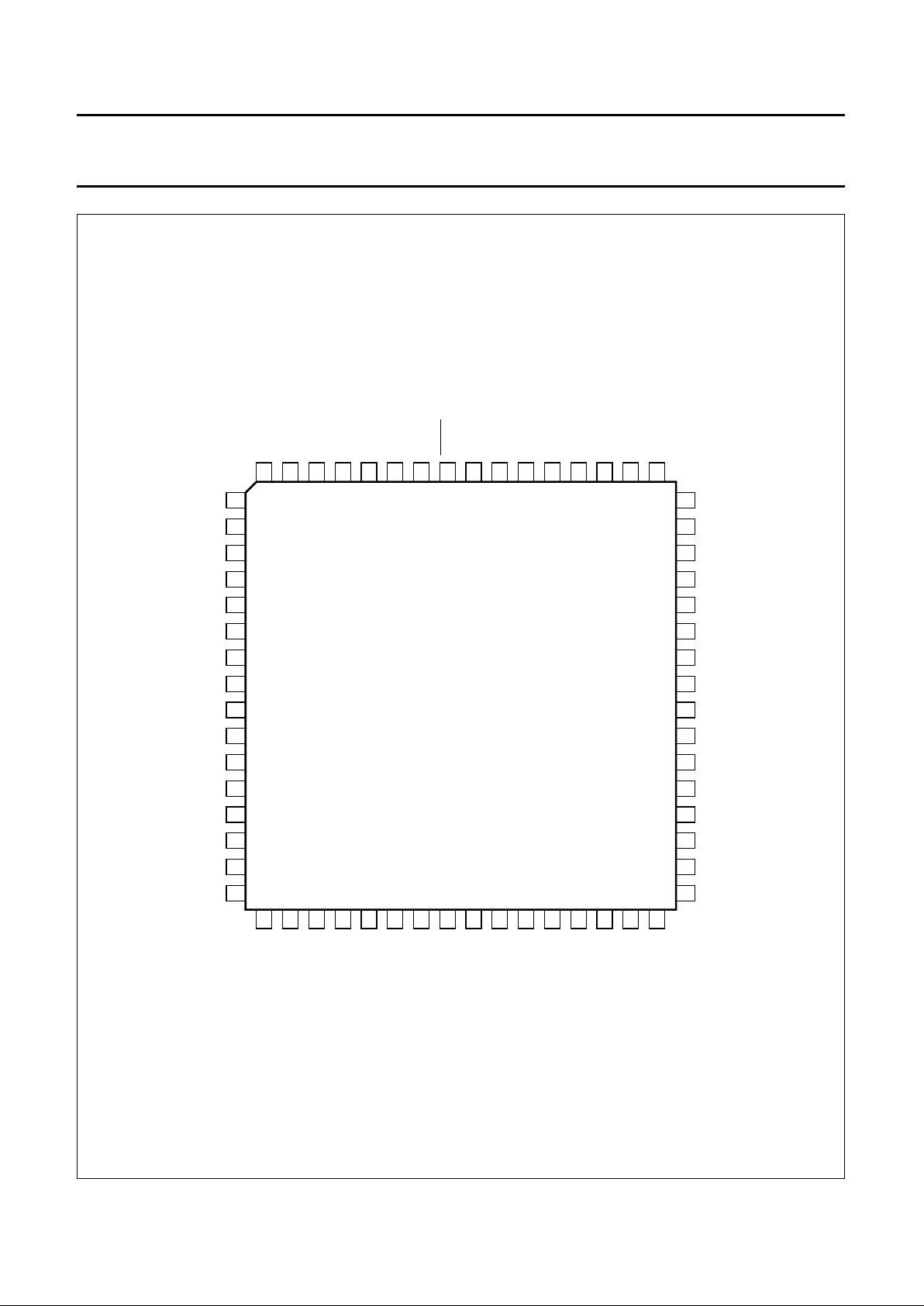
Fig.6 Pin configuration; QFP80.
(1) V1 devices only.
handbook, full pagewidth
SAA7124
SAA7125
MGG549
1
2
3
4
5
6
7
8
9
10
11
12
13
14
15
16
17
18
19
20
60
59
58
57
56
64
63
62
61
55
54
53
52
51
50
49
48
47
46
45
44
43
42
41
n.c.
res
n.c.
res
CUR2
V
refL2
V
refH2
V
DDA5
CVBS
V
SSA1
res
V
DDA4
CUR1
res
RED
V
DDA3
res
GREEN
V
DDA2
res
BLUE
V
DDA1
V
refH1
V
refL1
V
DDD1
V
SSD1
n.c.
n.c.
n.c.
TP5
TP6
TP7
TP8
n.c.
n.c.
n.c.
V
DDD2
V
SSD2
MP7
MP6
MP5
MP4
V
DDD3
V
SSD3
MP3
MP2
MP1
MP0
21
22
23
24
25
26
27
28
29
30
31
32
33
34
35
36
37
38
39
40
RCV1
RCV2
RTCI
V
DDD4
V
SSD4
V
DDD5
V
SSD5
XTALI
XTALO
V
DDDO
(1)
n.c.
LLC
V
DDD6
CDIR
V
SSD6
n.c.
TP4
TP3
TP2
TP1
V
DDD9
SA
V
SSD9
RESET
SDA
SCL
V
DDD8VSSD8VDDD7VSSD7
SP
AP
80
79
78
77
76
75
74
73
72
71
70
69
68
67
66
65

1996 Nov 07 13
Philips Semiconductors Preliminary specification
Digital Video Encoder (ECO-DENC) SAA7124; SAA7125
FUNCTIONAL DESCRIPTION
The digital video encoder (ECO-DENC) encodes digital
luminance and colour difference signals into analog CVBS
and simultaneously RGB signals. NTSC-M, PAL B/G
standards and sub-standards are supported.
Both interlaced and non-interlaced operation is possible
for all standards.
Optionally, the input Y, Cb and Cr data, digital-to-analog
converted, is available at the analog RGB outputs.
For applications that do not require RGB output, the device
can be configured in such a way that S-Video and twice
CVBS is available (Y at CVBS-DAC, C at R-DAC, and
CVBS at G-DAC and B-DAC).
The basic encoder function consists of subcarrier
generation, colour modulation and insertion of
synchronization signals. Luminance and chrominance
signals are filtered in accordance with the standard
requirements of
“RS-170-A”
and
“CCIR 624”
.
For ease of analog post filtering the signals are twice
oversampled with respect to the pixel clock before
digital-to-analog conversion.
For total filter transfer characteristics see
Figs 7, 8, 9, 10, 11 and 12. The DACs for Y, C, and CVBS
are realized with full 10-bit resolution, DACs for RGB with
9-bit resolution.
The MPEG port (MP) accepts 8 line multiplexed Cb, Y, Cr
data.
The 8-bit multiplexed Cb-Y-Cr formats are
“CCIR 656”
(D1 format) compatible, but auxiliary codes such as SAV
and EAV are decoded optionally for trigger purposes.
A crystal-stable master clock (LLC) of 27 MHz, which is
twice the CCIR line-locked pixel clock of 13.5 MHz, needs
to be supplied externally. Optionally, a crystal oscillator
input/output pair of pins and an on-chip clock driver is
provided.
It is also possible to connect a Philips Digital Video
Decoder (SAA7111 or SAA7151B) in conjunction with a
CREF clock qualifier to ECO-DENC. Via the RTCI pin,
connected to RTCO of a decoder, information concerning
actual subcarrier, PAL-ID, and if connected to SAA7111,
definite subcarrier phase can be inserted.
The ECO-DENC synthesizes all necessary internal
signals, colour subcarrier frequency, and synchronization
signals, from that clock.
The encoder can be configured as slave with respect to
RCV trigger inputs or auxiliary
“CCIR 656”
codes, or can
be master to output horizontal and vertical trigger pulses.
The IC also contains Closed Caption and Extended Data
Services Encoding (Line 21), and supports anti-taping
signal generation in accordance with Macrovision.
A number of possibilities are provided for setting different
video parameters such as:
Black and blanking level control
Colour subcarrier frequency
Variable burst amplitude etc.
During reset (RESET = LOW) and after reset is released,
all digital I/O stages are set to input mode. A reset forces
the I2C-bus interface to abort any running bus transfer and
sets register 3A to 03H, register 61 to 06H and
registers 6BH and 6EH to 00H. All other control registers
are not influenced by a reset.
Data manager
In the data manager, real time arbitration on the data
stream to be encoded is performed.
Optionally, the device can operate as a 100/75 colour bar
test pattern generator without need for an external data
source.
Encoder
V
IDEO PATH
The encoder generates out of Y, U and V baseband
signals luminance and colour subcarrier output signals,
suitable for use as CVBS or separate Y and C signals.
Luminance is modified in gain and in offset (latter
programmable in a certain range to enable different black
level set-ups). After having been inserted a fixed
synchronization level, in accordance with standard
composite synchronization schemes, and blanking level,
programmable also in a certain range to allow for
manipulations with Macrovision anti-taping, additional
insertion of AGC super-white pulses, programmable in
height, is supported.
In order to enable easy analog post filtering, luminance is
interpolated from 13.5 MHz data rate to 27 MHz data rate,
providing luminance in 10-bit resolution. This filter is also
used to define smoothed transients for synchronization
pulses and blanking period. For transfer characteristic of
the luminance interpolation filter see Figs 9 and 10.
1996 Nov 07 14
Philips Semiconductors Preliminary specification
Digital Video Encoder (ECO-DENC) SAA7124; SAA7125
Chrominance is modified in gain (programmable
separately for U and V), standard dependent burst is
inserted, before baseband colour signals are interpolated
from 6.75 MHz data rate to 27 MHz data rate. One of the
interpolation stages can be bypassed, thus providing a
higher colour bandwidth, which can be made use of for
Y and C output. For transfer characteristics of the
chrominance interpolation filter see Figs 7 and 8.
The amplitude of inserted burst is programmable in a
certain range, suitable for standard signals and for special
effects. Behind the succeeding quadrature modulator,
colour in 10-bit resolution is provided on subcarrier.
The numeric ratio between Y and C outputs is in
accordance with set standards.
C
LOSED CAPTION ENCODER
Using this circuit, data in accordance with the specification
of Closed Caption or Extended Data Service, delivered by
the control interface, can be encoded (Line 21).
Two dedicated pairs of bytes (two bytes per field), each
pair preceded by run-in clocks and framing code, are
possible.
The actual line number where data is to be encoded in, can
be modified in a certain range.
Data clock frequency is in accordance with definition for
NTSC-M standard 32 times horizontal line frequency.
Data LOW at the output of the DACs corresponds to 0 IRE,
data HIGH at the output of the DACs corresponds to
approximately 50 IRE.
It is also possible to encode Closed Caption Data for 50 Hz
field frequencies at 32 times horizontal line frequency.
A
NTI-TAPING (SAA7124 ONLY)
For more information contact your nearest Philips
Semiconductors sales office.
RGB processor
This block contains a dematrix in order to produce RED,
GREEN and BLUE signals to be fed to a SCART plug.
Before Y, Cb and Cr signals are de-matrixed, 2 times
oversampling for luminance and 4 times oversampling for
colour difference signals is performed. For transfer curves
of luminance and colour difference components of RGB
see Figs 11 and 12.
Output interface/DACs
In the output interface encoded both Y and C signals are
converted from digital-to-analog in 10-bit resolution.
Y and C signals are also combined to a 10-bit CVBS
signal.
RED, GREEN and BLUE signals (optionally Cr, Y, Cb) are
also converted from digital-to-analog, each providing a
9-bit resolution.
All output occurs with the same processing delay.
Absolute amplitudes at the input of the DAC for CVBS is
reduced by
15
⁄16with respect to Y and C DACs to make
maximum use of conversion ranges.
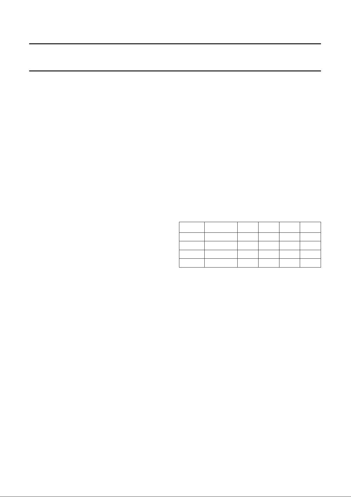
Depending on control bits YC_EN and DEMOFF, different
signal combinations are available at DACs #1 to #4.
YC_EN = DEMOFF = LOW is the default configuration
after reset.
Table 1 Control of DAC signals
Outputs of the DACs can be set together in two groups
(#1 and #2 by DOWNB, #3 and #4 by DOWNA) via
software control to minimum output voltage for either
purpose.
Synchronization
Synchronization of the ECO-DENC is able to operate in
two modes; slave mode and master mode.
In the slave mode, the circuit accepts synchronization
pulses at the bidirectional RCV1 port (or equivalently as
frame synchronization from
“CCIR 656”
data stream).
The timing and trigger behaviour related to RCV1 can be
influenced by programming the polarity and on-chip delay
of RCV1. Active slope of RCV1 defines the vertical phase
and optionally the odd/even and colour frame phase to be
initialized, it can be also used to set the horizontal phase.
If the horizontal phase is not to be influenced by RCV1, a
horizontal pulse needs to be supplied at the RCV2 pin
(or a horizontal synchronization from
“CCIR 656”
data
stream). Timing and trigger behaviour can also be
influenced for RCV2.
YC_EN DEMOFF DAC1 DAC2 DAC3 DAC4
0 0 CVBS R G B
0 1 CVBS Cr Y Cb
1 0 VBS C CVBS CVBS
1 1 VBS C CVBS CVBS
 Loading...