

Philips saa7120, saa7121 DATASHEETS

INTEGRATED CIRCUITS
DATA SH EET
SAA7120; SAA7121
Digital Video Encoder (ConDENC)
Preliminary specification
File under Integrated Circuits, IC22
1997 Jan 06
Philips Semiconductors Preliminary specification
Digital Video Encoder (ConDENC) SAA7120; SAA7121
FEATURES
• Monolithic CMOS 3.3 V (5 V) device
• Digital PAL/NTSC encoder
• System pixel frequency 13.5 MHz
• Accepts MPEG decoded data on 8-bit wide input port;
input data format Cb-Y-Cr (CCIR 656), SAV and EAV
• Three DACs for Y, C and CVBS, two times oversampled
with 10 bit resolution
• Real time control of subcarrier
• Cross colour reduction filter
• Closed captioning encoding and WST- and
NABTS-Teletext encoding including sequencer and filter
• Line 23 wide screen signalling encoding
2
• Fast I
C-bus control port (400 kHz)
• Encoder can be master or slave
• Programmable horizontal and vertical input
synchronization phase
• Programmable horizontal sync output phase
• Internal colour bar generator (CBG)
• 2 × 2 bytes in lines 20 (NTSC) for copy guard
management system can be loaded via I2C-bus
• Down-mode of DACs
• Controlled rise/fall times of synchronization and
blanking output signals
• Macrovision Pay-per-View copy protection system rev.7
and rev.6.1 as option.
This applies to SAA7120 only. The device is protected
by USA patent numbers 4631603, 4577216 and
4819098 and other intellectual property rights. Use of
the Macrovision anti-copy process in the device is
licensed for non-commercial home use only.
Reverse engineering or disassembly is prohibited.
Please contact your nearest Philips Semiconductors
sales office for more information.
• QFP44 package.
GENERAL DESCRIPTION
The SAA7120; SAA7121 encodes digital YUV video data
to an NTSC or PAL CVBS or S-Video signal.
The circuit accepts CCIR compatible YUV data with
720 active pixels per line in 4:2:2multiplexed formats,
for example MPEG decoded data. It includes a sync/clock
generator and on-chip DACs.
QUICK REFERENCE DATA
SYMBOL PARAMETER MIN. TYP. MAX. UNIT
V
V
I
DDA
I
DDD
V
V
DDA
DDD
i
o(p-p)
analog supply voltage 3.1 3.3 3.5 V
digital supply voltage 3.0 3.3 3.6 V
analog supply current −−62 mA
digital supply current −−38 mA
input signal voltage levels TTL compatible
analog output signal voltages Y, C, and CVBS without load
1.2 1.35 1.45 V
(peak-to-peak value)
R
L
load resistance 75 − 300 Ω
ILE LF integral linearity error −−±3 LSB
DLE LF differential linearity error −−±1 LSB
T
amb
operating ambient temperature 0 − +70 °C
1997 Jan 06 2
Philips Semiconductors Preliminary specification
Digital Video Encoder (ConDENC) SAA7120; SAA7121
ORDERING INFORMATION
TYPE
NUMBER
SAA7120;
SAA7121
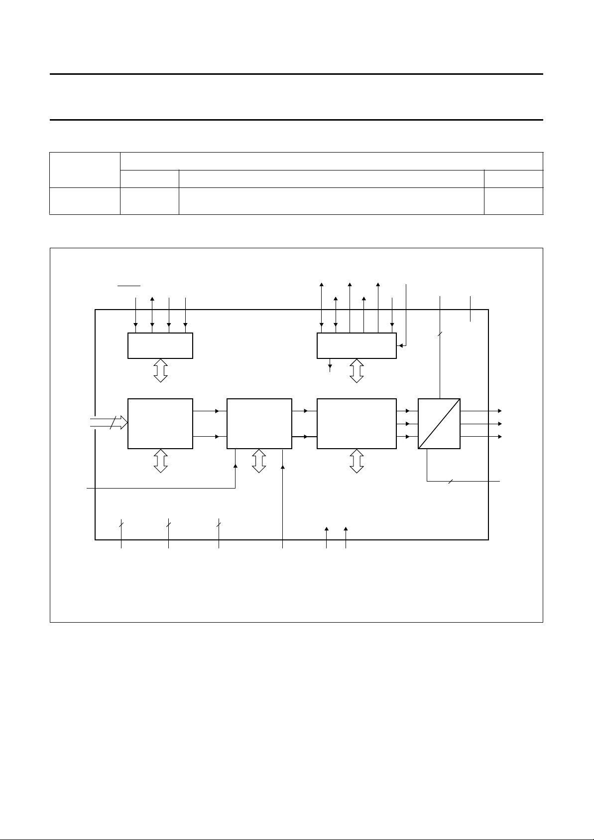
BLOCK DIAGRAM
handbook, full pagewidth
RESET SDA SCL
9 to 16
MP7
to
MP0
PACKAGE
NAME DESCRIPTION VERSION
QFP44 plastic quad flat package; 44 leads (lead length 2.35 mm);
SOT307-2
body 10 × 10 × 1.75 mm
V
DDA1,
V
DDA2
V
DDA3
D
,
25, 28,
31
A
V
DDA4
368433734
30
CVBS
27
Y
24
C
SA
40 42 41 21
I2C-BUS
INTERFACE
2
I
C-bus
control
DATA
MANAGER
Y
CbCr
SAA7120
SAA7121
ENCODER
Y
C
RCV1
RCV2
7
clock
and timing
INTERFACE
TTXRQ
XCLK
SYNC
CLOCK
OUTPUT
XTALO
2
C-bus
I
control
LLC
XTALI
35 4
TTX
I2C-bus
control
1, 20, 22,
23, 26, 29
I2C-bus
control
219 3
SPRTCI AP
44
V
SSD1,
V
SSD2
V
SSD3
5, 18, 38
,
V
DDD1,
V
DDD2
V
DDD3
6, 17, 39
res.
,
I2C-bus
control
32, 33
MBH787
V
SSA1
V
SSA2
Fig.1 Block diagram.
1997 Jan 06 3
Philips Semiconductors Preliminary specification
Digital Video Encoder (ConDENC) SAA7120; SAA7121
PINNING
SYMBOL PIN I/O DESCRIPTION
res. 1 − reserved
SP 2 I test pin; connected to digital ground for normal operation
AP 3 I test pin; connected to digital ground for normal operation
LLC 4 I line-locked clock; this is the 27 MHz master clock for the encoder
V
SSD1
V
DDD1
RCV1 7 I/O raster control 1 for video port; this pin receives/provides a VS/FS/FSEQ signal
RCV2 8 I/O raster control 2 for video port; this pin provides an HS pulse of programmable length or
MP7 9 I
MP6 10 I
MP5 11 I
MP4 12 I
MP3 13 I
MP2 14 I
MP1 15 I
MP0 16 I
V
DDD2
V
SSD2
RTCI 19 I Real Time Control input; if the LLC clock is provided by an SAA7111 or SAA7151B,
res. 20 − reserved
SA 21 I the I
res. 22 − reserved
res. 23 − reserved
C 24 O analog output of the chrominance signal
V
DDA1
res. 26 − reserved
Y 27 O analog output of VBS signal
V
DDA2
res. 29 − reserved
CVBS 30 O analog output of the CVBS signal
V
DDA3
V
SSA1
V
SSA2
XTALO 34 O crystal oscillator output (to crystal)
XTALI 35 I crystal oscillator input (from crystal); if the oscillator is not used, this pin should be
V
DDA4
XCLK 37 O clock output of the crystal oscillator
5 I digital ground 1
6 I digital supply voltage 1
receives an HS pulse
MPEG port; it is an input for
“CCIR 656”
style multiplexed Cb Y, Cr data
17 I digital supply voltage 2
18 I digital ground 2
RTCI should be connected to pin RTCO of the decoder to improve the signal quality
2
C-bus slave address select input pin; LOW: slave address = 88H, HIGH = 8CH
25 I analog supply voltage 1 for the C DAC
28 I analog supply voltage 2 for the Y DAC
31 I analog supply voltage 3 for the CVBS DAC
32 I analog ground 1 for the DACs
33 I analog ground 2 for the oscillator and reference voltage
connected to ground
36 I analog supply voltage 4 for the oscillator and reference voltage
1997 Jan 06 4
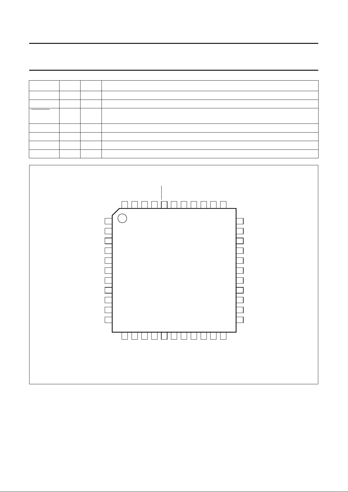
Philips Semiconductors Preliminary specification
Digital Video Encoder (ConDENC) SAA7120; SAA7121
SYMBOL PIN I/O DESCRIPTION
V
SSD3
V
DDD3
RESET 40 I reset input, active LOW; after reset is applied, all digital I/Os are in input mode;
SCL 41 I I
SDA 42 I/O I
TTXRQ 43 O teletext request output, indicating when bit stream is valid
TTX 44 I teletext bit stream input
handbook, full pagewidth
38 I digital ground 3
39 I digital supply voltage 3
the I2C-bus receiver waits for the START condition
2
C-bus serial clock input
2
C-bus serial data input/output
TTXRQ
SDA
44 TTX
43
42
SCL
41
RESET
40
DDD3
V
39
SSD3
V
38
XCLK
37
DDA4
V
36
XTALI
35
XTALO
34
V
SSD1
V
DDD1
RCV1
RCV2
SP
AP
LLC
MP7
MP6
MP5
1res.
2
3
4
5
6
7
8
9
10
11
12
13
14
MP4
MP3
MP2
SAA7120
SAA7121
15
MP1
16
MP0
17
DDD2
V
18
SSD2
V
19
RTCI
20
res.
21
SA
22
res.
33
32
31
30
29
28
27
26
25
24
23
MBH790
V
SSA2
V
SSA1
V
DDA3
CVBS
res.
V
DDA2
Y
res.
V
DDA1
C
res.
Fig.2 Pin configuration.
1997 Jan 06 5
Philips Semiconductors Preliminary specification
Digital Video Encoder (ConDENC) SAA7120; SAA7121
FUNCTIONAL DESCRIPTION
The digital video encoder (ConDENC) encodes digital
luminance and colour difference signals simultaneously
into analog CVBS and S-Video signals. NTSC-M,
PAL B/G, and sub-standards are supported.
Both interlaced and non-interlaced operation is possible
for all standards.
The basic encoder function consists of subcarrier
generation, colour modulation and the insertion of
synchronization signals. Luminance and chrominance
signals are filtered in accordance with the standard
requirements of
“RS-170-A”
and
“CCIR 624”
.
For ease of analog post-filtering the signals are
oversampled twice with respect to the pixel clock prior to
digital-to-analog conversion.
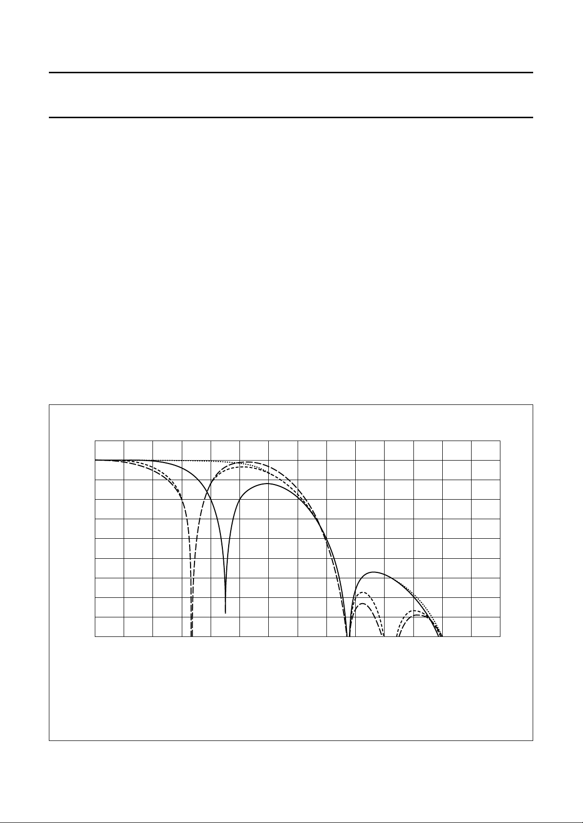
The filter characteristics are shown in Figs 3 and 4.
The DACs for Y, C, and CVBS have 10-bit resolution.
The 8-bit multiplexed Cb-Y-Cr formats are
“CCIR 656”
(D1 format) compatible, but the SAV and EAV codes can
be decoded optionally when the device is to operate in
slave mode.
It is also possible to connect a Philips Digital Video
Decoder (SAA7111 or SAA7151B) to the ConDENC.
Via pin RTCI, connected to RTCO of a decoder,
information concerning the actual subcarrier, PAL-ID and
(if used in conjunction with the SAA7111) the subcarrier
phase can be inserted.
The ConDENC synthesizes all necessary internal signals,
colour subcarrier frequency and synchronization signals.
2
Wide screen signalling data can be loaded via the I
C-bus.
It is inserted into line 23 for 50 Hz field rate standards.
The IC contains closed caption and extended data
services encoding (line 21), and supports anti-taping
signal generation in accordance with Macrovision.
Possibilities are provided for setting video parameters:
Black and blanking level control
Colour subcarrier frequency
Variable burst amplitude.
6
G
handbook, full pagewidth
v
(dB)
0
−6
−12
−18
−24
−30
−36
−42
−48
−54
024
(1) CCRS1 = 0; CCRS0 = 1.
(2) CCRS1 = 1; CCRS0 = 0.
(4)
(3)
(1)
6
(3) CCRS1 = 0; CCRS0 = 0.
(4) CCRS1 = 1; CCRS0 = 1.
MGD672
(2)
8101214
f (MHz)
Fig.3 Luminance transfer characteristic 1.
1997 Jan 06 6
Philips Semiconductors Preliminary specification
Digital Video Encoder (ConDENC) SAA7120; SAA7121
During reset (RESET = LOW) and after reset is released,
all digital I/O stages are set to input mode. A reset forces
handbook, halfpage
G
(dB)
1
v
0
MBE736
(1)
the I2C-bus interface to abort a running bus transfer and
sets register 3A to 03H, register 61 to 06H,
registers 6BH and 6EH to 00H and bit TTX60 to 0.
All other control registers are not influenced by a reset.
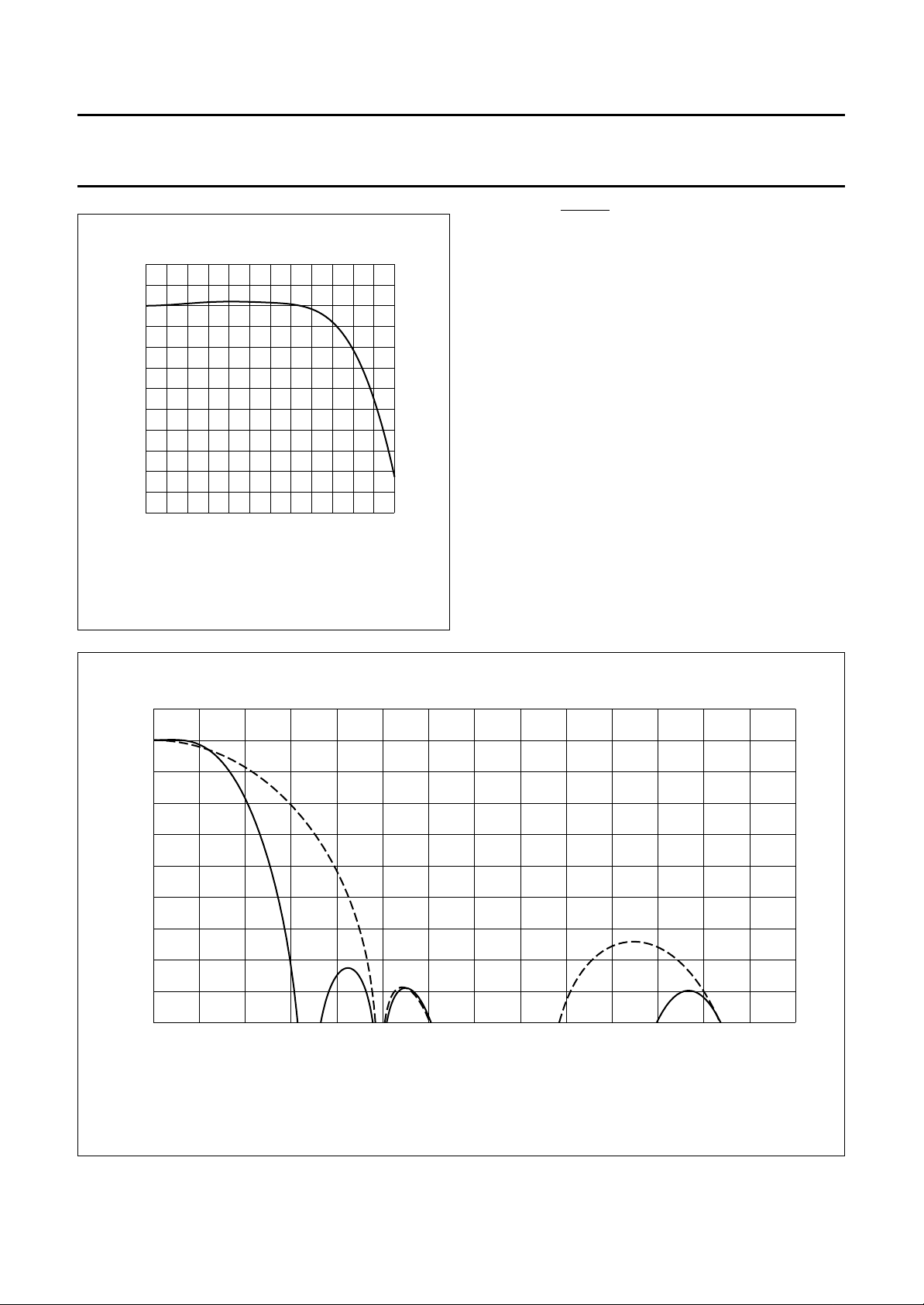
−1
−2
−3
−4
−5
02
(1) CCRS1 = 0; CCRS0 = 0.
4
Fig.4 Luminance transfer characteristic 2.
handbook, full pagewidth
G
(dB)
6
v
0
−6
f (MHz)
Encoder
IDEO PATH
V
The encoder generates out of Y, U and V baseband
signals luminance and colour subcarrier output signals,
suitable for use as CVBS or separate Y and C signals.
Luminance is modified in gain and in offset (the latter
programmable in a certain range to enable different black
level set-ups). A fixed synchronization level in accordance
6
with standard composite synchronization schemes is
inserted. The inserted blanking level is programmable to
allow for manipulations with Macrovision anti-taping.
Additional insertion of AGC super-white pulses,
programmable in height, is supported.
MBE737
−12
−18
−24
−30
−36
−42
−48
−54
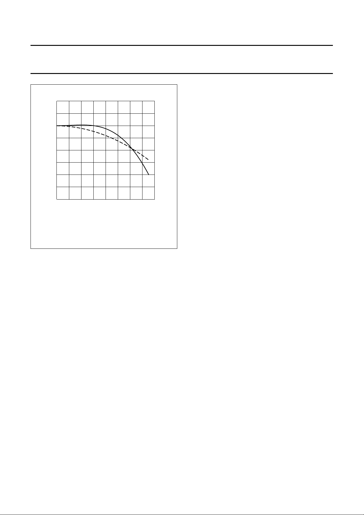
024
(1) SCBW = 1.
(2) SCBW = 0.
(1) (2)
6 8 10 12 14
Fig.5 Chrominance transfer characteristic 1.
1997 Jan 06 7
f (MHz)
Philips Semiconductors Preliminary specification
Digital Video Encoder (ConDENC) SAA7120; SAA7121
signal TTXRQ a single teletext bit has to be provided after
handbook, halfpage
G
(dB)
2
v
0
−2
−4
MBE735
(1)
(2)
a programmable delay at input pin.
Phase variant interpolation is achieved on this bitstream in
the internal teletext encoder, providing sufficient small
phase jitter on the output text lines.
TTXRQ provides a fully programmable request signal to
the teletext source, indicating the insertion period of
bitstream at lines selectable independently for both fields.
The internal insertion window for text is set to 360
(PAL-WST), 296 (NTSC-WST) or 288 (NABTS) teletext
bits including clock run-in bits. For protocol and timing
see Fig.7.
C
LOSED CAPTION ENCODER
−6
0 0.4 0.8 1.6
(1) SCBW = 1.
(2) SCBW = 0.
1.2
f (MHz)
Fig.6 Chrominance transfer characteristic 2.
In order to enable easy analog post-filtering, luminance is
interpolated from 13.5 MHz data rate to 27 MHz data rate,
providing luminance in 10-bit resolution. This filter is also
used to define smoothed transients for synchronization
pulses and blanking period. For transfer characteristic of
the luminance interpolation filter see Figs 3 and 4.
Chrominance is modified in gain (programmable
separately for U and V), standard dependent burst is
inserted, before baseband colour signals are interpolated
from 6.75 MHz data rate to 27 MHz data rate. One of the
interpolation stages can be bypassed, thus providing a
higher colour bandwidth, which can be made use of for
Y and C output. For transfer characteristics of the
chrominance interpolation filter see Figs 5 and 6.
The amplitude, beginning and ending of inserted burst is
programmable in a certain range, suitable for standard
signals and for special effects. Behind the succeeding
quadrature modulator, colour in 10-bit resolution is
provided on subcarrier.
The numeric ratio between Y and C outputs is in
accordance with set standards.
Using this circuit, data in accordance with the specification
of closed caption or extended data service, delivered by
the control interface, can be encoded (Line 21).
Two dedicated pairs of bytes (two bytes per field), each
pair preceded by run-in clocks and framing code, are
possible.
The actual line number where data is to be encoded in, can
be modified in a certain range.
Data clock frequency is in accordance with definition for
NTSC-M standard 32 times horizontal line frequency.
Data LOW at the output of the DACs corresponds to 0 IRE,
data HIGH at the output of the DACs corresponds to
approximately 50 IRE.
It is also possible to encode Closed Caption Data for 50 Hz
field frequencies at 32 times horizontal line frequency.
NTI-TAPING (SAA7120 ONLY)
A
For more information contact your nearest Philips
Semiconductors sales office.
Data manager
In the data manager, real time arbitration on the data
stream to be encoded is performed.
A pre-defined colour look-up table located in this block can
be read out in a pre-defined sequence (8 steps per active
video line), achieving a colour bar test pattern generator
without the need for an external data source. The colour
bar function is under software control only.
T
ELETEXT INSERTION AND ENCODING
Pin TTX receives a WST- or NABTS-Teletext bitstream
sampled at the LLC clock. At each rising edge of output
1997 Jan 06 8
Output interface/DACs
In the output interface encoded Y and C signals are
converted from digital to analog in 10-bit resolution.

Philips Semiconductors Preliminary specification
Digital Video Encoder (ConDENC) SAA7120; SAA7121
Y and C signals are also combined to a 10-bit CVBS
signal.
The CVBS output occurs with the same processing delay
as the Y and C outputs. Absolute amplitude at the input of
the DAC for CVBS is reduced by15⁄16 with respect to
Y and C DACs to make maximum use of conversion
ranges.
Outputs of the DACs can be set together in two groups via
software control to minimum output voltage for either
purpose.
Synchronization
Synchronization of the ConDENC is able to operate in two
modes; slave mode and master mode.
In the slave mode, the circuit accepts synchronization
pulses at the bidirectional RCV1 port. The timing and
trigger behaviour related to RCV1 can be influenced by
programming the polarity and the on-chip delay of RCV1.
Active slope of RCV1 defines the vertical phase and
optionally the odd/even and colour frame phase to be
initialized, it can be also used to set the horizontal phase.
If the horizontal phase is not to be influenced by RCV1, a
horizontal synchronization pulse needs to be supplied at
the pin RCV2. Timing and trigger behaviour can also be
influenced by RCV2.
If there are missing pulses at RCV1 and/or RCV2, the time
base of ConDENC runs free, thus an arbitrary number of
synchronization slopes may be absent, but no additional
pulses (with the incorrect phase) must occur.
If the vertical and horizontal phase is derived from RCV1,
RCV2 can be used for horizontal or composite blanking
input or output.
Alternatively, the device can be triggered by auxiliary
codes in a
“CCIR 656”
data stream at the MP port.
On the RCV2 port, the device can provide a horizontal
synchronization pulse with programmable start and stop
phase; this pulse can be inhibited in the vertical blanking
period to build up, for example, a composite blanking
signal.
The polarity of both RCV1 and RCV2 is selectable by
software control.
The length of a field and the start and end of its active part
can be programmed. The active part of a field always
starts at the beginning of a line.
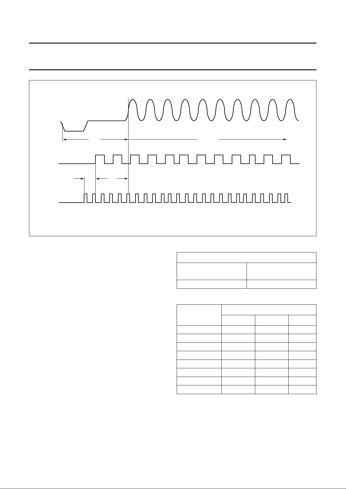
Teletext timing
The teletext timing is shown in Fig.7. tFD is the time needed
to interpolate input data TTX and inserting it into the
CVBS and Y output signal, such that it appears at
t
= 10.2 µs (PAL) or t
TTX
= 10.5 µs (NTSC) after the
TTX
leading edge of the horizontal synchronization pulse.
Time tPD is the pipeline delay time introduced by the
source that is gated by TTXRQ in order to deliver TTX
data. This delay is programmable by register TTXHD.
For every active HIGH-state at output pin TTXRQ, a new
teletext bit must be provided by the source.
Since the beginning of the pulses representing the TTXRQ
signal and the delay between the rising edge of TTXRQ
and valid teletext input data are fully programmable
(TTXHS and TTXHD), the TTX data is always inserted at
the correct position after the leading edge of outgoing
horizontal synchronization pulse.
Time t
is the internally used insertion window for
TTXWin
TTX data; it has a constant length that allows insertion of
360 teletext bits at a text data rate of 6.9375 Mbits/s
(PAL), 296 teletext bits at a text data rate of 5.7272 Mbits/s
(World Standard TTX) or 288 teletext bits at a text data
rate of 5.7272 Mbits/s (NABTS). The insertion window is
not opened if the control bit TTXEN is logic 0.
In the master mode, the time base of the circuit
continuously runs free. On the RCV1 port, the device can
output:
• A Vertical Synchronisation signal (VS) with 3 or 2.5 lines
duration, or
• An ODD/EVEN signal which is LOW in odd fields, or
• A field sequence signal (FSEQ) which is HIGH in the first
of 4 or 8 fields respectively.
1997 Jan 06 9
Using appropriate programming, all suitable lines of the
odd field (TTXOVS and TTXOVE) plus all suitable lines of
the even field (TTXEVS and TTXEVE) can be used for
teletext insertion.
Philips Semiconductors Preliminary specification
Digital Video Encoder (ConDENC) SAA7120; SAA7121
handbook, full pagewidth
CVBS/Y
t
TTX
textbit #: 1 2 3 4 5 6 7 8 9 10 11 12 13 14 15 16 17 18 19 20 21 22 23 24
TTX
TTXRQ
t
PD
t
FD
Fig.7 Teletext timing.
Analog output voltages
The analog output voltages are dependent on the
open-loop voltage of the operational amplifiers for
full-scale conversion (typical value 1.35 V), the internal
series resistor (typical value 2 Ω), the external series
resistor and the external load impedance.
The digital output signals in front of the DACs under
nominal conditions occupy different conversion ranges, as
indicated in Table 1 for a
100
⁄
colour bar signal.
100
Values for the external series resistors result in a 75 Ω
load.
Input levels and formats
The ConDENC expects digital Y, Cb, Cr data with levels
(digital codes) in accordance with
“CCIR 601”
(see
Tables 2 and 3).
For C and CVBS outputs, deviating amplitudes of the
colour difference signals can be compensated by
independent gain control setting, while gain for luminance
is set to predefined values, distinguishable for 7.5 IRE
set-up or without set-up.
t
TTXWin
MBH788
Table 1 Digital output signals conversion range
CONVERSION RANGE (peak-to-peak) (digits)
CVBS, SYNC
TIP-TO-PEAK CARRIER
Y (VBS) SYNC
TIP-TO-WHITE
1016 881
Table 2
“CCIR 601”
signal component levels
SIGNALS
COLOUR
YCbCr
White 235 128 128
Yellow 210 16 146
Cyan 170 166 16
Green 145 54 34
Magenta 106 202 222
Red 81 90 240
Blue 41 240 110
Black 16 128 128
Reference levels are measured with a colour bar,
100% white, 100% amplitude and 100% saturation.
1997 Jan 06 10
 Loading...