

Philips SAA5296AH, SAA5296APS, SAA5291AH, SAA5291APS, SAA5291H Datasheet
...
INTEGRATED CIRCUITS
DATA SH EET
SAA5x9x family
Economy teletext and TV
microcontrollers
Preliminary specification
File under Integrated Circuits, IC02
1997 Jul 07

Philips Semiconductors Preliminary specification
Economy teletext and TV microcontrollers SAA5x9x family
CONTENTS
1 FEATURES
1.1 General
1.2 Microcontroller
1.3 Teletext acquisition
1.4 Teletext Display
1.5 Additional features of SAA529xA devices
1.6 Additional features of SAA549x devices
2 GENERAL DESCRIPTION
3 ORDERING INFORMATION
4 QUICK REFERENCE DATA
5 BLOCK DIAGRAM
6 PINNING INFORMATION
6.1 Pinning
6.2 Pin description
7 FUNCTIONAL DESCRIPTION
7.1 Microcontroller
7.2 80C51 Features not supported
7.3 Additional features
7.4 Microcontroller interfacing
8 TELETEXT DECODER
8.1 Data slicer
8.2 Acquisition timing
8.3 Teletext acquisition
8.4 Rolling headers and time
8.5 Error checking
8.6 Memory organisation of SAA5296/7,
SAA5296/7A and SAA5496/7
8.7 Inventory page
8.8 Memory Organisation of SAA5291, SAA5291A
and SAA5491
8.9 Packet 26 processing
8.10 VPS
8.11 Wide Screen Signalling (SAA529xA and
SAA549x only)
8.12 525-line world system teletext
8.13 Fastext detection
8.14 Page clearing
8.15 Full channel operation
8.16 Independent data services (SAA5291,
SAA5291A, SAA5491 only)
9 THE DISPLAY
9.1 Introduction
9.2 Character matrix
9.3 East/West selection
9.4 National option characters
9.5 The twist attribute
9.6 On Screen Display symbols
9.7 Language group identification
9.8 525-line operation
9.9 On Screen Display characters
9.10 Control characters
9.11 Quadruple width display (SAA549x)
9.12 Page attributes
9.13 Display modes
9.14 On Screen Display boxes
9.15 Screen colour
9.16 Redefinable Colours (SAA549x)
9.17 Cursor
9.18 Other display features
9.19 Display timing
9.20 Horizontal timing
9.21 Vertical timing
9.22 Display position
9.23 Clock generator
10 CHARACTER SETS
10.1 Pan-European
10.2 Russian
10.3 Greek/Turkish
10.4 Arabic/English/French
10.5 Thai
10.6 Arabic/Hebrew
11 LIMITING VALUES
12 CHARACTERISTICS
13 CHARACTERISTICS FOR THE I2C-BUS
INTERFACE
14 QUALITY SPECIFICATIONS
15 APPLICATION INFORMATION
16 EMC GUIDELINES
17 PACKAGE OUTLINES
18 SOLDERING
18.1 Introduction
18.2 SDIP
18.3 QFP
19 DEFINITIONS
20 LIFE SUPPORT APPLICATIONS
21 PURCHASE OF PHILIPS I2C COMPONENTS
1997 Jul 07 2

Philips Semiconductors Preliminary specification
Economy teletext and TV microcontrollers SAA5x9x family
1 FEATURES
1.1 General
• Single chip microcontroller with integrated teletext
decoder
• Single +5 V power supply
• Single crystal oscillator for teletext decoder, display and
microcontroller
• Teletext function can be powered-down independently
of microcontroller function for reduced power
consumption in stand-by
• Pin compatibility throughout family.
1.2 Microcontroller
• 80C51 microcontroller core
• 16/32/64 kbyte mask programmed ROM
• 256/768/1280 bytes of microcontroller RAM
• Eight 6-bit Pulse Width Modulator (PWM) outputs for
control of TV analog signals
• One 14-bit PWM for Voltage Synthesis Tuner control
• Four 8-bit Analog-to-Digital converters
• 2 high current open-drain outputs for directly driving
LED’s etc.
2
• I
C-bus interface
• External ROM and RAM capability on QFP80 package
version.
1.4 Teletext Display
• 525-line and 625-line display
• 12 × 10 character matrix
• Double height, width and size On-Screen Display (OSD)
• Definable border colour
• Enhanced display features including meshing and
shadowing
• 260 characters in mask programmed ROM
• Automatic FRAME output control with manual override
• RGB push pull output to standard decoder ICs
• Stable display via slave synchronisation to Horizontal
Sync and Vertical Sync.
1.5 Additional features of SAA529xA devices
• Wide Screen Signalling (WSS) bit decoding (line 23).
1.6 Additional features of SAA549x devices
• Wide Screen Signalling bit decoding (line 23)
• Quad width OSD capability
• 32 additional OSD characters in mask programmed
ROM
• 8 foreground and 8 background colours definable from a
palette of 64.
2 GENERAL DESCRIPTION
1.3 Teletext acquisition
• 1 page and 10 page Teletext version
• Acquisition of 525-line and 625-line World System
Teletext, with automatic selection
• Acquisition and decoding of VPS data (PDC system A)
• Page clearing in under 64 µs (1 TV line)
• Separate storage of extension packets
(SAA5296/7, SAA5296/7A and SAA5496/7)
• Inventory of transmitted Teletext pages stored in the
Transmitted Page Table (TPT) and Subtitle Page Table
(SPT) (SAA5296/7, SAA5296/7A and SAA5496/7)
• Automatic detection of FASTEXT transmission
• Real-time packet 26 engine for processing accented
(and other) characters
• Comprehensive Teletext language coverage
• Video signal quality detector.
1997 Jul 07 3
The SAA529x, SAA529xA and SAA549x family of
microcontrollers are a derivative of the Philips’
industry-standard 80C51 microcontroller and are intended
for use as the central control mechanism in a television
receiver. They provide control functions for the television
system and include an integrated teletext function.
The teletext hardware has the capability of decoding and
displaying both 525-line and 625-line World System
Teletext. The same display hardware is used both for
Teletext and On-Screen Display, which means that the
display features give greater flexibility to differentiate the
TV set.
The family offers both 1 page and 10 page Teletext
capability, in a range of ROM sizes. Increasing display
capability is offered from the SAA5290 to the SAA5497.
Philips Semiconductors Preliminary specification
Economy teletext and TV microcontrollers SAA5x9x family
3 ORDERING INFORMATION
TYPE NUMBER
(1)
PACKAGE
NAME DESCRIPTION VERSION
SAA5290PS/nnn SDIP52 plastic shrink dual in-line package; 52 leads
(600 mil)
SAA5291PS/nnn
SAA5291APS/nnn
SAA5296PS/nnn
SAA5296APS/nnn
SDIP52
plastic shrink dual in-line package; 52 leads
(600 mil)
SAA5491PS/nnn
SAA5496PS/nnn
SAA5291H/nnn
SAA5291AH/nnn
SAA5296H/nnn
SAA5296AH/nnn
QFP80
plastic quad flat package; 80 leads (lead length
1.95 mm); body 14 × 20 × 2.8 mm
SAA5491H/nnn
SAA5496H/nnn
SAA5297PS/nnn
SDIP52
plastic shrink dual in-line package; 52 leads
(600 mil)
SAA5497PS/nnn
SAA5297H/nnn
QFP80
plastic quad flat package; 80 leads (lead length
1.95 mm); body 14 × 20 × 2.8 mm
SAA5497H/nnn
PROGRAM
MEMORY (ROM)
SOT247-1 16 kbytes
SOT247-1 32 kbytes
SOT318-2 32 kbytes and external
SOT247-1 64 kbytesSAA5297APS/nnn
SOT318-2 64 kbytes or externalSAA5297AH/nnn
Note
1. ‘nnn’ is a three-digit number uniquely referencing the microcontroller program mask and OSD mask.
4 QUICK REFERENCE DATA
SYMBOL PARAMETER MIN. TYP. MAX. UNIT
V
V
V
f
xtal
T
I
DDM
DDA
DDM
DDT
amb
supply voltages 4.5 5.0 5.5 V
crystal frequency − 12 − MHz
operating ambient temperature −20 − +70 °C
microcontroller supply current − 20 35 mA
SAA5290, SAA5291, SAA5291A and SAA5491
I
DDA
I
DDT
analog supply current − 35 50 mA
teletext supply current − 40 65 mA
SAA5296, SAA5296A, SAA5297, SAA5297A, SAA5496 and SAA5497
I
DDA
I
DDT
analog supply current − 35 50 mA
teletext supply current − 50 80 mA
1997 Jul 07 4
Philips Semiconductors Preliminary specification
Economy teletext and TV microcontrollers SAA5x9x family
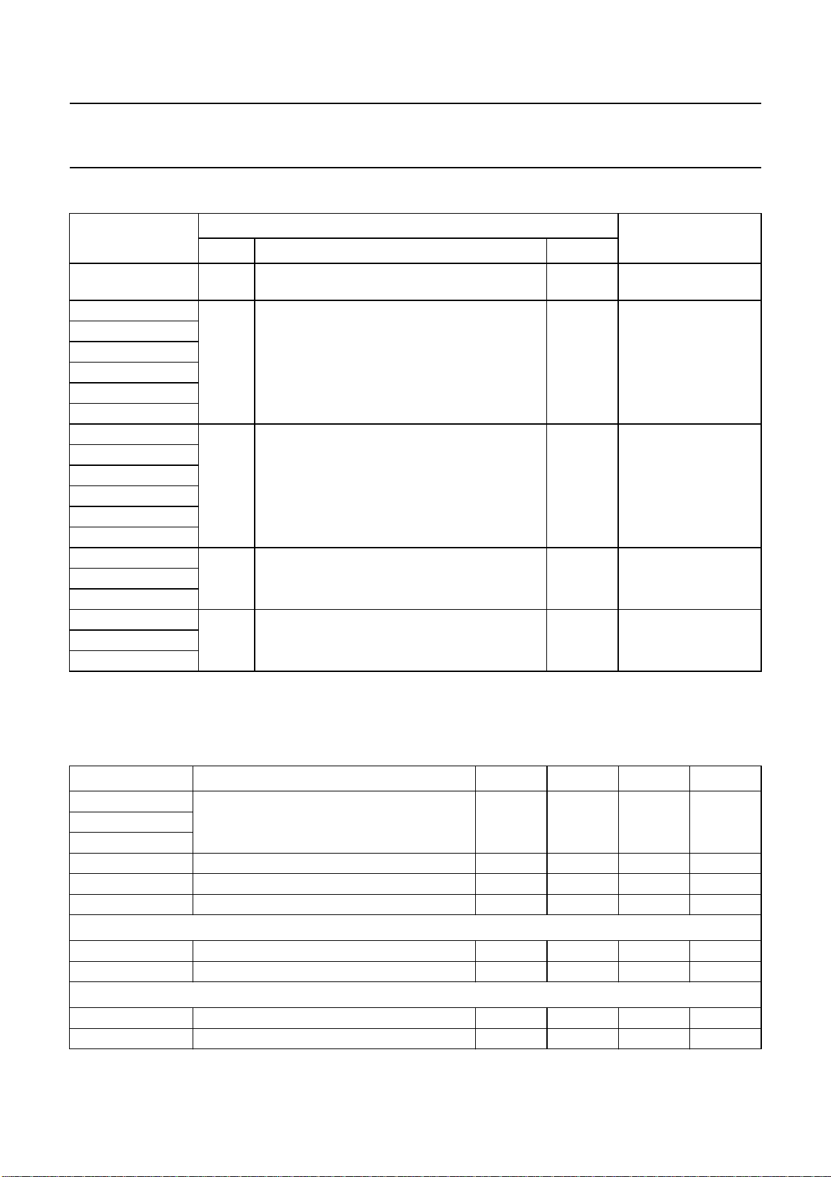
5 BLOCK DIAGRAM
handbook, full pagewidth
CVBS0,
CVBS1
XTALIN
XTALOUT
OSCGND
RESET
OSCILLATOR
8051
MICRO-
CONTROLLER
int
SAA5x9x
data
address
BLACK IREF
DATA SLICER
ACQUISITION
TIMING
512 × 8
AUX RAM
2
I
C-BUS
INTERFACE
PORT 1 PORT 0 PORT 3 PORT 2
TIMER/
CTRS
V
DDAVDDMVDDTVSSAVSSD
TELETEXT
ACQUISITION
32K × 8
ROM
256 × 8
RAM
ADC
DISPLAY
PAGE
RAM
DISPLAY
TIMING
TEXT
INTERFACE
PWM
R, G, B,
VDS,
COR
VSYNC
HSYNC
FRAME
MGK462
P1.0 to P1.7 P0.0 to P0.7 P3.0 to P3.7 P2.0 to P2.7
Fig.1 Block diagram.
1997 Jul 07 5
Philips Semiconductors Preliminary specification
Economy teletext and TV microcontrollers SAA5x9x family
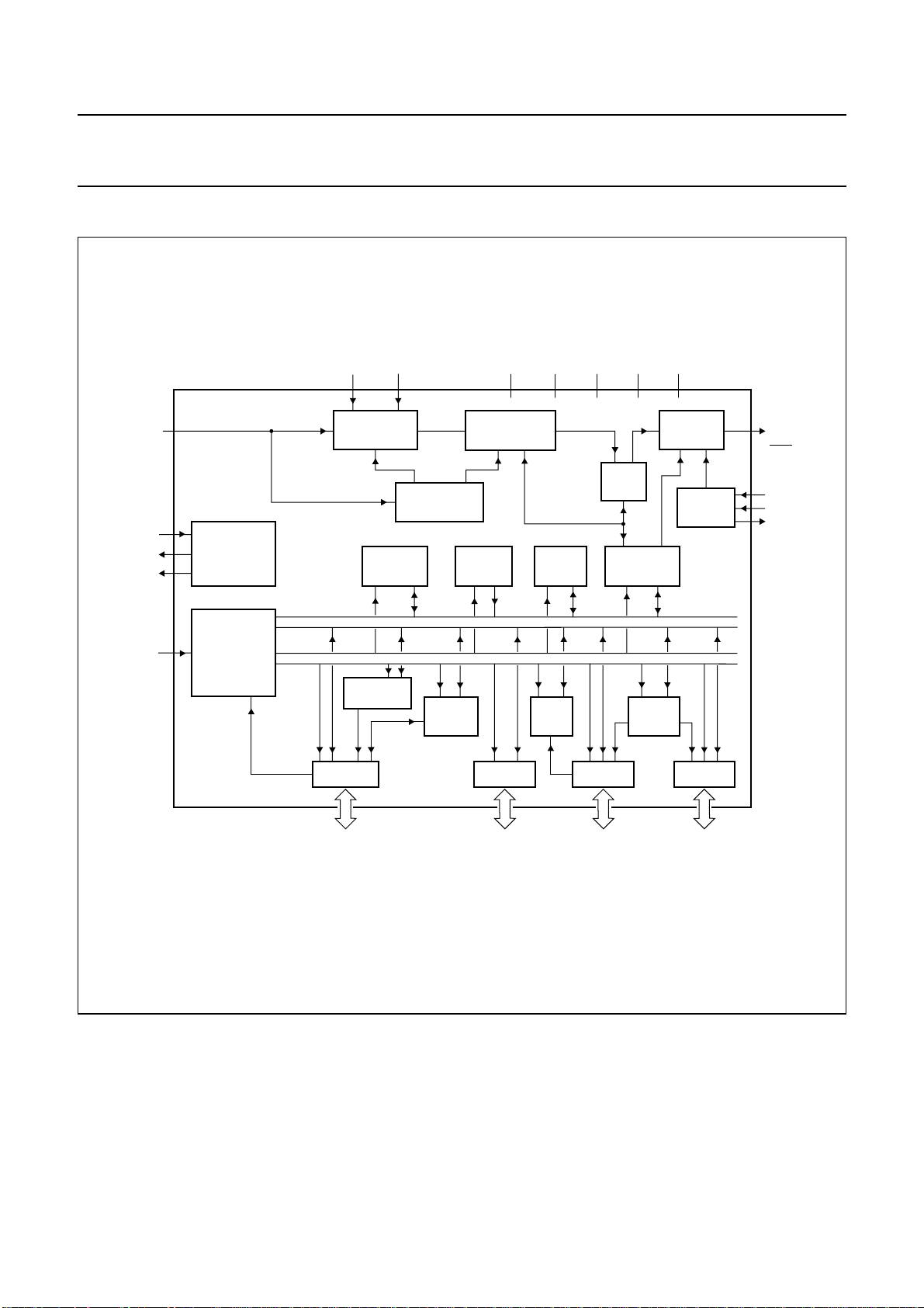
6 PINNING INFORMATION
6.1 Pinning
handbook, halfpage
P2.0/TPWM
P2.1/PWM0
P2.2/PWM1
P2.3/PWM2
P2.4/PWM3
P2.5/PWM4
P2.6/PWM5
P2.7/PWM6
P3.0/ADC0
P3.1/ADC1
P3.2/ADC2
P3.3/ADC3
1
2
3
4
5
6
7
8
9
10
11
12
V
13
SSD
P0.0
P0.1
P0.2
P0.3
14
15
16
17
SAA5x9x
52
51
50
49
48
47
46
45
44
43
42
41
40
39
38
37
36
P1.5
P1.4
P1.7/SDA
P1.6/SCL
P1.3/T1
P1.2/INT0
P1.1/T0
P1.0/INT1
V
DDM
RESET
XTALOUT
XTALIN
OSCGND
V
DDT
V
DDA
VSYNC
HSYNC
18
P0.4
19
P0.5
20
P0.6
21
P0.7
V
22
SSA
IREF
23
24
25
26
CVBS0
CVBS1
BLACK
Fig.2 Pin configuration (SDIP52).
1997 Jul 07 6
MGK461
35
34
33
32
31
30
29
28
27
VDS
R
G
B
RGBREF
P3.4/PWM7
COR
V
SSD
FRAME
Philips Semiconductors Preliminary specification
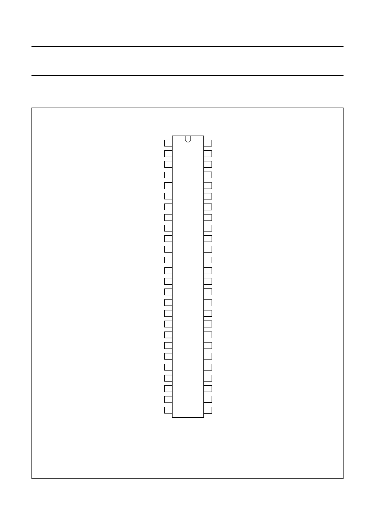
Economy teletext and TV microcontrollers SAA5x9x family
handbook, full pagewidth
P2.6/PWM5
P2.7/PWM6
P3.0/ADC0
P3.1/ADC1
P3.2/ADC2
P3.3/ADC3
P2.5/PWM4
P2.4/PWM3
n.c.
RD
WR
V
SSD
EA
P0.0
P0.1
P0.2
PSEN
ALE
REF−
P0.3
P0.4
P3.7
n.c.
P0.5
1
2
3
4
5
6
7
8
9
10
11
12
13
14
15
16
17
18
19
20
21
22
23
24
P2.3/PWM2
P2.2/PWM1
80
79
25
26
P0.6
P0.7
P2.1/PWM0
P2.0/TPWM
78
77
27
28
SSA
V
CVBS0
AD7
76
29
CVBS1
AD6
75
30
BLACK
AD5
AD4
74
73
SAA5x9x
31
32
A15
IREF
AD3
72
33
A14
AD2
71
34
A13
AD1
70
35
A12
AD0
69
36
V
FRAME
P1.5
68
37
SSD
P1.4
67
38
COR
P1.7/SDA
P1.6/SCL
66
65
39
40
B
RGBREF
P1.1/T0
64
63
P1.0/INT1
62
V
P1.3/T1
61
60
P1.2/INT0
59
RESET
58
XTALOUT
57
XTALIN
56
OSCGND
55
A8
54
A9
53
A10
52
A11
51
V
50
REF+
49
V
48
P3.6
47
VSYNC
46
P3.5
45
HSYNC
44
P3.4/PWM7
43
VDS
42
R
41
G
MGL157
DDM
DDT
DDA
Fig.3 Pin configuration (QFP80).
1997 Jul 07 7
Philips Semiconductors Preliminary specification
Economy teletext and TV microcontrollers SAA5x9x family
6.2 Pin description
Table 1 SDIP52 and QFP80 packages
SYMBOL
DESCRIPTION
SDIP52 QFP80
P2.0/TPWM 1 77 Port 2: 8-bit open-drain bidirectional port with alternative functions.
PIN
P2.1/PWM0 2 78
P2.2/PWM1 3 79
P2.0/TPWM is the output for the 14-bit high precision PWM.
P2.1/PWM0 to P2.7/PWM6 are the outputs for the 6-bit PWMs 0 to 6.
P2.3/PWM2 4 80
P2.4/PWM3 5 9
P2.5/PWM4 6 8
P2.6/PWM5 7 1
P2.7/PWM6 8 2
P3.0/ADC0 9 3 Port 3: 8-bit open-drain bidirectional port with alternative functions.
P3.1/ADC1 10 5
P3.2/ADC2 11 6
P3.0/ADC0 to P3.3/ADC3 are the inputs for the software ADC facility.
P3.4/PWM7 is the output for the 6-bit PWM7.
P3.3/ADC3 12 7
P3.4/PWM7 30 44
P3.5 − 46
P3.6 − 48
P3.7 − 22
V
SSD
13 12 Digital ground.
P0.0 14 14 Port 0: 8-bit open-drain bidirectional port.
P0.1 15 15
P0.5 and P0.6 have 10 mA current sinking capability for direct drive of LEDs.
P0.2 16 16
P0.3 17 20
P0.4 18 21
P0.5 19 24
P0.6 20 25
P0.7 21 26
V
SSA
22 27 Analog ground.
CVBS0 23 28 Composite video inputs; a positive-going 1 V (peak-to-peak) input is required,
CVBS1 24 29
BLACK 25 30 Video black level storage input: this pin should be connected to V
connected via a 100 nF capacitor.
SSA
via a
100 nF capacitor.
IREF 26 31 Reference current input for analog circuits, connected to V
via a 27 kΩ
SSA
resistor.
FRAME 27 36 De-interlace output synchronised with the VSYNC pulse to produce a
non-interlaced display by adjustment of the vertical deflection circuits.
V
SSD
28 37 Internally connected; this pin should be connected to digital ground.
COR 29 38 Open-drain, active LOW output which allows selective contrast reduction of
the TV picture to enhance a mixed mode display.
1997 Jul 07 8
Philips Semiconductors Preliminary specification
Economy teletext and TV microcontrollers SAA5x9x family
SYMBOL
DESCRIPTION
SDIP52 QFP80
LRGBREF 31 39 DC input voltage to define the output HIGH level on the RGB pins.
B 32 40 Pixel rate output of the BLUE colour information.
G 33 41 Pixel rate output of the GREEN colour information.
R 34 42 Pixel rate output of the RED colour information.
VDS 35 43 Video/data switch push-pull output for dot rate fast blanking.
HSYNC 36 45 Schmitt trigger input for a TTL level version of the horizontal sync pulse; the
polarity of this pulse is programmable by register bit TXT1.H POLARITY.
VSYNC 37 47 Schmitt trigger input for a TTL level version of the vertical sync pulse;
the polarity of this pulse is programmable by register bit TXT1.V POLARITY.
PIN
V
V
DDA
DDT
38 49 +5 V analog power supply.
39 51 +5 V teletext power supply.
OSCGND 40 56 Crystal oscillator ground.
XTALIN 41 57 12 MHz crystal oscillator input.
XTALOUT 42 58 12 MHz crystal oscillator output.
RESET 43 59 If the reset input is HIGH for at least 3 machine cycles (36 oscillator periods)
while the oscillator is running, the device is reset; this pin should be
via a 2.2 µF capacitor.
DDM
V
DDM
connected to V
44 62 +5 V microcontroller power supply.
P1.0/INT1 45 63 Port 1: 8-bit open-drain bidirectional port with alternate functions.
P1.1/T0 46 64
P1.2/INT0 47 60
P1.3/INT1 48 61
P1.6/SCL 49 65
P1.0/INT1 is external interrupt 1 which can be triggered on the rising and
falling edge of the pulse.
P1.1/T0 is the counter/timer 0.
P1.2/INT0 is external interrupt 0.
P1.7/SDA 50 66
P1.4 51 67
P1.5 52 68
P1.3/T1 is the counter/timer 1.
P1.6/SCL is the serial clock input for the I
2
C-bus.
P1.7/SDA is the serial data port for the I2C-bus.
REF+ − 50 Positive reference voltage for software driven ADC.
REF−−19 Negative reference voltage for software driven ADC.
RD − 10 Read control signal to external Data Memory.
WR − 11 Write control signal to external Data Memory.
PSEN − 17 Enable signal for external Program Memory.
ALE − 18 External latch enable signal; active HIGH.
EA − 13 Control signal used to select external (LOW) or internal (HIGH) Program
Memory.
AD0 to AD7 − 69 to 76 Address lines A0 to A7 multiplexed with data lines D0 to D7.
A8 to A15 − 55 to 52,
Address lines A8 to A15.
35 to 32
1997 Jul 07 9
Philips Semiconductors Preliminary specification
Economy teletext and TV microcontrollers SAA5x9x family
7 FUNCTIONAL DESCRIPTION
7.1 Microcontroller
The functionality of the microcontroller used in this family
is described here with reference to the industry-standard
80C51 microcontroller. A full description of its functionality
can be found in the
Data Handbook IC20”
“80C51-Based 8-Bit Microcontrollers;
. Using the 80C51 as a reference,
the changes made to this family fall into two categories:
• Features not supported by the SAA529x, SAA529xA or
SAA549x devices
• Features found on the SAA529x, SAA529xA or
SAA549x devices but not supported by the 80C51.
7.2 80C51 features not supported
7.2.1 INTERRUPT PRIORITY
The IP SFR is not implemented and all interrupts are
treated with the same priority level. The normal
prioritisation of interrupts is maintained within the level.
Table 2 Interrupts and vectors address
INTERRUPT SOURCE VECTOR ADDRESS
Reset 000H
External INT0 003H
Timer 0 00BH
External INT1 013H
Timer 1 01BH
2
Byte I
C-bus 02BH
2
Bit I
C-bus; note 1 053H
Note
1. SAA5290, SAA5291, SAA5291A and SAA5491 only.
7.2.2 O
FF-CHIP MEMORY
The SDIP52 version does not support the use of off-chip
program memory or off-chip data memory.
7.2.3 I
DLE AND POWER-DOWN MODES
As Idle and Power-down modes are not supported, their
respective bits in PCON are not available.
7.2.4 UART F
UNCTION
The 80C51 UART is not available. As a consequence the
SCON and SBUF SFRs are removed and the ES bit in the
IE SFR is unavailable.
7.3 Additional features
The following features are provided in addition to the
standard 80C51 features.
7.3.1 I
NTERRUPTS
The external INT1 interrupt is modified to generate an
interrupt on both the rising and falling edges of the INT1
pin, when EX1 bit is set. This facility allows for software
pulse width measurement for handling of a remote control.
7.3.2 B
IT LEVEL I
2
C-BUS INTERFACE
For reasons of compatibility with SAA5290, the SAA5291,
SAA5291A and SAA5491 contain a bit level serial I/O
which supports the I2C-bus. P1.6/SCL and P1.7/SDA are
the serial I/O pins. These two pins meet the I2C-bus
specification
specifications)”
“The I2C-bus and how to use it (including
concerning the input levels and output
drive capability. Consequently, these two pins have an
open-drain output configuration. All the four following
modes of the I2C-bus are supported.
• Master transmitter
• Master receiver
• Slave transmitter
• Slave receiver.
Three SFRs support the function of the bit-level I2C-bus
hardware: S1INT, S1BIT and S1SCS and are enabled by
setting register bit TXT8.I2C SELECT to logic 0.
7.3.3 B
YTE LEVEL I
2
C-BUS INTERFACE
The byte level serial I/O supports the I2C-bus protocol.
P1.6/SCL and P1.7/SDA are the serial I/O pins. These two
pins meet the I2C-bus specification concerning the input
levels and output drive capability. Consequently, these two
pins have an open-drain output configuration.
The byte level I2C-bus serial port is identical to the I2C-bus
serial port on the 8xC552. The operation of the subsystem
is described in detail in the 8xC552 data sheet found in
“80C51-Based 8-Bit Microcontrollers; Data Handbook
IC20”
.
Four SFRs support the function of the byte level I2C-bus
hardware, they are S1CON, S1STA, S1DAT and S1ADR
and are enabled by setting register bit TXT8.I2C SELECT
to logic 1.
7.3.4 LED
SUPPORT
Port pins P0.5 and P0.6 have a 10 mA current sinking
capability to enable LEDs to be driven directly.
1997 Jul 07 10
Philips Semiconductors Preliminary specification
Economy teletext and TV microcontrollers SAA5x9x family
7.3.5 6-BIT PWM DACS
Eight 6-bit DACs are available to allow direct control of analog parts of the television.
Each low resolution 6-bit DAC is controlled by its associated Special Function Register (PWM0 to PWM7). The PWM
outputs are alternative functions of Port 2 and Port 3.4. The PWE bit in the SFR for the port corresponding to the PWM
should be set to logic 1 for correct operation of the PWM, e.g. if PWM0 is to be used, P2.1 should be set to logic 1 setting
the port pin to high-impedance.
7.3.5.1 Pulse Width Modulator Registers (PWM0 to PWM7)
Table 3 Pulse Width Modulator Registers (see Table 10 for addresses)
76543210
PWE − PV5 PV4 PV3 PV2 PV1 PV0
Table 4 Description of PWMn bits (n=0to7)
BIT SYMBOL DESCRIPTION
7 PWE If PWE is set to a logic 1, the corresponding PWM is active and controls its assigned
port pin. If PWE is set to a logic 0, the port pin is controlled by the corresponding bit in
the port SFR.
6 − Not used.
5 PV5 The output of the PWM is a pulse of period 21.33 µs with a pulse HIGH time determined
4 PV4
3 PV3
2 PV2
1 PV1
0 PV0
by the binary value of these 6-bits multiplied by 0.33 µs. PV5 is the most significant bit.
1997 Jul 07 11
Philips Semiconductors Preliminary specification
Economy teletext and TV microcontrollers SAA5x9x family
7.3.6 14-BIT PWM DAC
One 14-bit DAC is available to allow direct control of
analog sections of the television. The 14-bit PWM is
controlled using Special Function Registers TDACL and
TDACH.
The output of the TPWM is a pulse of period 42.66 µs. The
7 most significant bits, TDACH.TD13
(MSB) to TDACH.TD8 and TDACL.TD7, alter the pulse
width between 0 and 42.33 µs, in much the same way as
in the 6-bit PWMs. The 7 least significant bits, TDACL.TD6
to TDACL.TD0 (LSB), extend certain pulses by a further
0.33 µs, e.g. if the 7 least significant bits are given the
value 01H, then 1 in 128 cycles is extended. If the 7 least
significant bits are given the value 02H, then
2 in 128 cycles is extended, and so forth.
The TPWM will not start to output a new value until after
writing a value to TDACH. Therefore, if the value is to be
changed, TDACL should be written to before TDACH.
7.3.6.1 TPWM High Byte Register (TDACH)
Table 5 TPWM High Byte Register (SFR address D3H)
76543210
PWE − TD13 TD12 TD11 TD10 TD9 TD8
Table 6 Description of TDACH bits
BIT SYMBOL DESCRIPTION
7 PWE If PWE is set to a logic 1, the TPWM is active and controls port line P2.0. If PWE is set
to a logic 0, the port pin is controlled by the corresponding bit in the port SFR.
6 − Not used.
5 TD13 These 6-bits along with bit TD7 in the TDACL register control the pulse width period.
4 TD12
3 TD11
2 TD10
1 TD9
0 TD8
TD13 is the most significant bit.
7.3.6.2 TPWM Low Byte Register (TDACL)
Table 7 TPWM Low Byte Register (SFR address D2H)
76543210
TD7 TD6 TD5 TD4 TD3 TD2 TD1 TD0
Table 8 Description of TDACL bits
BIT SYMBOL DESCRIPTION
7 TD7 This bit is used with bits TD13 to TD8 in the TDACH register to control the pulse width
period.
6 to 0 TD6 to TD0 These 7-bits extend certain pulses by a further 0.33 µs.
1997 Jul 07 12
Philips Semiconductors Preliminary specification
Economy teletext and TV microcontrollers SAA5x9x family
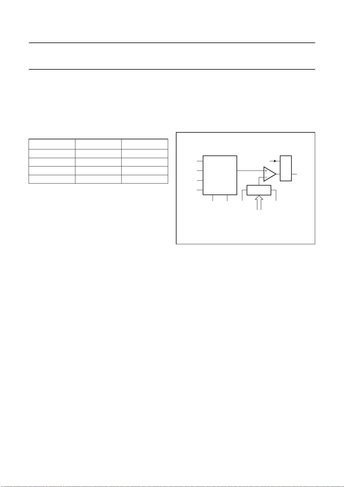
7.3.7 SOFTWARE ADC
Up to 4 successive approximation ADCs can be
implemented in software by making use of the on-chip 8-bit
DAC and multiplexed voltage comparator. The software
ADC uses 4 analog inputs which are multiplexed with
P3.0 to P3.3.
Table 9 ADC input channel selection
CH1 CH0 INPUT PIN
0 0 P3.3/ADC3
0 1 P3.0/ADC0
1 0 P3.1/ADC1
1 1 P3.2/ADC2
The control of the ADC is achieved using the Special
Function Registers SAD and SADB.
SAD.CH1 and SAD.CH0 select one of the four inputs to
pass to the comparator. The other comparator input
comes from the DAC, whose value is set by SAD.SAD7
(MSB) to SAD.SAD4 and SADB.SAD3 to SADB.SAD0
(LSB). The setting of the value SAD.SAD7 to SAD.SAD4
must be performed at least 1 instruction cycle before the
setting of SAD.ST to ensure comparison is made using the
correct SAD.SAD7 to SAD.SAD4 value.
The output of the comparator is SAD.VHI, and is valid after
1 instruction cycle following the setting of SAD.ST to a
logic 1.
handbook, halfpage
P3.0
P3.1
MULTIPLEXER
P3.2
P3.3
CH1, CH0
SAD7 to SAD0
ST C1
8-BIT DAC
1D
REF+REF−
VH1
MGL115
Fig.4 SAD block diagram.
1997 Jul 07 13
1997 Jul 07 14
7.4 Microcontroller interfacing
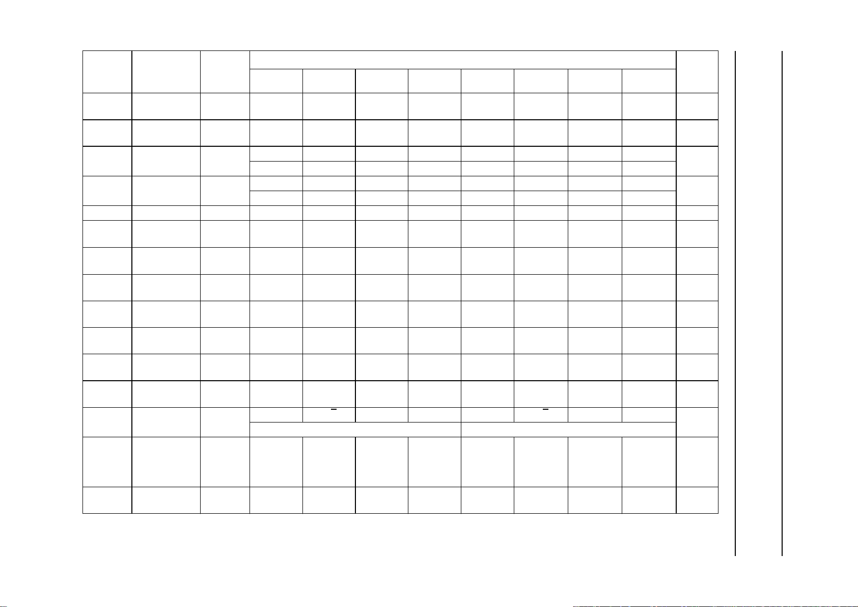
The 80C51 communicates with the peripheral functions using Special Function Registers (SFRs) which are addressed as RAM locations. The registers
in the teletext decoder appear as normal SFRs in the microcontroller memory map, but are written to using an internal serial bus. The SFR map is given
in Table 10.
Philips Semiconductors Preliminary specification
Economy teletext and TV microcontrollers SAA5x9x family
7.4.1 S
PECIAL FUNCTION REGISTER MAP
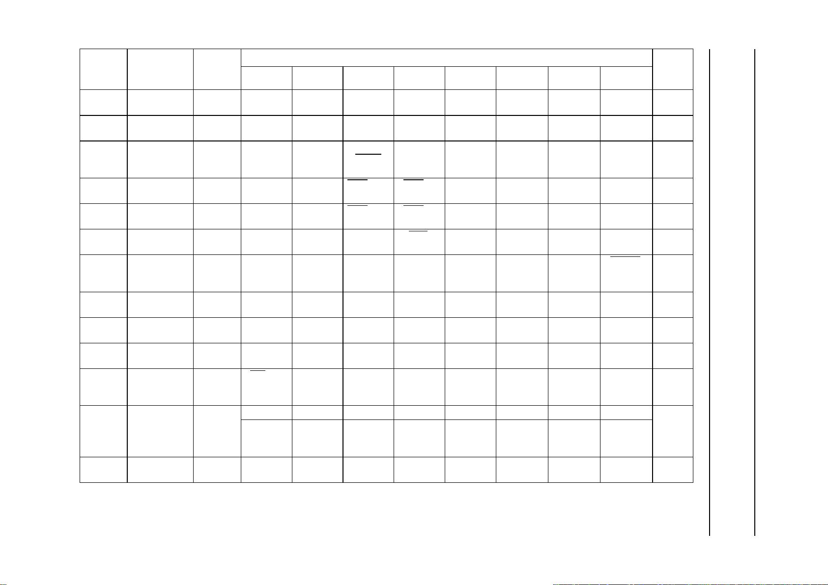
Table 10 Special Function Register map; note 1
DIRECT
SYMBOL NAME
(2)
ACC
Accumulator E0 E7 E6 E5 E4 E3 E2 E1 E0 00
ADDR.
(HEX)
76543210
−−−−−−−−
(2)
B
B register F0 F7 F6 F5 F4 F3 F2 F1 F0 00
−−−−−−−−
DPTR Data Pointer
(2 bytes)
DPH High byte
DPL Low byte
IE
(2)(3)
Interrupt
Enable
P0
(2)
Port 0 80 87 86 85 84 83 82 81 80 FF
83 −−−−−−−−00
82 −−−−−−−−00
A8 AF AE AD AC AB AA A9 A8 00
EA ES1 ES2 * ET1 EX1 ET0 EX0
−−−−−−−−
P1
(2)
Port 1 90 97 96 95 94 93 92 91 90 FF
−−−−−−−−
P2
(2)
Port 2 A0 A7 A6 A5 A4 A3 A2 A1 A0 FF
−−−−−−−−
P3
(2)(3)
Port 3 B0 B7 B6 B5 B4 B3 B2 B1 B0 FF
−−−−−−−−
(3)
PCON
Power Control 87 − ARD − * GF1 GF0 −−10
BIT ADDRESS, SYMBOL OR ALTERNATIVE PORT FUNCTION RESET
VALUE
(HEX)
1997 Jul 07 15
SYMBOL NAME
(2)
PSW
(3)
PWM0
(3)
PWM1
(3)
PWM2
(3)
PWM3
(3)
PWM4
(3)
PWM5
(3)
PWM6
(3)
PWM7
S1ADR
(3)
S1CON
(2)(3)(4)
S1SCS
(2)(3)(5)
S1DAT
(3)(4)
S1INT
(3)(5)
Program
Status Word
Pulse Width
Modulator 0
Pulse Width
Modulator 1
Pulse Width
Modulator 2
Pulse Width
Modulator 3
Pulse Width
Modulator 4
Pulse Width
Modulator 5
Pulse Width
Modulator 6
Pulse Width
Modulator 7
Serial I2C-bus
address
Serial I2C-bus
control
Serial I2C-bus
control
Serial I2C-bus
data
Serial I2C-bus
Interrupt
DIRECT
BIT ADDRESS, SYMBOL OR ALTERNATIVE PORT FUNCTION RESET
ADDR.
(HEX)
76543210
D0 D7 D6 D5 D4 D3 D2 D1 D0 00
CY AC F0 RS1 RS0 OV * P
D5 PWE * PV5 PV4 PV3 PV2 PV1 PV0 40
D6 PWE * PV5 PV4 PV3 PV2 PV1 PV0 40
D7 PWE * PV5 PV4 PV3 PV2 PV1 PV0 40
DC PWE * PV5 PV4 PV3 PV2 PV1 PV0 40
DD PWE * PV5 PV4 PV3 PV2 PV1 PV0 40
DE PWE * PV5 PV4 PV3 PV2 PV1 PV0 40
DF PWE * PV5 PV4 PV3 PV2 PV1 PV0 40
D4 PWE * PV5 PV4 PV3 PV2 PV1 PV0 40
DB ADR6 ADR5 ADR4 ADR3 ADR2 ADR1 ADR0 GC 00
D8 DF DE DD DC DB DA D9 D8
CR2 ENSI STA STO SI AA CR1 CR0 00
D8 DF DE DD DC DB DA D9 D8
SDI SCI CLH BB RBF WBF STR ENS E0
DA DAT7 DAT6 DAT5 DAT4 DAT3 DAT2 DAT1 DAT0 00
DA SI −−−−−−−7F
Philips Semiconductors Preliminary specification
Economy teletext and TV microcontrollers SAA5x9x family
VALUE
(HEX)
1997 Jul 07 16
SYMBOL NAME
S1STA
(3)(4)
S1BIT
(3)(5)
SAD
(2)(3)
SADB
(2)(3)
Serial I2C-bus
status
Serial I2C-bus
data
Software
ADC (MSB)
Software
ADC (LSB)
DIRECT
ADDR.
(HEX)
76543210
D9 STAT4 STAT3 STAT2 STAT1 STAT0 0 0 0 F8
D9 SDO/SDI −−−−−−−7F
E8 EF EE ED EC EB EA E9 E8 00
VHI CH1 CH0 ST SAD7 SAD6 SAD5 SAD4
98 9F 9E 9D 9C 9B 9A 99 98 00
−−−−SAD3 SAD2 SAD1 SAD0
BIT ADDRESS, SYMBOL OR ALTERNATIVE PORT FUNCTION RESET
SP Stack Pointer 81 8F 8E 8D 8C 8B 8A 89 88 07
TCON
(2)
Timer/counter
88 TF1 TR1 TF0 TR0 IE1 IT1 IE0 IT0 00
control
TDACH
TPWM
D3 PWE * TD13 TD12 TD11 TD10 TD9 TD8 40
High byte
TDACL TPWM
D2 TD7 TD6 TD5 TD4 TD3 TD2 TD1 TD0 00
Low byte
TH0 Timer0
8C TH07 TH06 TH05 TH04 TH03 TH02 TH01 TH00 00
High byte
TH1 Timer1
8D TH17 TH16 TH15 TH14 TH13 TH12 TH11 TH10 00
High byte
TL0 Timer 0
8A TL07 TL06 TL05 TL04 TL03 TL02 TL01 TL00 00
Low byte
TL1 Timer 1
8B TL17 TL16 TL15 TL14 TL13 TL12 TL11 TL10 00
Low byte
TMOD Timer/counter
mode
(3)
TXT0
Teletext
Register 0
89 GATE C/
TM1M0GATEC/TM1M000
Timer 1 Timer 0
C0 X24 POSN DISPLAY
X24
AUTO
FRAME
DISABLE
HDR
ROLL
DISPLA Y
ST ATUS
ROW
DISABLE
FRAME
VPS ON INV ON 00
ONL Y
(3)
TXT1
Teletext
Register 1
C1 EXT PKT
OFF
8−BIT ACQ OFF X26
OFF
FULL
FIELD
FIELD
POLARITYHPOLARITYVPOLARITY
Philips Semiconductors Preliminary specification
Economy teletext and TV microcontrollers SAA5x9x family
VALUE
(HEX)
00
1997 Jul 07 17
SYMBOL NAME
(3)
TXT2
(3)
TXT3
(3)
TXT4
(3)
TXT5
(3)
TXT6
(3)
TXT7
(3)
TXT8
(3)
TXT9
(3)
TXT10
(3)
TXT11
(3)
TXT12
TXT13
(2)(3)
(3)
TXT14
Teletext
Register 2
Teletext
Register 3
Teletext
Register 4
Teletext
Register 5
Teletext
Register 6
Teletext
Register 7
T eletext
Register 8
Teletext
Register 9
Teletext
Register 10
Teletext
Register 11
Teletext
Register 12
Teletext
Register 13
Teletext
Register 14
DIRECT
BIT ADDRESS, SYMBOL OR ALTERNATIVE PORT FUNCTION RESET
ADDR.
(HEX)
76543210
C2 * REQ3 REQ2 REQ1 REQ0 SC2 SC1 SC0 00
C3 * * * PRD4 PRD3 PRD2 PRD1 PRD0 00
C4 OSD
BANK
ENABLE
C5 BKGND
OUT
C6 BKGND
OUT
C7 STATUS
ROW TOP
C8 I2C
SELECT
C9 CURSOR
FREEZE
QUAD
WIDTH
ENABLE
BKGND IN COR OUT COR IN TEXT
BKGND IN COR OUT COR IN TEXT
CURSORONREVEAL TOP/
IDS
ENABLE
CLEAR
MEMORY.
EAST/
WEST
* DISABLE
DISABLE
DBL HT
BOTTOM
SP ANISH
B MESH
ENABLE
OUT
OUT
DOUBLE
HEIGHT
PKT26
RECEIVE
D
C MESH
ENABLE
TRANS
ENABLE
TEXT IN PICTURE
ON OUT
TEXT IN PICTURE
ON OUT
BOX ON24BOX ON
1-23
WSS
WSS ON
RECEIVE
D
SHADOW
ENABLE
PICTURE
ON IN
PICTURE
ON IN
BOX ON
0
CVBS0/
CVBS1
A0 R4 R3 R2 R1 R0 00
CA * * C5 C4 C3 C2 C1 C0 00
CB D7 D6 D5 D4 D3 D2 D1 D0 00
CC 625/525
SYNC
ROM
VER R4
ROM
VER R3
ROM
VER R2
ROM
VER R1
ROM VERR0TXT ON VIDEO
SIGNAL
QUALITY
B8 BF BE BD BC BB BA B9 B8 00
VPS
RECEIVE
D
PAGE
CLEARIN
G
525
DISPLAY
525 TEXT 625
TEXT
PKT
8/30
FASTEXT TIB
CD −− −PAGE3 PAGE2 PAGE1 PAGE0 00
Philips Semiconductors Preliminary specification
Economy teletext and TV microcontrollers SAA5x9x family
VALUE
(HEX)
00
03
03
00
00
0XXXX
X00B
1997 Jul 07 18
SYMBOL NAME
(3)
TXT15
Teletext
DIRECT
ADDR.
(HEX)
76543210
CE −−−−BLOCK3 BLOCK2 BLOCK1 BLOCK0 00
BIT ADDRESS, SYMBOL OR ALTERNATIVE PORT FUNCTION RESET
Register 15
(3)
TXT16
Teletext
CF − Y2 Y1 Y0 −−X1 X0 00
Register 16
(3)
TXT17
WSS1
(3)
Teletext
Register 17
WSS
Register 1
B9 − FORCE
ACQ 1
FORCE
ACQ 0
FORCE
625
BA −−−WSS0 to
WSS3
FORCE
WSS3 WSS2 WSS1 WSS0 00
ERROR
WSS2
(3)
WSS
Register 2
BB −−−WSS4 to
WSS7
WSS7 WSS6 WSS5 WSS4 00
ERROR
WSS3
CLUT
(3)
(3)
WSS
Register 3
CLUT
Register
BC WSS11 to
WSS13
ERROR
BD CLUT
ENABLE
WSS13 WSS12 WSS11 WSS8 to
WSS10
ERROR
CLUT
ADDRESS
B1 or − B0 or − G1 or
ENTRY 3
Notes
1. The asterisk (*) indicates these bits are inactive and must be written to logic 0 for future compatibility.
2. SFRs are bit addressable.
3. SFRs are modified or added to the 80C51 SFRs.
4. This register used for Byte Orientated I2C-bus, TXT8.I2C SELECT = 1.
5. This register used for Bit Orientated I2C-bus, TXT8.I2C SELECT = 0.
525
VALUE
(HEX)
SCREEN
COL2
SCREEN
COL1
SCREEN
COL0
WSS10 WSS9 WSS8 00
G0 or
ENTRY 2
R1 or
ENTRY 1
R0 or
ENTRY 0
Philips Semiconductors Preliminary specification
Economy teletext and TV microcontrollers SAA5x9x family
00
00
Philips Semiconductors Preliminary specification
Economy teletext and TV microcontrollers SAA5x9x family
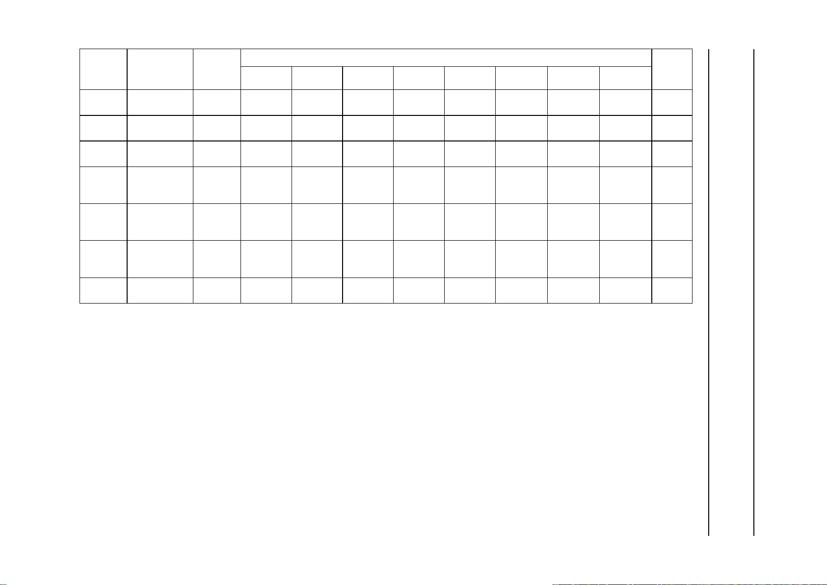
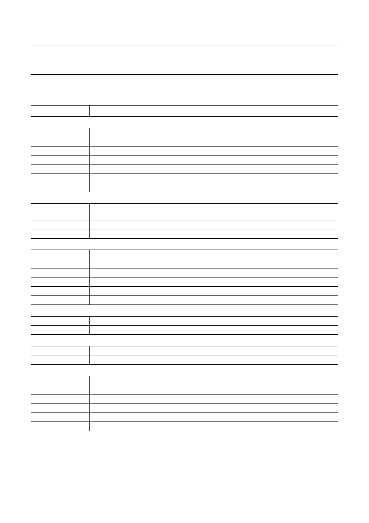
7.4.2 SPECIAL FUNCTION REGISTERS BIT DESCRIPTIONS
Table 11 SFRs bit description
REGISTER FUNCTION
Interrupt Enable Register (IE)
EA disable all interrupts (logic 0) or use individual interrupt enable bits (logic 1)
2
ES1 bit I
ES2 byte I
ET1 enable timer 1 overflow interrupt (logic 1)
EX1 enable external interrupt 1 (logic 1)
ET0 enable timer 0 overflow interrupt (logic 1)
EX0 enable external interrupt 0 (logic 1)
Power Control Register (PCON)
ARD AUX-RAM disable bit. Disables the 512 bytes of internal AUX-RAM (logic 1);
GF1 general purpose flag 1
GF0 general purpose flag 0
C-bus interrupt enable (logic 1)
2
C-bus interrupt enable (logic 1)
all MOVX-instructions access the external data memory
Program Status Word (PSW)
CY carry flag
AC auxiliary carry flag
F0 flag 0
RS1,RS0 register bank select control bits
OV overflow flag
P parity flag
6-bit Pulse Width Modulator Control Registers (PWM0 to PWM7)
PWE activate this PWM and take control of respective port pin (logic 1)
PV5 to PV0 binary value sets high time of PWM output
Serial Interface Slave Address Register (S1ADR); note 1
ADR6 to ADR0 I
GC enables response to the I
2
C-bus slave address to which the device will respond
2
C-bus general call address
Serial Interface Control Register (S1CON); note 1
CR2 to CR0 clock rate bits
ENSI I
2
C-bus interface enable
STA start condition flag
STO stop condition flag
SI interrupt flag
AA assert acknowledge flag
1997 Jul 07 19
Philips Semiconductors Preliminary specification
Economy teletext and TV microcontrollers SAA5x9x family
REGISTER FUNCTION
Serial Interface Data Register (S1DAT); note 1
2
DAT7 to DAT0 I
Serial Interface Status Register (S1STA) - READ only; note 1
STAT4 to STAT0 I
Serial Interface Data Register (S1BIT) - READ; note 2
SDI I
Serial Interface Data Register (S1BIT) - WRITE; note 2
SDO I
Serial Interface Interrupt Register (S1INT); note 2
SI I2C-bus interrupt flag
Serial Interface Control Register (S1SCS) - READ; note 2
SDI serial data input at SDA
SCI serial clock input at SCL
CLH clock LOW-to-HIGH transition flag
BB bus busy flag
RBF read bit finished flag
WBF write bit finished flag
STR clock stretching enable (logic 1)
ENS enable serial I/O (logic 1)
C-bus data
2
C-bus interface status
2
C-bus data bit input
2
C-bus data bit output
Serial Interface Control Register (S1SCS) - WRITE; note 2
SDO serial data output at SDA
SCO serial clock output at SCL
CLH clock LOW-to-HIGH transition flag
STR clock stretching enable (logic 1)
ENS enable serial I/O (logic 1)
Software ADC Control Register (SAD)
VHI comparator output indicating that analog input voltage greater than DAC voltage (logic 1)
CH1 and CH0 ADC input channel selection bits; see Table 11
ST initiate voltage comparison (logic 1); this bit is automatically reset to logic 0
SAD7 to SAD4 4 MSB’s of DAC input value
1997 Jul 07 20
Philips Semiconductors Preliminary specification
Economy teletext and TV microcontrollers SAA5x9x family
REGISTER FUNCTION
Software ADC Control Register (SADB)
SAD3 to SAD0 4 LSB’s of DAC input value
Timer/Counter Control Register (TCON)
TF1 timer 1 overflow flag
TR1 timer 1 run control bit
TF0 timer 0 overflow flag
TR0 timer 0 run control bit
IE1 interrupt 1 edge flag
IT1 interrupt 1 type control bit
IE0 interrupt 0 edge flag
IT0 interrupt 0 type control bit
14-bit PWM MSB Register (TDACH)
PWE activate this 14-bit PWM and take over port pin (logic 1)
TD13 to TD8 6 MSBs of 14-bit number to be output by the 14-bit PWM
14-bit PWM LSB Register (TDACL)
TD7 to TD0 8 LSBs of 14-bit number to be output by the 14-bit PWM
Timer 0 High byte (TH0)
TH07 to TH00 8 MSBs of Timer 0 16-bit counter
Timer 1 High byte (TH1)
TH17 to TH10 8 MSBs of Timer 1 16-bit counter
Timer 0 Low byte (TL0)
TL07 to TL00 8 LSBs of Timer 0 16-bit counter
Timer 1 Low byte (TL1)
TL17 to TL10 8 LSBs of Timer 1 16-bit counter
Timer/Counter Mode Control Register (TMOD)
GATE gating control
C/
T counter or timer selector
M1, M0 mode control bits
1997 Jul 07 21
 Loading...