

Philips saa4960 DATASHEETS
INTEGRATED CIRCUITS
DATA SH EET
SAA4960
Integrated PAL comb filter
Preliminary specification
File under Integrated Circuits, IC02
1996 Oct 15
Philips Semiconductors Preliminary specification
Integrated PAL comb filter SAA4960
FEATURES
• One chip adaptive PAL comb filter
• Time discrete but continuous amplitude signal
processing with analog interfaces
GENERAL DESCRIPTION
The SAA4960 is an adaptive alignment-free one chip
comb filter compatible with PAL systems and provides
high performance in Y/C separation.
• Internal delay lines, filters, clock processing and signal
switches
• Alignment-free
• No hanging dots or residual cross colour on vertical
transients
• Few external components.
QUICK REFERENCE DATA
SYMBOL PARAMETER MIN. TYP. MAX. UNIT
V
CCA
V
DDD
V
CCO
V
CCPLL
I
CCO
I
DDD
I
CCA
I
CCPLL
V
17(p-p)
V
10(p-p)
V
1(p-p)
V
14(p-p)
V
12(p-p)
V
15(p-p)
analog supply voltage 4.75 5 5.5 V
digital supply voltage 4.75 5 5.5 V
analog supply voltage output buffer 4.75 5 5.5 V
analog supply voltage PLL 4.75 5 5.5 V
analog supply current output buffer − 70 90 mA
digital supply current − 10 20 mA
analog supply current − 35 40 mA
analog supply current PLL − 1.5 3.0 mA
CVBS and Y input signal (peak-to-peak value) 0.7 1 1.4 V
chrominance input signal (peak-to-peak value) − 0.7 1 V
subcarrier input signal (peak-to-peak value) 100 200 400 mV
luminance output signal (peak-to-peak value) 0.6 1 1.54 V
chrominance output signal (peak-to-peak value) − 0.7 1.1 V
CVBS and Y output signal (peak-to-peak value) 0.6 1 1.54 V
ORDERING INFORMATION
TYPE
NUMBER
NAME DESCRIPTION VERSION
PACKAGE
SAA4960 DIP28 plastic dual in-line package; 28 leads (600 mil) SOT117-1
1996 Oct 15 2
Philips Semiconductors Preliminary specification
Integrated PAL comb filter SAA4960
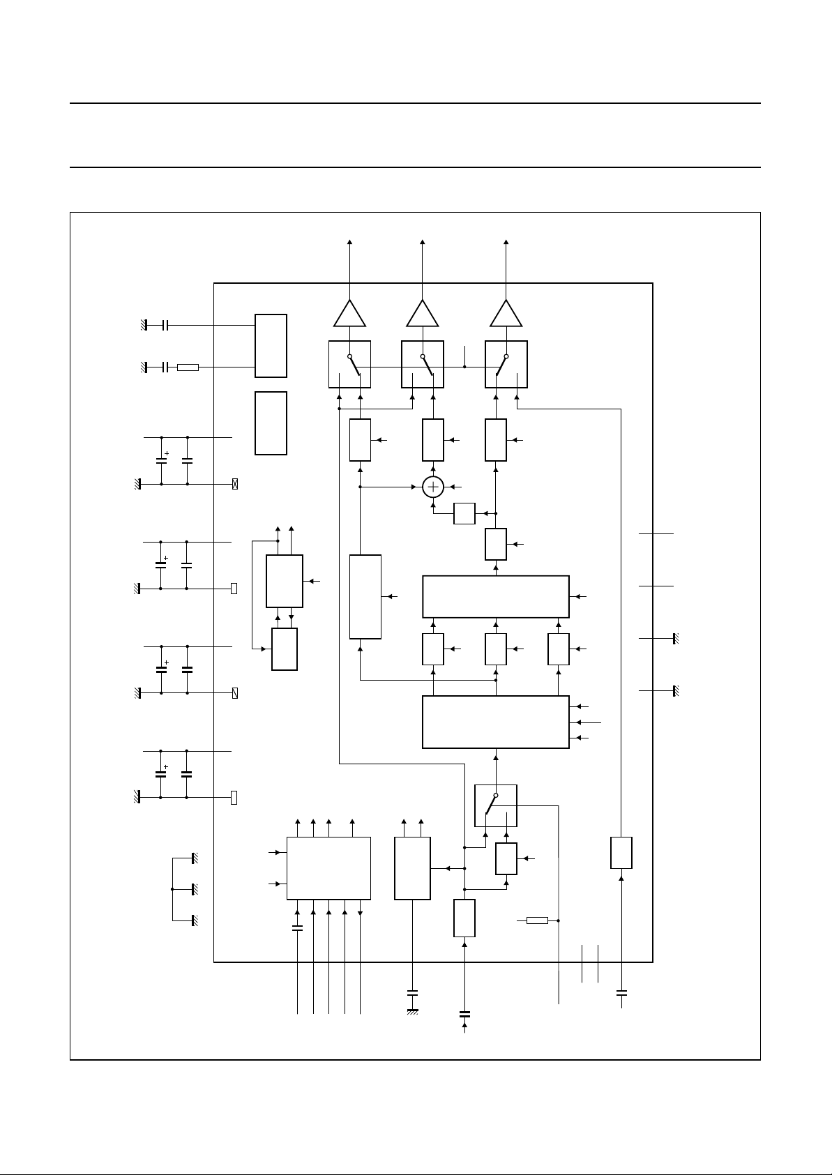
BLOCK DIAGRAM
A
A
+5 V
100 µF
D
+5 V
100 µF
A
handbook, full pagewidth
+5 V
100 µF
A
+5 V
100 nF
100 nF
100 nF
100 nF
100 nF
524
REFBP REFDL
47 Ω
DDD
V
21 22
DGND
CCO
V
OGND
11 8
CCA
V
AGND
97
CCPLL
V
VOLTAGE
REFERENCE
CURRENT
REFERENCE
CONT1
CONT2
LPF
CONTROL
LPFO1
CL3
CVBSO
15
LPFO1
DELAY
S2A
CVBSDL
COMPENSATION
CONT1
CL3
STOPS
CCOMB
CONT1
CL3
−1
CL3
O
C
12
LPFO2
BPF
COMB
FILTER
BPF
S2C
CONT1
CL3
CL3
BPF
SAA4960
CL3
CL3
MHA366
28
4162
i.c. i.c. i.c. i.c.
O
Y
14
S2B
YCOMB
LPFO1
BPF
Fig.1 Block diagram.
CL3
LINES
DELAY
SYSPAL
HSEL
100 nF
100 µF
A
A
D
26 27
PLLGND
DET
V
DET
H
1
FSC
HSEL
3
BYP
CL3
SYSP AL
CLOCK
CONTROL
61325
SSYN
STOPS
FSCSW
COMBENA
H
1996 Oct 15 3
DET
SYNC
19
CSY
A
DET
V
SEPARATOR
100 nF
CLAMP
17
/CVBS
ext
Y
100 nF
S1
LPFI
+5 V
CONT2
18
LPFION
23
n.c.
20
n.c.
BIAS
ext 10
C
100 nF
Remark: all switches in LOW position.
Philips Semiconductors Preliminary specification
Integrated PAL comb filter SAA4960
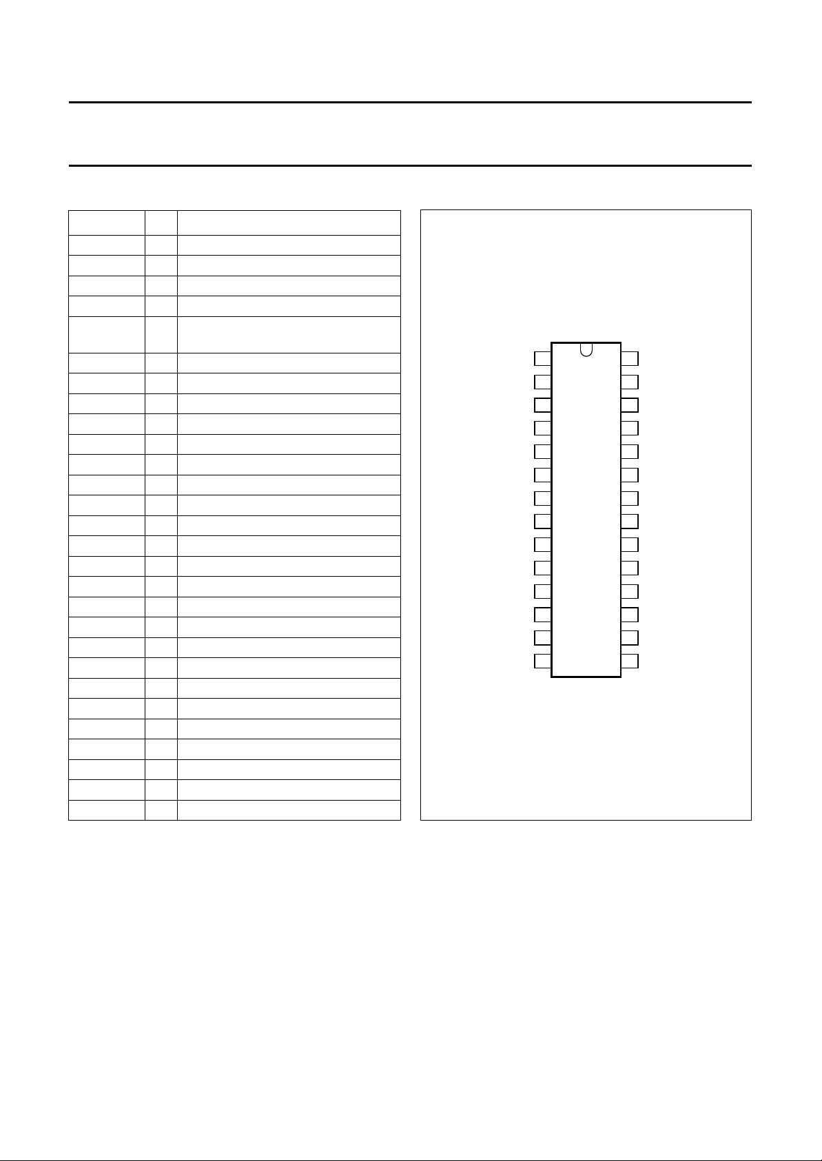
PINNING
SYMBOL PIN DESCRIPTION
FSC 1 subcarrier frequency input
i.c. 2 internally connected
BYP 3 bypass mode forcing input
i.c. 4 internally connected
REFBP
SSYN 6 bypass definition input
V
CCA
V
CCO
AGND 9 analog ground (signal reference)
C
ext
OGND 11 analog ground output buffer
C
O
FSCSW 13 f
Y
O
CVBSO 15 uncombed CVBS output signal
i.c. 16 internally connected
/CVBS 17 CVBS (VBS) input signal
Y
ext
LPFION 18 disable alias-filter
CSY 19 storage capacitor
n.c. 20 not connected
DGND 21 digital ground
V
DDD
n.c. 23 not connected
REFDL 24 decoupling capacitor for delay lines
COMBENA 25 COMB-mode output signal
PLLGND 26 analog ground PLL
V
CCPLL
i.c. 28 internally connected
decoupling capacitor for band-pass
5
filter reference
7 analog supply voltage
8 analog supply voltage output buffer
10 external chrominance input signal
12 chrominance output signal
reference selection input
sc
14 luminance output signal
22 digital supply voltage
27 analog supply voltage PLL
handbook, halfpage
FSC
1
i.c.
2
BYP
3
i.c.
4
REFBP
FSCSW
SSYN
V
CCA
V
CCO
AGND
C
ext
OGND
C
Y
5
6
7
SAA4960
8
9
10
11
12
O
13
O
MHA365
Fig.2 Pin configuration.
28
27
26
25
24
23
22
21
20
19
18
17
16
1514
i.c.
V
CCPLL
PLLGND
COMBENA
REFDL
n.c.
V
DDD
DGND
n.c.
CSY
LPFION
Y
/CVBS
ext
i.c.
CVBSO
1996 Oct 15 4
Philips Semiconductors Preliminary specification
Integrated PAL comb filter SAA4960
FUNCTIONAL DESCRIPTION
Functional requirements
The PAL comb filter processes the video standards PAL B,
G and H. PAL D and I signals can also be processed but
with the drawback of a slightly reduced bandwidth.
For SECAM and SVHS signals, the input signals can be
bypassed to the output without processing by selecting the
BYPASS-mode.
A sync separation circuit is incorporated to generate
control signals for the internal clock processing. With a
sync compression of up to 12 dB the sync separator works
properly (see Fig.4).
The IC is controlled via four pins:
1. BYP forces the IC into the BYPASS-mode (comb filter
function off)
2. SSYN defines whether the COMB-mode is entered
synchronously or not and defines the polarity of the
BYP pin
3. FSCSW selects the reference frequency f
or 2 × f
sc
sc
4. LPFION enables the internal pre-filter.
It is possible to select the following modes of operation:
COMB-mode: Luminance and chrominance comb filter
function active if BYPASS-mode not active.
BYPASS-mode: Signal processing not active, all clocks
inactive, C
Y
/CVBS (pin 17) is bypassed to YO (pin 14) and
ext
(pin 10) is bypassed to CO (pin 12) and
ext
CVBSO (pin 15). This mode is forced via BYP (pin 3).
If the stimulus of the mode is changed, the IC is following
the new mode after the stabilization time given in Table 1.
Table 1 Stabilization time after mode change
MAXIMUM
MODE CHANGE
STABILIZATION
TIME
COMB-mode to BYP ASS-mode 1 line
BYP ASS-mode to COMB-mode 1 field
The mode change from BYPASS to COMB depends on
SSYN (pin 6) and can be asynchronous or synchronous
related to the vertical pulse. The mode change from
COMB to BYPASS is always performed asynchronously.
Pin description
FSC (
PIN 1)
Input for the reference frequency fsc (see note 2 of Chapter
“Characteristics”) or 2 × fsc. For SECAM standard signals
the best signal performance in BYPASS-mode is achieved
by switching the FSC input signal off externally.
BYP (
PIN 3)
Input signal that controls the operation mode. A low-pass
filter is added to the input for suppression of subcarrier
frequencies. Thus applications are supported where the
operation mode (COMB or BYPASS) is controlled by the
DC-level of the FSC input signal at pin 1. For those
applications the BYP input can be externally connected to
FSC (pin 1).
Depending on SSYN (pin 6) the function of BYP can be
adapted to a certain application with respect to the polarity
of the logic level and with respect to the behaviour when
entering the COMB-mode.
Dependent on SSYN the BYP input can be either inverted
or non-inverted with the function as shown in Table 2:
Table 2 Bypass function
SSYN BYP SELECTED MODE
LOW LOW COMB-mode
LOW HIGH BYPASS-mode
HIGH LOW BYPASS-mode
HIGH HIGH COMB-mode
Dependent on SSYN the behaviour when entering the
COMB-mode is different for the both selectable logic
polarities while the BYPASS-mode is always entered
asynchronously (immediately).
Table 3 Behaviour when entering the COMB-mode
SSYN ENTERING COMB-MODE
LOW immediately if BYP = LOW
HIGH synchronized by vertical pulse if BYP = HIGH
The PLL and the clock processing are always stopped if
the selected level for BYPASS is applied to BYP
(independent of the vertical pulse).
1996 Oct 15 5
Philips Semiconductors Preliminary specification
Integrated PAL comb filter SAA4960
REFBP (PIN 5)
Decoupling capacitor for the band-pass filter reference
voltage.
SSYN (
PIN 6)
Input signal that controls the function of BYP (pin 3).
V
CCA,VCCO,VDDD
AND V
(PINS 7, 8, 22 AND 27)
CCPLL
Supply voltages.
AGND, OGND, DGND
AND 26)
21
AND PLLGND (PINS 9, 11,
Ground connection. AGND is used as signal reference for
all analog input and output signals.
(PIN 10)
C
ext
Input for an external chrominance signal which is
correlated to the external VBS signal.
(PIN 12)
C
O
Chrominance output signal. This output can be switched
between the comb filtered chrominance from the CVBS
signal and the external chrominance signal from the input
C
if the IC is forced into BYPASS-mode.
ext
Table 4 C
MODE C
output signal
O
OUTPUT SIGNAL
O
COMB comb filtered chrominance signal
BYPASS external chrominance signal of C
ext
input
Table 6 YO output signal
MODE Y
OUTPUT SIGNAL
O
COMB comb filtered luminance signal
BYPASS external CVBS signal of Y
CVBSO (
PIN 15)
/CVBS input
ext
CVBS output signal directly from the input in
BYPASS-mode or delayed by the signal processing time
of 2 lines and an additional processing delay.
Table 7 CVBSO output signal
MODE CVBSO OUTPUT SIGNAL
COMB delay compensated CVBS signal
BYPASS external CVBS signal of Y
/CVBS (PIN 17)
Y
ext
/CVBS input
ext
Input for the CVBS signal or for an external VBS signal.
LPFION (
PIN 18)
Input signal to disable the internal pre-filter LPFI.
Table 8 Pre-filter mode
LPFION SELECTED MODE
LOW LPFI inactive
HIGH LPFI active
Floating LPFI active
CSY (
PIN 19)
FSCSW (
PIN 13)
Input signal to select between fsc or 2 × fsc as reference at
the FSC input pin.
Table 5 Reference frequency selection
FSCSW SELECTED REFERENCE
HIGH 2 × f
LOW f
(PIN 14)
Y
O
sc
sc
VBS output signal. This output can be switched between
the comb filtered luminance signal (including
synchronization) and the external (C)VBS signal from the
input Y
/CVBS. In COMB-mode the output signal is
ext
delayed by 2 lines and by an additional processing delay.
1996 Oct 15 6
Sync top capacitor for the sync separator.
REFDL (
PIN 24)
Decoupling capacitor for the delay line reference voltage.
COMBENA (
PIN 25)
Output signal that indicates the current mode of operation.
This output is forced to LOW if the comb filter is in
BYPASS-mode.
Table 9 Mode of operation
COMBENA SELECTED MODE
LOW BYP ASS-mode; PLL and clock processing
stopped
HIGH COMB-mode

Philips Semiconductors Preliminary specification
Integrated PAL comb filter SAA4960
Internal functional description
S
WITCHED CAPACITOR DELAY LINE
Delays the CVBS input signal by 2 lines and 4 lines. Input
signals for the delay lines are the CVBS signal, the clock
CL3 (3 × fsc), the control signal HSEL and the standard
selection signal SYSPAL.
Output signals are the non-delayed, the 2-line delayed and
the 4-line delayed CVBS signal.
WITCHED CAPACITOR BAND-PASS FILTERS (BPF)
S
The comb filter input BPFs attenuate the low frequencies
to guarantee a correct signal processing within the logical
comb filter.
The comb filter output BPF reduces the alias components
that are the result of the non-linear signal processing within
the logical comb filter.
OGICAL COMB FILTER
L
Separates the chrominance from the band-pass filtered
CVBS signal.
OMPENSATION DELAY
C
Compensates the internal processing time of the
band-pass filters and the logical comb filter section.
DDER
A
The comb filtered luminance output signal is obtained by
adding the delayed CVBS signal and the inverted comb
filtered chrominance signal.
OW-PASS FILTER INPUT (LPFI)
L
Analog input low-pass filter to reduce the outband
frequencies of EMC. The input low-pass filter is included in
the signal path but it can be switched off via the input
signal LPFION.
OW-PASS FILTER OUTPUT (LPFO1 AND LPFO2)
L
Two different types of output low-pass filters (LPFO1 and
LPFO2) are necessary to get equal signal delays within the
luminance path and the chrominance path (important for
good transient behaviour). The low-pass output filter type
LPFO1 is used for the luminance output while LPFO2 is
used for the chrominance output. The filters are analog 3
order elliptic low-pass filters that convert the output signals
from the time discrete to the time continuous domain
(reconstruction filter).
LPF
CONTROL
Automatic tuning of the low-pass filters is achieved by
adjusting the filter delays. The control information for all
filters (CONT1 and CONT2) is derived from a built-in
reference filter (LPFO1-type) that is part of a control loop.
The control loop tunes the reference filter delay and thus
all other filter delays to a time constant derived from the
system clock CL3.
C
ONTROL AND CLOCK PROCESSING (CLOCK CONTROL)
The control and clock processing block (see Fig.7)
consists of the sub-blocks PLL, the clock processing and
the mode control. The PLL and the clock processing are
released for operation if the input level at BYP selects the
COMB-mode.
Main tasks of the control and clock processing are:
• Clock generation of system clock CL3
• Delay line start control
• Mode control.
The signal processing is based on a 3 × fsc system clock
(CL3), that is generated by the clock processing from the
fscsignal at FSC (pin 1) via a PLL. Because the subcarrier
frequency divided by the line frequency results not in an
integer value a clock phase correction of 180° is necessary
every second line for PAL standards. The clock phase
correction is controlled by the input signals horizontal
sync. Additionally the delay line start is synchronized once
a field to the input signals horizontal sync. The 25 Hz PAL
offset is corrected in this way.
The PLL provides a master clock MCK of 6 × fsc, which is
locked to the subcarrier frequency at FSC (pin 1).
The system clock CL3 (3 × fsc) is obtained from MCK by a
divide-by-two circuit. The 180° phase shift is generated by
stopping the divide-by-two circuit for one MCK clock cycle.
The generated clock is a pseudo-line-locked clock that is
referenced to fsc. The sync separator generates the
necessary signals H
DET
and V
indicating the line (H)
DET
and the field (V) sync periods.
The current mode of operation (BYPASS or COMB) is
external readable via COMBENA (pin 25).
rd
1996 Oct 15 7
Philips Semiconductors Preliminary specification
Integrated PAL comb filter SAA4960
The input signals of the control and clock processing
(CLOCK CONTROL) are:
H
: analog horizontal pulse from sync separator
DET
V
: analog vertical pulse from sync separator
DET
FSC: subcarrier frequency (fsc or 2 × fsc)
FSCSW: reference frequency selection
BYP: BYPASS control signal
SSYN: vertical synchronous mode selection for BYP
and polarity selection of BYP.
The output signals are:
CL3: system clock (3 × fsc)
HSEL’s: line start signals for the delay lines
STOPS: forces the comb filter via the switches S2A,
S2B and S2C into the BYPASS-mode (always
asynchronous) or COMB-mode (synchronous or
asynchronous with V
; depending on SSYN)
INT
COMBENA: HIGH during COMB-mode; otherwise
LOW.
Table 10 Function of STOPS signal
STOPS-STATE SELECTED MODE
LOW COMB
HIGH BYPASS
Table 11 Function of signal switch S1
LPFION-STATE DELAY LINE INPUT
LOW non-pre-filtered input signal
/CVBS
Y
ext
HIGH pre-filtered input signal Y
Floating pre-filtered input signal Y
IGNAL SWITCH S2A
S
/CVBS
ext
/CVBS
ext
For the CVBSO output two signals can be selected via the
signal switch S2A.
Table 12 CVBSO output signal
STOPS-STATE
CVBSO OUTPUT
SIGNAL
MODE
LOW delayed input CVBSDL COMB
HIGH non-delayed input
/CVBS
Y
ext
BYPASS
SIGNAL SWITCHES S2B AND S2C
Two switches are included to bypass the comb filter signal
processing. The input video signal C
for the switch S2C
ext
is internally biased.
For the YO output two signals can be selected via S2B.
H
ORIZONTAL AND VERTICAL SYNC SEPARATOR
A build-in sync separator circuit generates the H
V
signals from the Y
DET
/CVBS input signal. This circuit
ext
DET
and
is still working properly at input signals with a 12 dB
attenuated sync in a normal 700 mV black-to-white video
signal (see Fig.4).
LAMP
C
The black level clamping of the video input signal is
performed by the sync separator stage. The clamping level
is nearly adequate to the voltage at REFDL (pin 24).
IGNAL SWITCH S1
S
The switch is included to bypass the low-pass input filter.
For the CVBS input of the delay line block two signals can
be selected via the slow signal switch S1.
Table 13 Y
STOPS-STATE Y
output signal
O
OUTPUT SIGNAL MODE
O
LOW YCOMB
(combed luminance)
HIGH input Y
For the C
Table 14 C
STOPS-STATE C
output two signals can be selected via S2C.
O
output signal
O
OUTPUT SIGNAL MODE
O
LOW CCOMB
(combed chrominance)
HIGH input C
COMB
/CVBS BYPASS
ext
COMB
ext
BYPASS
1996 Oct 15 8
 Loading...