

Philips SAA4956TJ-V1 Datasheet
DATA SH EET
Preliminary specification
File under Integrated Circuits, IC02
1998 Dec 08
INTEGRATED CIRCUITS
SAA4956TJ
2.9-Mbit field memory with noise
reduction

1998 Dec 08 2
Philips Semiconductors Preliminary specification
2.9-Mbit field memory with noise reduction SAA4956TJ
CONTENTS
1 FEATURES
2 GENERAL DESCRIPTION
3 ORDERING INFORMATION
4 QUICK REFERENCE DATA
5 BLOCK DIAGRAM
6 PINNING
7 FUNCTIONAL DESCRIPTION
7.1 Field memory function
7.1.1 Write operation
7.1.2 Read operation
7.1.3 Power-up and initialization
7.1.4 Old and new data access
7.1.5 Memory arbitration logic and self-refresh
7.1.6 Cascade operation
7.1.7 Test mode operation
7.2 Noise reduction function
7.2.1 Reformatting and formatting
7.2.2 Band-splitting
7.2.3 Motion detection
7.2.4 K-factor
7.2.5 Noise shape
7.3 I2C-bus interface
8 LIMITING VALUES
9 THERMAL CHARACTERISTICS
10 CHARACTERISTICS
11 APPLICATION INFORMATION
12 PACKAGE OUTLINE
13 SOLDERING
13.1 Introduction to soldering surface mount
packages
13.2 Reflow soldering
13.3 Wave soldering
13.4 Manual soldering
13.5 Suitability of surface mount IC packages for
wave and reflow soldering methods
14 DEFINITIONS
15 LIFE SUPPORT APPLICATIONS
16 PURCHASE OF PHILIPS I2C COMPONENTS

1998 Dec 08 3
Philips Semiconductors Preliminary specification
2.9-Mbit field memory with noise reduction SAA4956TJ
1 FEATURES
• 2949264-bit field memory with optional field based
noise reduction
• 245772 × 12-bit organization
• 3.3 V power supply
• Inputs fully TTL compatible when using an extra 5 V
power supply
• High speed read and write operations
• FIFO operations:
– Full word continuous read and write
– Independent read and write pointers (asynchronous
read and write access)
– Resettable read and write pointers.
• Optional field based noise reduction activated by an
enable pin and controlled via the I
2
C-bus
• Optional random access by block function (40 words per
block) enabled during pointer reset operation
• Quasi static (internal self-refresh and clocking pauses of
infinite length)
• Write mask function
• Cascade operation possible
• Compatible with SAA4955TJ
• 16-Mbit CMOS DRAM process technology
• 40-pin SOJ package.
2 GENERAL DESCRIPTION
The SAA4956TJ is a 2949264-bit field memory with an
optional field based noise reduction designed for
advanced TV applications such as 100/120 Hz TV,
PALplus, PIP and 3D comb filter. The SAA4956TJ is
functional and pin compatible with the SAA4955TJ.
However, the SAA4956TJ has also, in addition to the field
memory function, a field based noise reduction circuit. If
this function is enabled it can be controlled via the I
2
C-bus.
The maximum storage depth is 245772 words × 12 bits.
A FIFO operation with full word continuous read and write
could be used as a data delay, for example. A FIFO
operation with asynchronous read and write could be used
as a data rate multiplier. Here the data is written once, then
read as many times as required as long as new data is not
written. In addition to the FIFO operations, a random block
access mode is accessible during the pointer reset
operation. When this mode is enabled, reading and/or
writing may begin at, or proceed from, the start address of
any of the 6144 blocks. Each block is 40 words in length.
Two or more SAA4956TJs can be cascaded to provide a
greater storage depth or a longer delay, without the need
for additional circuitry.
The SAA4956TJ contains separate 12-bit wide serial ports
for reading and writing. The ports are controlled and
clocked separately, so asynchronous read and write
operations are supported. Independent read and write
clock rates are possible. Addressing is controlled by read
and write address pointers. Before a controlled write
operation can begin, the write pointer must be set to zero
or to the beginning of a valid address block. Likewise, the
read pointer must be set to zero or to the beginning of a
valid address block before a controlled read operation can
begin.
3 ORDERING INFORMATION
TYPE
NUMBER
PACKAGE
NAME DESCRIPTION VERSION
SAA4956TJ SOJ40 plastic small outline package; 40 leads (J-bent); body width 10.16 mm SOT449-1
1998 Dec 08 4
Philips Semiconductors Preliminary specification
2.9-Mbit field memory with noise reduction SAA4956TJ
4 QUICK REFERENCE DATA
SYMBOL PARAMETER CONDITIONS MIN. TYP. MAX. UNIT
T
cy(SWCK)
SWCK cycle time NREN = LOW; see Fig.4 26 − − ns
NREN = HIGH; see Fig.4
52 − 150 ns
T
cy(SRCK)
read cycle time (SRCK) see Fig.11 26 − − ns
t
ACC
read access time after SRCK see Fig.11 −−21 ns
V
DD
supply voltage (pin 19) 3.0 3.3 3.6 V
V
DD(O)
supply voltage (pin 22) 3.0 3.3 3.6 V
V
DD(P)
supply voltage (pin 21) 3.0 3.3 5.5 V
I
DD(tot)
total supply current
(I
DD(tot)=IDD+IDD(O)+IDD(P)
)
minimum read/write cycle;
outputs open
− 27 70 mA
1998 Dec 08 5
Philips Semiconductors Preliminary specification
2.9-Mbit field memory with noise reduction SAA4956TJ
5 BLOCK DIAGRAM
Fig.1 Block diagram.
Pin 21 (V
DD(P)
) should be connected to the supply voltage of the driving circuit that generates the input voltages. This could be, for instance, 5.0 V
instead of 3.3 V. Pins19 and 22 (V
DD
and V
DD(O)
) require a 3.3 V supply.
handbook, full pagewidth
MGR687
SERIAL WRITE REGISTER
20-WORD (×13)
mini cache write/read2 control + cache transfer
mini cache read control
OE
internal
DATA MUX
D-field delay
PARALLEL WRITE REGISTER
20-WORD (×13)
20 × (12 + 1)
I2C-bus control
12 + 1
12
12
12
MEMORY ARRAY
245760-WORD (×12)
SAA4956TJ
MEMORY
ARBITRATION
LOGIC
WRITE ADDRESS
COUNTER
REFRESH ADDRESS
COUNTER
READ ADDRESS
COUNTER
WRITE REGISTER
DATA INPUT AND
WRITE MASK
BUFFER (×13)
INPUT BUFFER
(×3)
SERIAL WRITE/READ2 CONTROLLER
CLOCK
OSCILLATOR
IE
internal
OE
internal
D0
internal
20 × (12 + 1)
12
27 to 38 23
OE
Q0
(V0)
to Q11
(Y7)
D0
(V0)
to D11
(Y7)
RE RSTR SRCK
24 25 26
12
22
100 nF
12
14 to 3 18
17 16 15
12 + 1
12 + 1
+3.3 V
READ
REGISTER
READ2
REGISTER
MINI CACHE
12-WORD (×12)
DATA MUX
DATA OUTPUT
BUFFER (×12)
INPUT BUFFER
(×4)
DATA
MUX
NOISE
REDUCTION
12
READ2 ADDRESS
COUNTER
IE internal
D0 internal
SERIAL READ CONTROLLER
3
3
write
control
read2
control
write
acknowledge
read2
acknowledge
read
control
PARALLEL READ REGISTER
20-WORD (×12)
20 × 12
SERIAL READ REGISTER
20-WORD (×12)
20 × 12
PARALLEL READ2 REGISTER
20-WORD (×12)
20 × 12
SERIAL READ2 REGISTER
20-WORD (×12)
20 × 12
read
acknowledge
load write
block
address
load read
block
address
refresh
clock
IE
internal
IE WE RSTW SWCK
40 1 20
NREN SCL SDA
2
GND
39
OGND
V
DD(O)
21
V
DD(P)
19
V
DD
I2C-BUS
INTERFACE
1998 Dec 08 6
Philips Semiconductors Preliminary specification
2.9-Mbit field memory with noise reduction SAA4956TJ
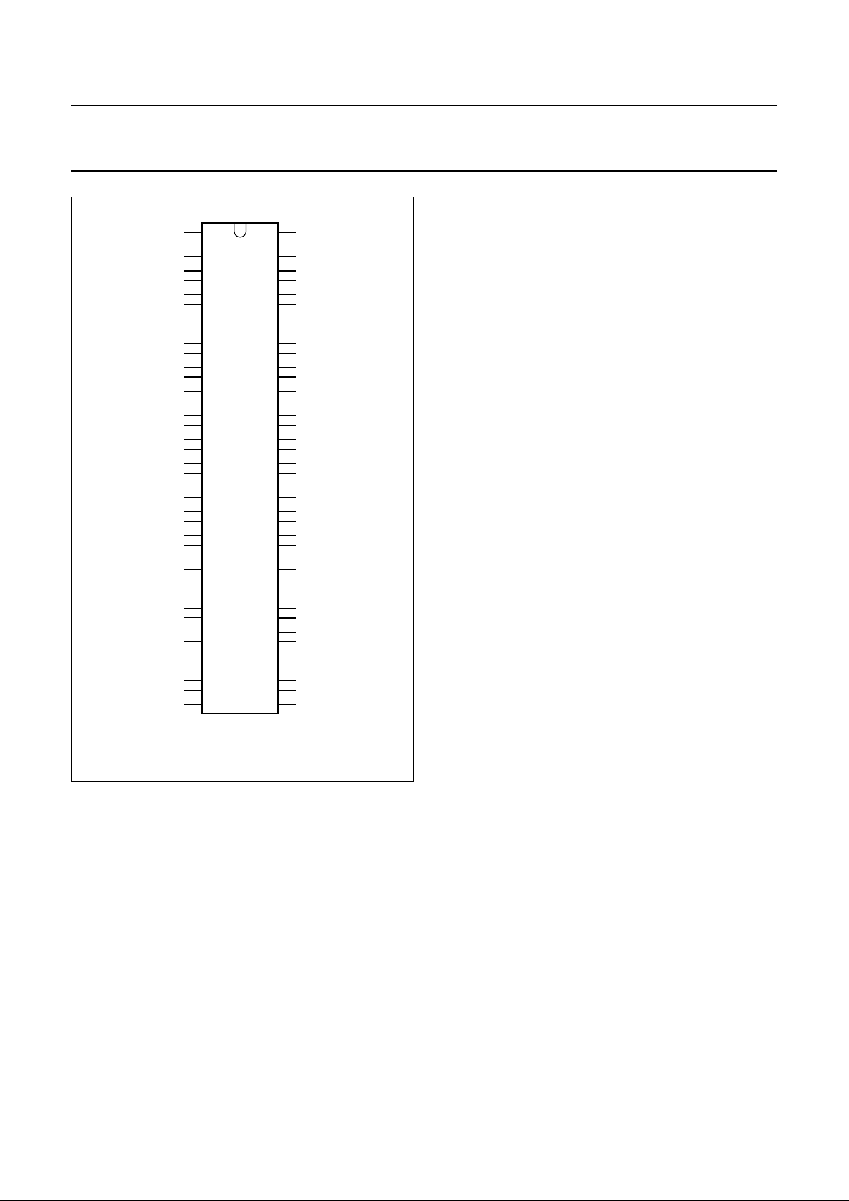
6 PINNING
SYMBOL PIN I/O DESCRIPTION
SCL 1 digital input serial clock of I
2
C-bus
GND 2 ground general purpose ground
D11
(Y7)
3 digital input data input 11, Y input bit 7 if NREN is HIGH
D10
(Y6)
4 digital input data input 10, Y input bit 6 if NREN is HIGH
D9
(Y5)
5 digital input data input 9, Y input bit 5 if NREN is HIGH
D8
(Y4)
6 digital input data input 8, Y input bit 4 if NREN is HIGH
D7
(Y3)
7 digital input data input 7, Y input bit 3 if NREN is HIGH
D6
(Y2)
8 digital input data input 6, Y input bit 2 if NREN is HIGH
D5
(Y1)
9 digital input data input 5, Y input bit 1 if NREN is HIGH
D4
(Y0)
10 digital input data input 4, Y input bit 0 if NREN is HIGH
D3
(U1)
11 digital input data input 3, U input bits 1, 3, 5, 7 if NREN is HIGH
D2
(U0)
12 digital input data input 2, U input bits 0, 2, 4, 6 if NREN is HIGH
D1
(V1)
13 digital input data input 1, V input bits 1, 3, 5, 7 if NREN is HIGH
D0
(V0)
14 digital input data input 0, V input bits 0, 2, 4, 6 if NREN is HIGH
SWCK 15 digital input serial write clock
RSTW 16 digital input write reset clock
WE 17 digital input write enable
IE 18 digital input input enable
V
DD
19 supply 3.3 V general purpose supply voltage
SDA 20 digital I/O serial data of I
2
C-bus
V
DD(P)
21 supply 3.3 to 5.5 V supply voltage for protection circuits
V
DD(O)
22 supply 3.3 V supply voltage for output circuits
OE 23 digital input output enable
RE 24 digital input read enable
RSTR 25 digital input reset read
SRCK 26 digital input serial read clock
Q0
(V0)
27 digital output data output 0, V output bits 0, 2, 4, 6 if NREN is HIGH
Q1
(V1)
28 digital output data output 1, V output bits 1, 3, 5, 7 if NREN is HIGH
Q2
(U0)
29 digital output data output 2, U output bits 0, 2, 4, 6 if NREN is HIGH
Q3
(U1)
30 digital output data output 3, U output bits 1, 3, 5, 7 if NREN is HIGH
Q4
(Y0)
31 digital output data output 4, Y output bit 0 if NREN is HIGH
Q5
(Y1)
32 digital output data output 5, Y output bit 1 if NREN is HIGH
Q6
(Y2)
33 digital output data output 6, Y output bit 2 if NREN is HIGH
Q7
(Y3)
34 digital output data output 7, Y output bit 3 if NREN is HIGH
Q8
(Y4)
35 digital output data output 8, Y output bit 4 if NREN is HIGH
Q9
(Y5)
36 digital output data output 9, Y output bit 5 if NREN is HIGH
Q10
(Y6)
37 digital output data output 10, Y output bit 6 if NREN is HIGH
Q11
(Y7)
38 digital output data output 11, Y output bit 7 if NREN is HIGH
OGND 39 ground ground for output circuits
NREN 40 digital input noise reduction enable
1998 Dec 08 7
Philips Semiconductors Preliminary specification
2.9-Mbit field memory with noise reduction SAA4956TJ
7 FUNCTIONAL DESCRIPTION
The functional description is divided into 3 main sections:
• The basic field memory function (see Section 7.1)
• The optional noise reduction function (used in case the
NREN signal is HIGH; see Section 7.2)
• The I2C-bus interface function (which controls the noise
reduction circuit; see Section 7.3).
7.1 Field memory function
The basic field memory function is fully compatible with the
SAA4955TJ if the NREN signal is LOW. In this case the
noise reduction function is bypassed via a data mux. If the
NREN signal is HIGH the basic field memory function can
only be executed with a write frequency restricted to half of
Fig.2 Pin configuration.
handbook, halfpage
SAA4956TJ
MGR688
1
2
3
4
5
6
7
8
9
10
11
12
13
14
15
16
17
18
19
20
40
39
38
37
36
35
34
33
32
31
30
29
28
27
26
25
24
23
22
21
NREN
OGND
Q0
(V0)
Q1
(V1)
Q2
(U0)
Q3
(U1)
Q4
(Y0)
Q5
(Y1)
Q6
(Y2)
Q7
(Y3)
Q8
(Y4)
Q9
(Y5)
Q10
(Y6)
Q11
(Y7)
SRCK
RSTR
RE
OE
V
DD(O)
V
DD(P)
SCL
GND
D11
(Y7)
D10
(Y6)
D9
(Y5)
D8
(Y4)
D7
(Y3)
D6
(Y2)
D5
(Y1)
D4
(Y0)
D3
(U1)
D2
(U0)
D1
(V1)
D0
(V0)
SWCK
RSTW
WE
IE
V
DD
SDA
the read operation frequency. In this case the random
block access modes are not supported because a second
read operation (READ2) is activated with an identical
frequency as used in the write operations. The PAN-IC
(SAA4995WP) needs approximately the same write
frequency for the noise reduction option as the read
frequency (32 MHz). To allow this configuration the
self-refresh must be switched off via the I2C-bus interface.
7.1.1 W
RITE OPERATION
Write operations are controlled by the SWCK, RSTW, WE
and IE signals. A write operation starts with a reset write
address pointer (RSTW) operation, followed by a complete
cycle of the SWCK clock during which time WE and IE
must be held HIGH. Write operations between two
successive reset write operations must contain at least
40 SWCK write clock cycles while WE is HIGH. To transfer
data temporarily stored in the serial write registers to the
memory array, a reset write operation is required after the
last write operation.
7.1.1.1 Reset write: RSTW
The first positive transition of SWCK after RSTW goes
from LOW-to-HIGH resets the write address pointer to the
lowest address (−12 decimal), regardless of the state of
WE (see Figs 4 and 5). RSTW set-up (t
su(RSTW)
) and hold
(t
h(RSTW)
) times are referenced to the rising edge of SWCK
(see Fig.4). The reset write operation may also be
asynchronously related to the SWCK signal if WE is LOW.
RSTW needs to stay LOW for a single SWCK cycle before
another reset write operation can take place. If RSTW is
HIGH for 1024 SWCK write clock cycles while WE is
HIGH, the SAA4956TJ will enter a built-in test mode.
7.1.1.2 Random write block access mode
The SAA4956TJ will enter random write block access
mode if the following signal sequence is applied to control
inputs IE and WE during the first four SWCK write clock
cycles after a reset write (see Figs 6 and 7):
1. At the 1st and 2nd positive transitions of SWCK,
IE must be LOW and WE must be HIGH
2. At the 3rd and 4th positive transitions of SWCK,
IE must be HIGH and WE must be LOW
3. At the 5th positive transition of SWCK, the state of WE
determines which input pin is used for the block
address. If WE is LOW the Most Significant Bit (MSB)
of the block address must be applied to the D0 input
pin. If WE is HIGH, the MSB of the block address is
applied to pin IE.

1998 Dec 08 8
Philips Semiconductors Preliminary specification
2.9-Mbit field memory with noise reduction SAA4956TJ
During this time, control signals WE and IE will function as
defined for normal operation. The remaining 12 bits of the
13-bit write block address must be applied, in turn, to the
selected input pin (D0 or IE) at the following 12 positive
transitions of SWCK. The Least Significant Bit (LSB) of the
write block address is applied at the 17th positive
transition of SWCK. A write latency period of 18 additional
SWCK clock cycles is required before write access to the
new block address is possible. During this time, data is
transferred from the serial write and parallel write registers
into the memory array and the write pointer is set to the
new block address.
Block address values between 0 and 6143 are valid.
Values outside this range must be avoided because invalid
block addresses can result in abnormal operation or a
lock-up condition. Recovery from lock-up requires a
standard reset write operation.
WE must remain LOW from the 3rd positive transition of
SWCK to the 17th write latency SWCK clock cycle if the
block address is applied to pin D0. If the block address is
applied to pin IE, WE must be HIGH on the 5th positive
transition of SWCK, may be HIGH or LOW on the
6th transition, and must be LOW from the 7th transition to
the 17th write latency SWCK clock cycle.
At the 18th write latency SWCK clock cycle, IE and WE
may be switched HIGH to prepare for writing new data at
the next positive transition of SWCK. The complete write
block access entry sequence is finished after the
18th write latency cycle.
The LOW-to-HIGH transition on RSTW required at the
beginning of the sequence should not be repeated.
Additional LOW-to-HIGH transitions on RSTW would
disable write block address mode and reset the write
pointer.
7.1.1.3 Address organization
Two different types of memory are used in the data
address area: a mini cache for the first 12 data words after
a reset write or a reset read, and a DRAM cell memory
array with a 245760 word capacity. Each word is 12 bits
long. The mini cache is needed to store data temporarily
after a reset operation since a latency period is required
before read or write access to the memory array is
possible. Latency periods are needed for read or write
operations in random read or write block access modes
because data is read from, or written to, the memory array.
The data in the mini cache can only be accessed directly
after a standard reset operation. It cannot be accessed in
random read or write block access modes.
The address area reserved for the mini cache, accessible
after a standard reset operation, is from decimal−12 to −1.
The memory array starts at decimal 0 and ends at 245759.
Decimal address 0 is identical to block address 0000H.
Because a single block address is defined for every
40 words in the memory array, block address 0001H
corresponds to decimal address 40. The highest block
address is 17FFH. This block has a decimal start address
of 245720 and an end address of 245759.
If a read or write reset operation is not performed, the next
read or write pointer address after 245759 will be
address 0 due to pointer wraparound. It should be noted
that reset read and write operations should occur together.
If one pointer wraps around while the other is reset, either
12 words will be lost or 12 words of undefined data will be
read.
7.1.1.4 Data inputs: D0 to D11 and write clock: SWCK
A positive transition on the SWCK write clock latches the
data on inputs D0 to D11, provided WE was HIGH at the
previous positive transition of SWCK. The data input
set-up (t
su(D)
) and hold (t
h(D)
) times are referenced to the
positive transition of SWCK (see Fig.5). The latched data
will only be written into memory if IE was HIGH at the
previous positive transition of SWCK.
7.1.1.5 Write enable: WE
Pin WE is used to enable or disable a data write operation.
The WE signal controls data inputs D0 to D11. In addition,
the internal write address pointer is incremented if WE is
HIGH at the positive transition of the SWCK write clock.
WE set-up (t
su(WE)
) and hold (t
h(WE)
) times are referenced
to the positive edge of SWCK (see Fig.8).
7.1.1.6 Input enable: IE
Pin IE is used to enable or disable a data write operation
from the D0 to D11 data inputs into memory. The latched
data will only be written into memory if the IE and WE
signals were HIGH during the previous positive transition
of SWCK. A LOW level on IE will prevent the data being
written into memory and existing data will not be
overwritten (write mask function; see Fig.10). The IE
set-up (t
su(IE)
) and hold (t
h(IE)
) times are referenced to the
positive edge of SWCK (see Fig.9).

1998 Dec 08 9
Philips Semiconductors Preliminary specification
2.9-Mbit field memory with noise reduction SAA4956TJ
7.1.2 READ OPERATION
Read operations are controlled by the SRCK, RSTR, RE
and OE signals. A read operation starts with a reset read
address pointer (RSTR) operation, followed by a complete
cycle of the SRCK clock during which time RE and OE
must be held HIGH. Read operations between two
successive reset read operations must contain at least
20 SRCK read clock cycles while RE is HIGH.
7.1.2.1 Reset read: RSTR
The first positive transition of SRCK after RSTR goes from
LOW-to-HIGH resets the read address pointer to the
lowest address (−12 decimal; see Figs 11 and 12). If RE is
LOW, however, the reset read operation to the lowest
address will be delayed until the first positive transition of
SRCK after RE goes HIGH. RSTR set-up (t
su(RSTR)
) and
hold (t
h(RSTR)
) times are referenced to the rising edge of
SRCK (see Fig.11). The reset read operation may also be
asynchronously related to the SRCK signal if RE is LOW.
RSTR needs to stay LOW for a single SRCK cycle before
another reset write operation can take place.
7.1.2.2 Random read block access mode
The SAA4956TJ will enter random read block access
mode if the following signal sequence is applied to control
inputs RE and OE during the first four SWCK write clock
cycles after a reset read (see Fig.13):
1. At the 1st and 2nd positive transitions of SRCK,
OE must be LOW and RE must be HIGH
2. At the 3rd and 4th positive transitions of SRCK,
OE must be HIGH and RE must be LOW.
During this time, control signals RE and OE will function as
defined for normal operation. The Most Significant Bit
(MSB) of the block read address is applied to the OE input
pin at the 5th positive transition of SRCK. The remaining
12 bits of the 13-bit read block address must be applied, in
turn, to OE at the following 12 positive transitions of
SWCK. The Least Significant Bit (LSB) of the block
address is applied at the 17th positive transition of SRCK.
A read latency period of 20 additional SRCK clock cycles
is required before read access to the new block address is
possible. During this period, data is transferred from the
memory array to the serial read and parallel read registers
and the read pointer is set to the new block address.
Block address values between 0 and 6143 are valid.
Values outside this range must be avoided because invalid
block addresses can result in abnormal operation or a
lock-up condition. Recovery from lock-up requires a
standard reset read operation.
The data output pins are not controlled by the OE pin and
are forced into high impedance mode from the 3rd to
the 17th positive transition of SRCK. OE should be held
LOW during the read latency period. RE must remain LOW
from the 3rd positive transition of SRCK to the 20th read
latency SRCK clock cycle.
After the 20th read latency SRCK clock cycle, RE and OE
may be switched HIGH to prepare for reading new data
from the new address block at the next positive transition
of SRCK. The complete read block access entry sequence
is finished after the 20th read latency cycle.
The LOW-to-HIGH transition on RSTR required at the
beginning of the sequence should not be repeated.
Additional LOW-to-HIGH transitions on RSTR would
disable the read block address mode and reset the read
pointer.
7.1.2.3 Data outputs: Q0 to Q11 and read clock:
SRCK
The new data is shifted out of the data output registers on
the rising edge of the SRCK read clock provided RE and
OE are HIGH. Data output pins are low impedance if OE is
HIGH. If OE is LOW, the data outputs are high impedance
and the data output bus may be used by other devices.
Data output hold (t
h(Q)
) and access times (t
ACC
) are
referenced to the positive transition of SRCK. The output
data becomes valid after access time interval t
ACC
(see
Fig.12).
Data output pins Q0 to Q11 are TTL compatible with the
restriction that when the outputs are high impedance, they
must not be forced higher than V
DD(O)
+ 0.5 V or 5.0 V
absolute. The output data has the same polarity as the
incoming data at inputs D0 to D11.
7.1.2.4 Read enable: RE
RE is used to increment the read pointer. Therefore, RE
needs to be HIGH at the positive transition of SRCK. When
RE is LOW, the read pointer is not incremented. RE set-up
(t
su(RE)
) and hold times (t
h(RE)
) are referenced to the
positive edge of SRCK (see Fig.14).
7.1.2.5 Output enable: OE
OE is used to enable or disable data outputs Q0 to Q11.
The data outputs are enabled (low impedance) if OE is
HIGH. OE LOW disables the data output pins (high
impedance). Incrementing of the read pointer does not
depend on the status of OE. OE set-up (t
su(OE)
) and hold
times (t
h(OE)
) are referenced to the positive edge of SRCK
(see Fig.15).

1998 Dec 08 10
Philips Semiconductors Preliminary specification
2.9-Mbit field memory with noise reduction SAA4956TJ
7.1.3 POWER-UP AND INITIALIZATION
Reliable operation is not guaranteed until at least 100 µs
after power-up, the time needed to stabilize VDD within the
recommended operating range. After the 100 µs power-up
interval has elapsed, the following initialization sequence
must be performed: a minimum of 12 dummy read
operations (SRCK cycles) followed by a reset read
operation (RSTR), and a minimum of 12 dummy write
operations (SWCK) followed by a reset write operation
(RSTW). Read and write initialization may be performed
simultaneously.
If initialization starts earlier than the recommended 100 µs
after power-up, the initialization sequence described
above must be repeated, starting with an additional reset
read operation and an additional reset write operation after
the 100 µs start-up time.
7.1.4 O
LD AND NEW DATA ACCESS
A minimum delay of 40 SWCK clock cycles is needed
before newly written data can be read back from memory
(see Fig.16). If a reset read operation (RSTR) occurs in a
read cycle before a reset write operation (RSTW) in a write
cycle accessing the same location, then old data will be
read.
Old data will be read provided a data read cycle begins
within 20 pointer positions of the start of a write cycle. This
means that if a reset read operation begins within
20 SWCK clock cycles after a reset write operation, the
internal buffering of the SAA4956TJ will ensure that old
data will be read out (see Fig.17).
New data will be read if the read pointer is delayed by
40 pointer positions or more after the write pointer.
Old data is still read out if the write pointer is less than or
equal to 20 pointer positions ahead of the read pointer
(internal buffering). A write pointer to read pointer delay of
more than 20 but less than 40 pointer positions should be
avoided. In this case, the old or the new data may be read,
or a combination of both.
In random read and write block access modes, the
minimum write-to-read new data delay of 40 SWCK clock
cycles must be inserted for each block.
7.1.5 M
EMORY ARBITRATION LOGIC AND SELF-REFRESH
Since the data in the memory array is stored in DRAM
cells, it needs to be refreshed periodically. Refresh is
performed automatically under the control of internal
memory arbitration logic which is clocked by a free running
clock oscillator. The memory arbitration logic controls
memory access for read, write and refresh operations.
It uses the contents of the write, read and refresh address
counters to access the memory array to load data from the
parallel write register, store data in the parallel read
register, or to refresh stored data. The values in these
counters correspond to block addresses.
7.1.6 C
ASCADE OPERATION
If a longer delay is needed, the total storage depth can be
increased beyond 2949264 bits by cascading several
SAA4956TJs. For details see the interconnection and
timing diagrams (Figs 18 and 19).
The noise reduction function can be realized by enabling
this function with the NREN pin at one of the cascaded
SAA4956TJs.
7.1.7 T
EST MODE OPERATION
The SAA4956TJ incorporates a test mode not intended for
customer use. If WE and RSTW are held HIGH
continuously for 1024 SWCK clock cycles, the
SAA4956TJ will enter test mode. It will exit test mode if WE
is LOW for a single SWCK cycle or if RSTW is LOW for
2 SWCK clock cycles.
1998 Dec 08 11
Philips Semiconductors Preliminary specification
2.9-Mbit field memory with noise reduction SAA4956TJ
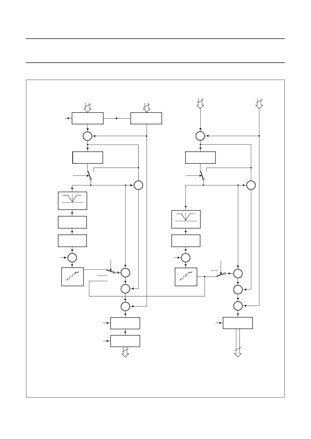
7.2 Noise reduction function
Fig.3 Block diagram of noise reduction.
Switch position is off.
handbook, full pagewidth
8
×
+
+
+
data input
D11
(Y7)
to D4
(Y0)
8
D-field delay
D11
(Y7)
to D4
(Y0)
8
D to memory
D11
(Y7)
to D4
(Y0)
new Y old Y
delta Y
LF delta Y
−
−
LOW-PASS
FILTER 1
LOW-PASS
FILTER 2
NOISE SHAPE
ABS/LIMITER
LUT
I2C-bus control:
Yadapt_gain
I2C-bus control:
noise_shape
I2C-bus control:
lumafix
+
Kluma
Klumafix
processed Y
4
×
×
×
+
+
+
data input
4
D-field delay
new U/V old U/V
delta U/V
LF delta U/V
HF
delta
U/V
HF
delta
Y
−
−
LOW-PASS
FILTER 1
LOW-PASS
FILTER 2
U/V
AVERAGE
NOISE SHAPE
ABS/LIMITER
LUT
I2C-bus control:
unfiltered
I
2
C-bus control:
chroma_inverted
DPCMin
I
2
C-bus control:
Cadapt_gain
I2C-bus control:
noise_shape
I2C-bus control:
chromafix and
Klumatochroma
REFORMATTER REFORMATTER
+
4
D to memory
D0
(V0)
, D1
(V1)
D2
(U0)
, D3
(U1)
D0
(V0)
, D1
(V1)
D2
(U0)
, D3
(U1)
D0
(V0)
, D1
(V1)
D2
(U0)
, D3
(U1)
FORMATTER
I2C-bus control:
DPCMout
MGR689
Kchromafix
Kluma
Kchroma
processed U/V
I2C-bus control:
unfiltered
 Loading...