

Philips saa4952wp DATASHEETS

INTEGRATED CIRCUITS
DATA SH EET
SAA4952WP
Memory controller
Objective specification
File under Integrated Circuits, IC02
1997 Jun 10
Philips Semiconductors Objective specification
Memory controller SAA4952WP
FEATURES
• Support for acquisition, display and deflection PLL
• 50/100 Hz (or 60/120 Hz) scan conversion
• Progressive scan 50 Hz/1250 lines (60 Hz/1050 lines)
interlaced or 50 Hz/625 lines (60 Hz/525 lines)
non-interlaced in serial memory structure
• 50 Hz/625 lines (60 Hz/525 lines) mode support for a
PALplus system and basic features
• Acquisition frequencies 12, 13.5, 16 and 18 MHz and
display frequencies of 27, 32 and 36 MHz (2fH) in every
combination, horizontal compression (support for 4 : 3
and 14 : 9 display on a 16 : 9 screen) and horizontal
zoom
• Configured as a three clock system with a fixed 27 MHz
deflection clock (deflection controlled by the TDA9151)
• Configured as a two-clock system (deflection controlled
by e.g. TDA9152)
• Single clock for 50 Hz vertical and 15.625 kHz
horizontal frequency
• Support of new IC generations [PAN-IC (SAA4995WP),
VERIC (SAA4997H), MACPACIC (SAA4996H) and
LIMERIC (SAA4945H)]
• Support for two or one field memories
• Still picture
• Support for memory types such as TMS4C2970/71
• Internal simple Multi-PIP (3 × 3) or (4 × 4) conversion
• Multi-PIP support with an external PIP module/full
performance
• Programmable via microcontroller port
• Capability of reading the length of incoming fields via
microcontroller port
• Golden SCART option (clock generation for TDA9151)
• Acquisition is able to operate with external sync and
clock of digital sources (slave mode)
• Generator mode for the display, stable still picture or
OSD in the event of no input source.
GENERAL DESCRIPTION
The memory controller SAA4952WP is the improved
version of the SAA4951WP. The circuit has been designed
for high-end TV sets using 2f
technics. For basic feature
H
modules a 1fH mode can be activated. In this situation the
controller supplies the system with a line-locked clock.
The new device has been designed to be able to operate
in the hardware environment of the SAA4951WP.
The circuit provides all necessary write, read and clock
pulses to control different field memory concepts.
Furthermore the drive signals for the horizontal and
vertical deflection power stages are also generated.
The device is connected to a microcontroller via an 8-bit
data bus. The microcontroller receives commands via the
I2C-bus. Due to this fact the START and STOP conditions
of the main output control signals are programmable and
the SAA4952WP can be set in different function modes
depending on the TV feature concept that is used.
QUICK REFERENCE DATA
SYMBOL PARAMETER MIN. TYP. MAX. UNIT
V
DD
I
DD
f
LLDFL,LLD
f
acq
T
amb
supply voltage 4.5 5 5.5 V
supply current − 35 − mA
operating frequency of display and deflection part −−33 MHz
acquisition frequency −−37 MHz
operating ambient temperature 0 − 85 °C
ORDERING INFORMATION
PACKAGE
TYPE NUMBER
NAME DESCRIPTION VERSION
SAA4952WP PLCC44
plastic leaded chip carrier; 44 leads
SOT187-2
1997 Jun 10 2
Philips Semiconductors Objective specification
Memory controller SAA4952WP
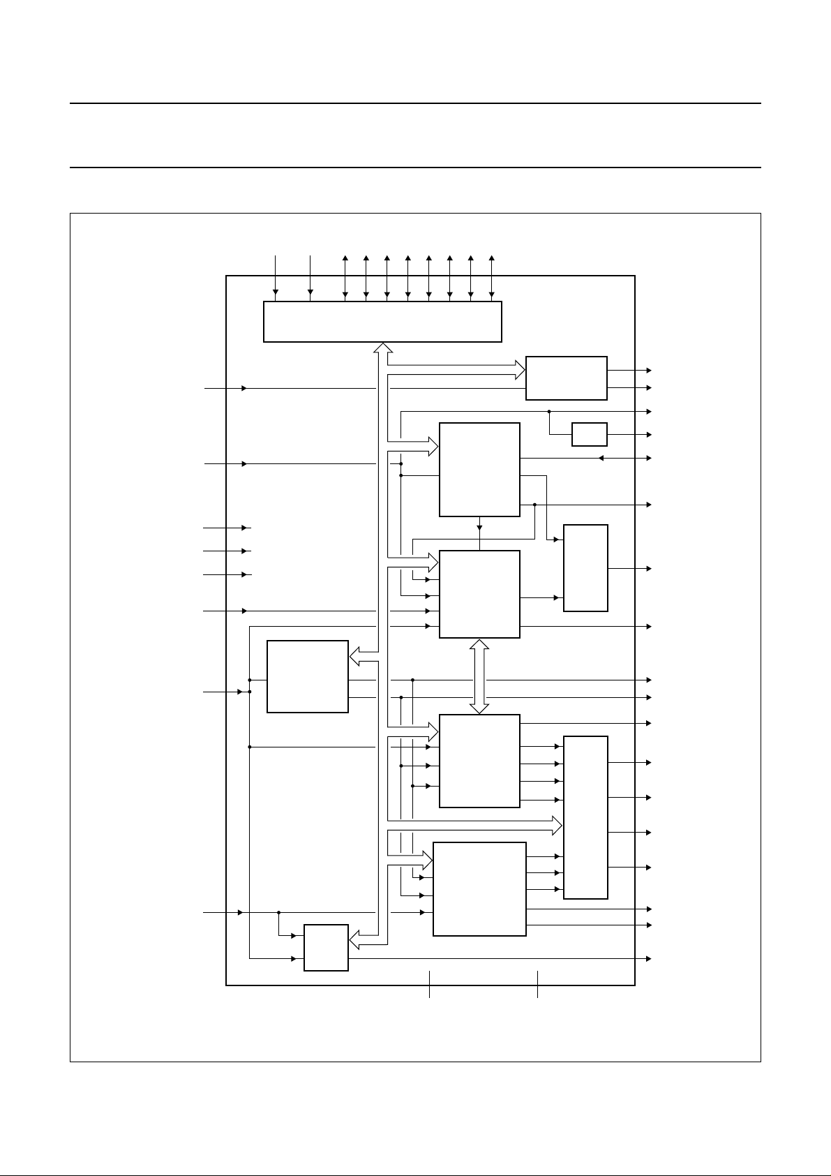
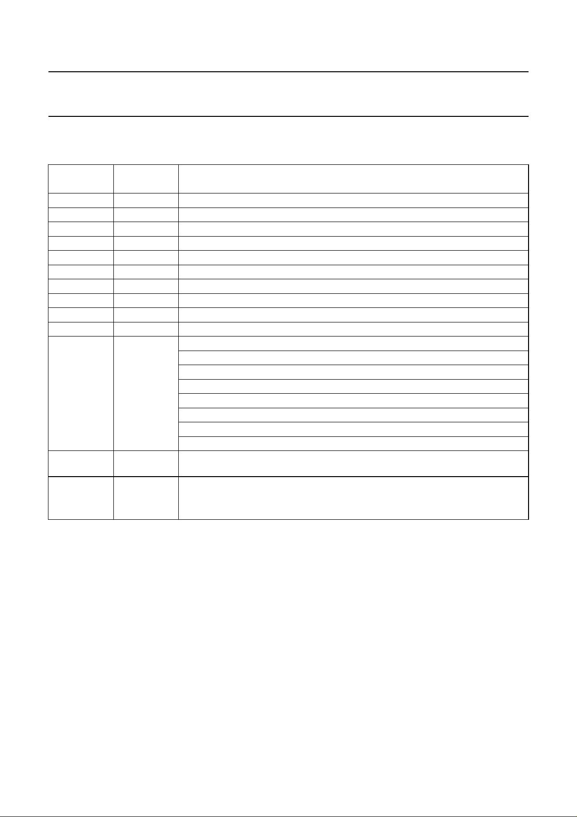
BLOCK DIAGRAM
ALE
handbook, full pagewidth
WRD P0 P1 P2
21 22 25 26 27 28 29 30 31 32
P3 P4 P5 P6 P7
STROBE
LLA
(12, 13.5, 16, 18 MHz)
TEST
SDP
SSC
VACQ
(50/60 Hz)
LLDFL
(27, 32, 36 MHz)
LLD
(32, 36 MHz)
MICROCONTROLLER
INTERFACE
9
13
40
5
41
39
DEFLECTION
33
43
TIMING
LOGIC
ACQUISITION
HORIZONTAL
TIMING
VACQS
ACQUISITION
VERTICAL
TIMING
DISPLAY
VERTICAL
TIMING
DISPLAY
HORIZONTAL
TIMING
2, 10, 23, 36
SAA4952WP
IE
PROCESSING
HWE1
VWE1
VWE2
VRE1
VRE2
VD
HWE2
HRE
HD
12, 24, 34, 44
÷ 2
LOGIC
LOGIC
14
11
16
42
35
37
38
15
17
18
19
20
7
3
6
8
1
4
IE1
IE2
SWC1
SWC05
HRA/BLNA
CLV
WE1
RSTW1
HRDFL
HDFL
VDFL
WE2
HVCD
RE1
RE2
BLND
HRD
SRC
V
DD1
Fig.1 Block diagram.
1997 Jun 10 3
to V
DD4
V
SS1
to V
SS4
MHA724
Philips Semiconductors Objective specification
Memory controller SAA4952WP
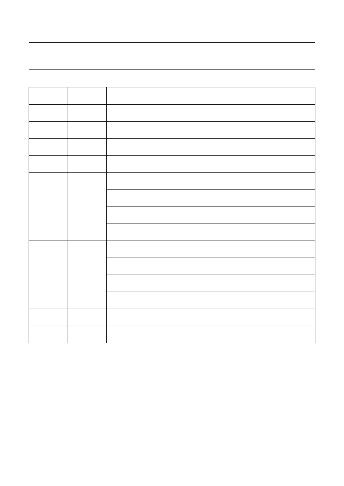
PINNING
SYMBOL PIN I/O DESCRIPTION
HRD 1 O horizontal reference signal output (display PLL)
V
DD1
SWC1 3 O serial write clock output for memory 1
SRC 4 O serial read clock output
SDP 5 I select deflection processor input
SWC05 6 O serial write clock output, SWC1 divided-by-2
IE1 7 O input enable signal output (memory 1)
WE1 8 O write enable signal output (memory 1)
STROBE 9 I strobe signal input
V
DD2
HRA/BLNA 11 I/O horizontal reference signal output (acquisition part)/horizontal blanking
V
SS1
LLA 13 I line-locked clock signal input (acquisition part)
IE2 14 O input enable signal output (memory 2)
WE2 15 O write enable signal output (memory 2)
CLV 16 O horizontal signal output (acquisition part)
HVCD 17 O horizontal, vertical or composite blanking signal output (display part)
RE1 18 O read enable signal output (memory 1)
RE2 19 O read enable signal output (memory 2)
BLND 20 O horizontal blanking signal output (display part)
ALE 21 I address latch enable signal input
WRD 22 I write/read data signal input
V
DD3
V
SS2
P0 25 I/O data input/output signal bit 0
P1 26 I/O data input/output signal bit 1
P2 27 I/O data input/output signal bit 2
P3 28 I/O data input/output signal bit 3
P4 29 I/O data input/output signal bit 4
P5 30 I/O data input/output signal bit 5
P6 31 I/O data input/output signal bit 6
P7 32 I/O data input/output signal bit 7 (MSB = Most Significant Bit)
LLDFL 33 I line-locked clock signal input (deflection part)
V
SS3
HRDFL 35 O horizontal reference signal output (deflection part)
V
DD4
HDFL 37 O horizontal synchronization signal output (deflection part)
VDFL 38 O vertical synchronization signal output (deflection part)
VACQ 39 I vertical synchronization signal input (acquisition part)
2 supply supply voltage 1
10 supply supply voltage 2
signal input, reset for horizontal acquisition counters (acquisition part)
12 − ground 1
23 supply supply voltage 3
24 − ground 2
34 − ground 3
36 supply supply voltage 4
1997 Jun 10 4
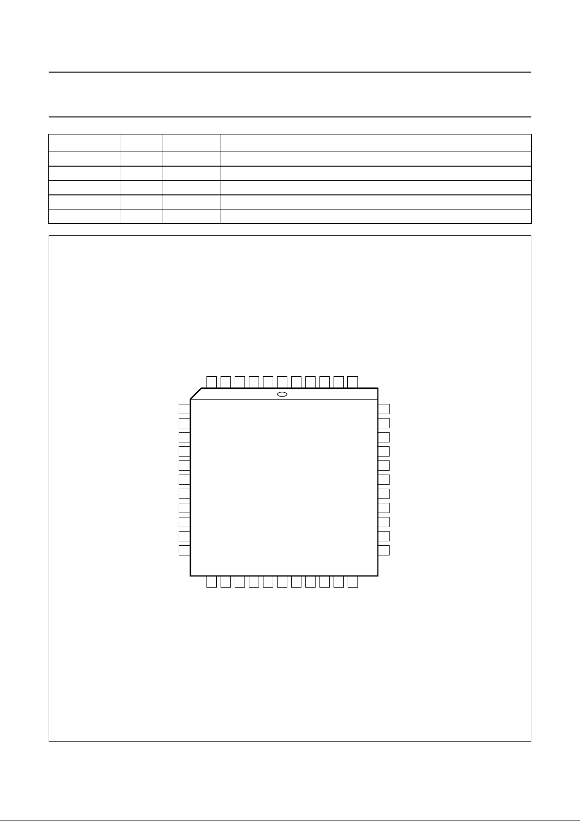
Philips Semiconductors Objective specification
Memory controller SAA4952WP
SYMBOL PIN I/O DESCRIPTION
TEST 40 I test input
SSC 41 I select single clock system input
RSTW1 42 O reset write signal output (memory 1)
LLD 43 I line-locked clock signal input (display part)
V
SS4
44 − ground 4
handbook, full pagewidth
IE1
WE1
STROBE
V
DD2
HRA/BLNA
V
SS1
LLA
IE2
WE2
CLV
HVCD
SS4
SDP
5
19
RE2
SWC1
SRC
4
3
SAA4952WP
21
20
ALE
BLND
V
2
22
WRD
SWC05
6
7
8
9
10
11
12
13
14
15
16
17
18
RE1
DD1
HRD
1
23
DD3
V
V
44
24
SS2
V
LLD
43
25
P0
RSTW1
SSC
42
41
27
26
P1
P2
TEST
40
28
P3
39
38
37
36
35
34
33
32
31
30
29
MHA723
VACQ
VDFL
HDFL
V
DD4
HRDFL
V
SS3
LLDFL
P7
P6
P5
P4
Fig.2 Pin configuration.
1997 Jun 10 5

Philips Semiconductors Objective specification
Memory controller SAA4952WP
FUNCTIONAL DESCRIPTION
The SAA4952WP is a memory controller intended to be
used for scan conversion in TV receivers. This conversion
is performed from 50 to 100 Hz or from 60 to 120 Hz.
Besides the doubling of the field frequency a progressive
scan conversion can be activated (50 Hz/1250 lines or
60 Hz/1050 lines). For low cost PALplus receivers a
simple 50 Hz/1fH mode can be performed. The device
supports up to three separate PLL circuits. The acquisition
PLL can operate with frequencies of 12, 13.5, 16 or
18 MHz. In a three-clock system the deflection PLL
operates with 27 MHz (see Fig.11). An additional display
PLL generates 32 or 36 MHz. If a two-clock system is
chosen the deflection PLL can operate with all possible
display frequencies (27, 32 and 36 MHz) and the extra
PLL can be omitted (see Fig.12). In a system using the
deflection processor TDA9151, three PLLs are necessary
because the 27 MHz clock is needed for the deflection.
If other deflection processors are used (e.g. TDA9152) two
PLLs are sufficient. The 50 Hz/1f
single clock.
Frequency doubling is possible for input data rates of
12, 13.5, 16 and 18 MHz. Displaying a 4 : 3 picture on a
16 : 9 screen is possible by using the clock configuration
12/32 MHz and 13.5/36 MHz. A 14 : 9 picture can be
displayed on a 16 : 9 screen by the frequency
combinations 16/36 MHz or 12/32 MHz. The VCO and
loop filter are peripheral parts of each PLL, the clock
divider and generation of the reference pulse for the phase
detector are internally provided.
The device generates all write, read and clock pulses to
control a field memory in the desired mode. The required
signals are programmable via an 8-bit parallel
microcontroller port.
Figure 1 shows the block diagram of the SAA4952WP.
The clock signal LLA from the VCO is input at pin 13, a
horizontal reference pulse HRA for the phase discriminator
is output at pin 11. By setting the clock divider to different
values the PLL can be forced to operate with different
clock frequencies. The acquisition part can also be
configured to operate with an external clock frequency
from a digital source. Pin 11 is used as an input pin.
The horizontal reference pulse BLNA is supplied externally
to reset the horizontal counters. This mode is intended to
be used together with, for example, a digital colour
decoder which provides the clock and reference pulses.
The signals HWE1, CLV and HVACQS are generated in
the horizontal acquisition processing part. The vertical
processing block supplies the signals RSTW1 as well as a
vertical enable signal (VWE1) for the combined write
mode operates with a
H
enable signal with a horizontal and vertical part (WE1).
The START and STOP position of the pulses are
programmable, whereas the increment equals 2 (4) clock
cycles in the horizontal part and 1 line in the vertical part.
For HWE1 an additional 2-bit fine delay is available.
Display related control signals are derived from the display
clock. The functions are similar to the acquisition part.
The clock frequency can be switched to 27, 32 or 36 MHz.
In the event of a three-clock system using the TDA9151
the 27 MHz clock frequency is generated by an additional
deflection PLL. In the horizontal part the pulses HWE2,
HR2, HD and BLND are programmable in increments of
2 (4) clock cycles, each one adjustable by an additional
2-bit fine delay. The vertical processing block generates
VDFL and enable signals for the horizontal part (VWE2,
VRE1, VRE2 and VD).
The 16 kHz PLL reference pulse HRDFL is generated from
the display clock frequencies (27, 32 or 36 MHz) and the
32 kHz deflection pulse HDFL. In the three-clock system
the deflection pulses are derived from an extra 27 MHz
clock, independent of the chosen mode of the scan
converter module.
The field length of two successive fields is measured in the
vertical acquisition part. The sampling of VACQ is
performed internally via the signal HVACQS, a pulse
which occurs every 32 µs. The position of this pulse is
programmable via the microcontroller interface to ensure
correct sampling of VACQ.
The measured length of the fields can be read by the
microcontroller. Depending on these values the
microcontroller selects an appropriate setting to achieve
an optimized display performance.
The 100 Hz vertical synchronizing signal VDFL is
generated in accordance with the measured length of the
incoming fields. The position towards the video data of this
pulse can also be selected by the microcontroller.
Furthermore two field identification signals for 50 Hz and
for 100 Hz are generated internally to mark the
corresponding display fields for the microcontroller.
The SAA4952WP supports two different Multi
Picture-In-Picture (MPIP) modes. In addition to the
features of the SAA4951WP the new controller is able to
generate a 3 × 3 MPIP without an external PIP module.
The PIP is obtained in a simple way by storing each third
pixel and line of the source into the memory. The display
is able to run free and is not synchronized to the PIP
source in this mode. One of the nine MPIPs can show a
live picture while the others are frozen.
1997 Jun 10 6

Philips Semiconductors Objective specification
Memory controller SAA4952WP
By changing the active MPIP in a sequence all PIPs are
sequentially updated.
The second Multi-PIP option needs an extra PIP module.
This module produces a PIP picture which is originally
displayed at the bottom right position of the screen.
The information of the PIP picture is stored at a desired
position in the field memories. Depending on the
compression mode of the PIP module, the MPIP display
can be configured via software control
(e.g. 4 × 3, 4 × 4, etc.).
For basic features and PALplus systems a 50 Hz/1f
single clock mode is provided. Switching between a 2f
H
H
and the 1fH mode is performed by the SAA4952WP
hardware pin SHF to avoid wrong HDFL frequencies
which might occur in the event of a software controlled
selection. For the same reason the deflection processor is
selected via pin SDP, whereas in the case of the TDA9152
or another deflection processor without the need of a
constant 27 MHz clock, only two PLLs are necessary.
ICs from the new IC generation such as PALplus,
LIMERIC and PAN-IC need to be supplied with two clocks.
The frequency of one clock equals the frequency of the
output data (13.5, 16 or 18 MHz). A second clock operates
with twice the frequency (27, 32 or 36 MHz).
The SAA4952WP generates the necessary signals,
whereas SWC05 is obtained by dividing LLA by a factor of
two.
The display section can be set into a fixed mode via the
microcontroller port. This allows a generator mode
function for displaying OSD without a stable input signal.
A still picture can be shown on the screen completely
decoupled from the input of the converter. The generator
mode can also be used if the MPIP function is activated.
Microcontroller interface
The SAA4952WP is connected to a microcontroller via
pins P0 to P7, ALE and WRD. This controller receives
commands from the I
2
C-bus and sets the register of the
SAA4952WP accordingly. Figure 3 shows the timing of
these signals. Address and data are transmitted
sequentially on the bus with the falling edge of ALE
denoting a valid address and the falling edge of WRD
denoting valid data. The individual registers, their address
and their function are listed in Tables 1 to 12. Various
START and STOP registers are 9 bits wide, in this
instance the MSB is combined with MSBs of other signals
or fine delay control bits in an extra control register which
has to be addressed and loaded separately.
In order to load the proper values to the vertical control
registers (VWE2, VRE1 and VRE2) in the event of e.g.
median filtering, information about the current 100 Hz field
is necessary. To obtain this data, the microcontroller
sends the address 80H (read mode) which puts the
SAA4952WP in output mode for the next address/data
cycle. For this one cycle the WRD pin works as a RDN pin.
The microcontroller is able to read the length of the
incoming fields. The length is measured in multiples of
32 µs. The result of the measurement is a 10-bit data
word. The first 8 bits can be accessed under read address
81H. Register 80H contains the MSB and the 9th bit.
The exact knowledge of the field length makes it possible
to decide in which standard the input signal was
transmitted. The microcontroller is able to detect
non-standard sources such as a VCR in trick modes. It is
also possible to decide whether the input is interlaced or
non-interlaced. The vertical control signals to the
memories are adapted to the source to obtain a stable
display.
handbook, full pagewidth
ALE
WRD
DATA
ADDRESS
DATA
ADDRESS
Fig.3 Microcontroller interface timing.
1997 Jun 10 7
DATA
ADDRESS
MGH133
Philips Semiconductors Objective specification
Memory controller SAA4952WP
Internal registers
Table 1 Vertical display related pulses
ADDRESS
(HEX)
REGISTER FUNCTION
40 VDFLSTA
41 VDFLSTO
42 VWE2STA
43 VWE2STO
44 VRE2STA
45 VRE2STO
46 VRE1STA
47 VRE1STO
53 VDSTA
54 VDSTO
55 VDMSB
62 SETFIELD1
63 SETFIELD2
(1)
start of VDFL pulse (only 8-bit)
(1)
stop of VDFL pulse (only 8-bit)
(2)
start of vertical write enable 2 (lower 8 of 9 bits)
(2)
stop of vertical write enable 2 (lower 8 of 9 bits)
(2)
start of vertical read enable 2 (lower 8 of 9 bits)
(2)
stop of vertical read enable 2 (lower 8 of 9 bits)
(2)
start of vertical read enable 1 (lower 8 of 9 bits)
(2)
stop of vertical read enable 1 (lower 8 of 9 bits)
(2)
start of vertical display signal (lower 8 of 9 bits)
(2)
stop of vertical display signal (lower 8 of 9 bits)
(2)
bit 0: MSB of VRE1STA
bit 1: MSB of VRE1STO
bit 2: MSB of VWE2STA
bit 3: MSB of VWE2STO
bit 4: MSB of VRE2STA
bit 5: MSB of VRE2STO
bit 6: MSB of VDSTA
bit 7: MSB of VDSTO
(1)
field length to be set by the microcontroller in the generator mode (lower 8 of 10 bits);
bit 0 = LSB
(1)
field length to be set by the microcontroller in the generator mode;
bit 0: bit 8 of field length
bit 1: bit 9 of field length (MSB)
Notes
1. VDFLSTA, VDFLSTO, SETFIELD1 and SETFIELD2 are programmable in increments of half lines (16 µs/32 µs).
2. The memory control signals VWE2, VRE1 and VRE2 as well as VD can be changed in steps of one display line.
1997 Jun 10 8
Philips Semiconductors Objective specification
Memory controller SAA4952WP
Table 2 Horizontal display related pulses
ADDRESS
(HEX)
48 BLNDSTA start of horizontal blanking pulse (lower 8 of 9 bits)
49 BLNDSTO stop of horizontal blanking pulse (lower 8 of 9 bits)
4A HWE2STA start of horizontal write enable 2 (lower 8 of 9 bits)
4B HWE2STO stop of horizontal write enable 2 (lower 8 of 9 bits)
4C HRESTA start of horizontal read enable (lower 8 of 9 bits)
4D HRESTO stop of horizontal read enable (lower 8 of 9 bits)
56 HDSTA start of horizontal display signal HD (lower 8 of 9 bits)
57 HDSTO stop of horizontal display signal HD (lower 8 of 9 bits)
4E HDMSB bit 0: MSB of BLNDSTA
4F HDDEL bit 0: fine delay of BLND (LSB)
64 HVSP1 horizontal pulse 1 for frame synchronization, 8-bit resolution
65 HVSP2 horizontal pulse 2 for frame synchronization, 8-bit resolution
66 HVSP3 horizontal pulse 3 for frame synchronization, 8-bit resolution
67 HVSP4 horizontal pulse 4 for frame synchronization, 8-bit resolution
REGISTER FUNCTION
bit 1: MSB of BLNDSTO
bit 2: MSB of HWE2STA
bit 3: MSB of HWE2STO
bit 4: MSB of HRESTA
bit 5: MSB of HRESTO
bit 6: MSB of HDSTA
bit 7: MSB of HDSTO
bit 1: fine delay of BLND (MSB)
bit 2: fine delay of HWE2 (LSB)
bit 3: fine delay of HWE2 (MSB)
bit 4: fine delay of HRE (LSB)
bit 5: fine delay of HRE (MSB)
bit 6: fine delay of HD (LSB)
bit 7: fine delay of HD (MSB)
1997 Jun 10 9

Philips Semiconductors Objective specification
Memory controller SAA4952WP
Table 3 Vertical acquisition related pulses
ADDRESS
(HEX)
50 VWE1STA
51 VWE1STO
52 VAMSB bit 0: MSB of VWE1STA
REGISTER FUNCTION
(1)
start of vertical write enable (lower 8 of 9 bits)
(1)
stop of vertical write enable (lower 8 of 9 bits)
bit 1: MSB of VWE1STO
bit 2:
BRE = 0: normal operation
BRE = 1: RE output is blanking every second line in program scan mode
bit 3:
BWE = 0: normal operation
BWE = 1: WE2 output is blanking every second line in program scan mode
bit 4: BPRR: Blanking Phase Relation RE for program
BPRR = 0: AND connection HRDFL and HRE
BPRR = 1: AND connection HRDFLN and HRE
bit 5: BPRW: Blanking Phase Relation WE2 for program
BPRW = 0: AND connection HRDFL and HWE2
BPRW = 1: AND connection HRDFLN and HWE2
bit 6: BVRA: Blanking Vertical Reset Acquisition
BVRA = 0: reset blanking disabled
BVRA = 1: reset blanking enabled
bit 7: BVRD: Blanking Vertical Reset Display
BVRD = 0: reset blanking disabled
BVRD = 1: reset blanking enabled
Note
1. VWE1 programmable in steps of 1 line (64 µs).
1997 Jun 10 10
 Loading...