

Philips SAA4951WP Datasheet

INTEGRATED CIRCUITS
DATA SH EET
SAA4951
Memory controller
Preliminary specification
File under Integrated Circuits, IC02
April 1994
Philips Semiconductors Preliminary specification
Memory controller SAA4951
FEATURES
• Support for acquisition, display and deflection PLL
• 50/100 (or 60/120) Hz scan conversion for different input
data rates: 12, 13.5, 16 and 18 MHz
• Support for 4:3 and 14:9 display on a 16:9 screen
(horizontal compression)
• Support for Y:U:V data rates of 4:1:1, 4:2:2, and 4:4:4
• Horizontal zoom
• Still picture
• Support for one or two field memories
• Support for different video memory types like
TMS 1050/60/70/2970
GENERAL DESCRIPTION
The memory controller SAA4951 has been designed for
high end TV sets using 2fH-technics.
The circuit provides all necessary write, read and clock
pulses to control different field memory concepts.
Furthermore the drive signals for the horizontal and
vertical deflection power stages are generated.
The device is connected to a microcontroller via an 8-bit
data bus. The controller receives commands via the
I2C-bus. Due to this fact the start and stop conditions of the
main output control signals are programmable and the
SAA4951 can be set in different function modes
depending on the used TV-feature concept.
• Progressive scan
• Programmable via microcontroller port
• Golden Scart option
• Support for Multi-PIP.
QUICK REFERENCE DATA
SYMBOL PARAMETER MIN. TYP. MAX. UNIT
V
DD
I
DD
T
amb
supply voltage 4.5 5.0 5.5 V
supply current − 50 − mA
operating ambient
0 − +70 °C
temperature
ORDERING INFORMATION
EXTENDED
TYPE NUMBER
PINS
PIN
POSITION
SAA4951WP 44 PLCC plastic SOT187
Note
1. SOT187-2; 1996 December 13.
April 1994 2
PACKAGE
MATERIAL CODE
(1)

Philips Semiconductors Preliminary specification
Memory controller SAA4951
Y/U/V
BENDIC
SAA7158
12
NORIC
SAA4940
1212
MEMORY 1
1 × TMS4C2970
(3 × TMS4C1070)
VIDEO
REDUCTION
LINEFLICKER
ENHANCEMENT
NOISE
INCLUSIVE
REDUCTION
MEMORY 2
A/D
TDA8755
2
DACs
12
2
REDUCTION
CROSSCOLOUR
12
1 × TMS4C2970
(3 × TMS4C1070)
12
VCO2
12/13.5/16/18 MHz CONTROL 32/36 MHz
VCO1
H2, V2
(32 kHz/100 Hz)
SAA4951
MEMORY
CONTROLLER
2
27 MHz
VCO2B
µC-BUS
µC
28
MGH131
PCB83C652
Fig.1 Improved Picture Quality (IPQ) module.
LPY
Y
handbook, full pagewidth
LPU
U
LPV
V
April 1994 3
SYNC
V
SCI
C
2
I
Philips Semiconductors Preliminary specification
Memory controller SAA4951
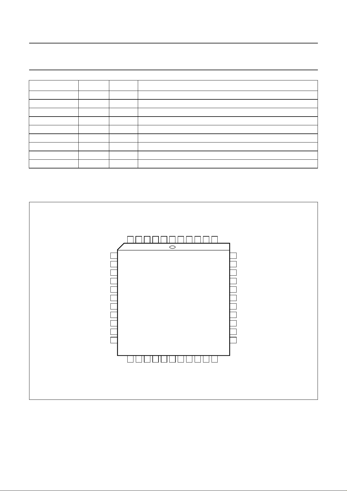
PINNING
SYMBOL PIN TYPE
(1)
DESCRIPTION
HRD 1 O horizontal reference signal, display part
V
DD
2 − positive supply voltage
SWC1 3 O serial write clock, memory 1
SRC 4 O serial read clock, memory 1
SWC2 5 O serial write clock, memory 2
WEXT 6 I external write enable input
IE1 7 O input enable signal, memory 1
WE1 8 O write enable signal, memory 1
STROBE 9 I strobe function
V
DD
10 − positive supply voltage
HRA 11 O horizontal reference signal, acquisition part
BLNA I horizontal blanking signal, acquisition part
V
SS
12 − ground
LLA 13 I line-locked clock signal, acquisition part
IE2 14 O input enable signal, memory 2
WE2 15 O write enable signal, memory 2
CLV 16 O video clamping signal
ALDUV/VB 17 O acquisition load signal, chrominance U, V / vertical blanking
RE1 18 O read enable signal, memory 1
RE2 19 O read enable signal, memory 2
BLND 20 O horizontal blanking signal, display part
ALE 21 I address latch enable signal
WRD 22 I write/read data signal
V
DD
V
SS
23 − positive supply voltage
24 − ground
P0 25 I data input signal, (LSB = least significant bit)
P1 26 I data input signal
P2 27 I data input signal
P3 28 I data input signal
P4 29 I data input signal
P5 30 I data input signal
P6 31 I/O data input/output signal
P7 32 I/O data input/output signal, (MSB = most significant bit)
LLDFL 33 I line-locked clock signal, deflection part
V
SS
34 − ground
HRDFL 35 O horizontal reference signal, deflection part
April 1994 4
Philips Semiconductors Preliminary specification
Memory controller SAA4951
SYMBOL PIN TYPE
V
DD
36 − positive supply voltage
(1)
DESCRIPTION
HDFL 37 O horizontal synchronization signal, deflection part
VDFL 38 O vertical synchronization signal, deflection part
VACQ 39 I vertical synchronization signal, acquisition part
TEST 40 I test input
RSTW2 41 O reset write signal, memory 2
RSTW1 42 O reset write signal, memory 1
LLD 43 I line-locked clock signal, display part
V
SS
44 − ground
Note
1. I = Input
O = Output
handbook, full pagewidth
SS
WEXT
6
SWC2
5
SRC
4
SWC1
3
DD
V
2
HRD
1
LLD
V
44
43
RSTW1
RSTW2
42
41
TEST
40
IE1
WE1
STROBE
V
DD
HRA/BLNA
V
SS
LLA
IE2
WE2
CLV
ALDUV/VB
7
8
9
10
11
12
13
14
15
16
17
18
19
RE1
RE2
SAA4951WP
21
20
ALE
BLND
22
WRD
25
P0
26
P1
27
P2
23
24
SS
DD
V
V
28
P3
39
38
37
36
35
34
33
32
31
30
29
MGH129
VACQ
VDFL
HDFL
V
DD
HRDFL
V
SS
LLDFL
P7
P6
P5
P4
Fig.2 Pin configuration.
April 1994 5

Philips Semiconductors Preliminary specification
Memory controller SAA4951
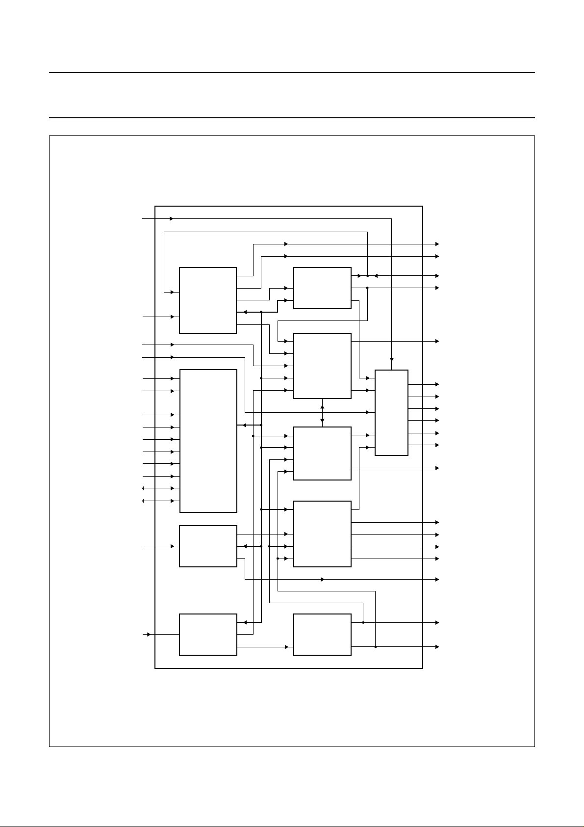
FUNCTIONAL DESCRIPTION
Block diagram and short description
The SAA4951 is a memory controller intended to be used
for scan conversion in TV receivers. This conversion is
done from 50 to 100 Hz or from 60 to 120 Hz. The device
supports three separate PLL circuits: the acquisition PLL
can run on 12, 13.5, 16 or 18 MHz, the display PLL on 27,
32 or 36 MHz, and the deflection PLL on 27 MHz. This
allows frequency doubling for input data rates of 13.5, 16
and 18 MHz. For displaying a 4:3 picture on a 16:9 screen
additional horizontal compression is possible when using
the clock configuration 12/32 MHz and 13.5/36 MHz. The
VCO and loop filter are peripheral parts of each PLL, the
clock divider and generation of the reference pulse for the
phase detector are internally provided.
The device generates all write, read and clock pulses to
operate a field memory in a desired mode. The required
signals are programmable via an 8-bit parallel
microcontroller port.
The block diagram of the SAA4951 is shown in Fig.3. The
clock signal from the VCO is fed in at pin 13, a horizontal
reference pulse for the phase discriminator is fed out at
pin 11.
By setting the clock divider to different values the PLL can
be forced to run on different clock frequencies.
Besides this the acquisition part can also be configured to
run on a fixed input clock. Then pin 11 is an input pin, so
the horizontal reference pulse can be supplied from the
outside. This mode is intended to be used together with a
digital decoder which is providing clock and reference
pulses.
In the horizontal processing part the signals WE1, WE2
and CLV are generated. The vertical processing block
supplies the signals RSTW1 and RSTW2 as well as
enable signals for the horizontal part. The start and stop
position of the pulses are programmable, the increment
being 4 clock cycles in the horizontal part and 1 line in the
vertical part. For WE1 and WE2 an additional 2-bit fine
delay is available.
Display related control signals are derived from the display
PLL. The functions are similar to the acquisition part. The
PLL can be switched to 32 or 36 MHz, in case of 27 MHz
this clock is taken from the deflection PLL which always
runs on 27 MHz. In the horizontal part the pulse WE2,
RE1, RE2 and BLN are programmable in increments of 4
clock cycles, each one adjustable by an additional 2-bit
fine delay. The vertical processing block generates VDFL,
RSTW2 and enable signals for the horizontal part.
The deflection PLL runs on 27 MHz. From this clock the
16 kHz PLL reference pulse HRDFL is generated as well
as the 32 kHz deflection pulse HDFL.
In the vertical acquisition part the distance between the
incoming 50 Hz vertical synchronization pulse VACQ and
the horizontal synchronization pulse CLV generated by the
horizontal deflection circuit is measured. In addition the
field length is calculated by the acquisition counter, which
is enabled by CLV.
A fixed vertical reset pulse RSTW1 and a programmable
vertical control of the write enable pulse WE1 for
memory 1 defining the vertical write window are
generated.
In the display section the programmable 100 Hz write
enable pulse WE2 for the memory 2 and the
programmable 100 Hz read enable pulses RE1 and RE2
are provided. The 100 Hz vertical synchronizing signal
VDFL is corrected by the calculated values of the
acquisition part. The position of this pulse can also be
chosen by the microcontroller. Furthermore two field
identification signals for 50 Hz and for 100 Hz are
generated internally to mark the corresponding fields by
the microcontroller.
April 1994 6
Philips Semiconductors Preliminary specification
Memory controller SAA4951
handbook, full pagewidth
WEXT
LLA
VACQ
STROBE
ALE
WRD
P0
P1
P2
P3
P4
P5
P6
P7
LLD
6
13
39
9
21
22
25
26
27
28
29
30
31
32
43
SAA4951
ACQ-CLOCK
GENERATOR
MICRO-
PROCESSOR-
INTERFACE
DSP-CLOCK
GENERATOR
ACQ
H-TIMING
ACQ
V-TIMING
DSP
V-TIMING
DSP
H-TIMING
LOGIC
17
ALDUV/VB
3
SWC1
11
HRA/BLNA
16
CLV
42
RSTW1
5
SWC2
41
RSTW2
8
WE1
15
WE2
7
IE1
14
IE2
38
VDFL
20
BLND
18
RE1
19
RE2
1
HRD
4
SRC
LLDFL
33
DFL-CLOCK
GENERATOR
Fig.3 Block diagram.
April 1994 7
DFL
TIMING
37
35
MGH130
HDFL
HRDFL
Philips Semiconductors Preliminary specification
Memory controller SAA4951
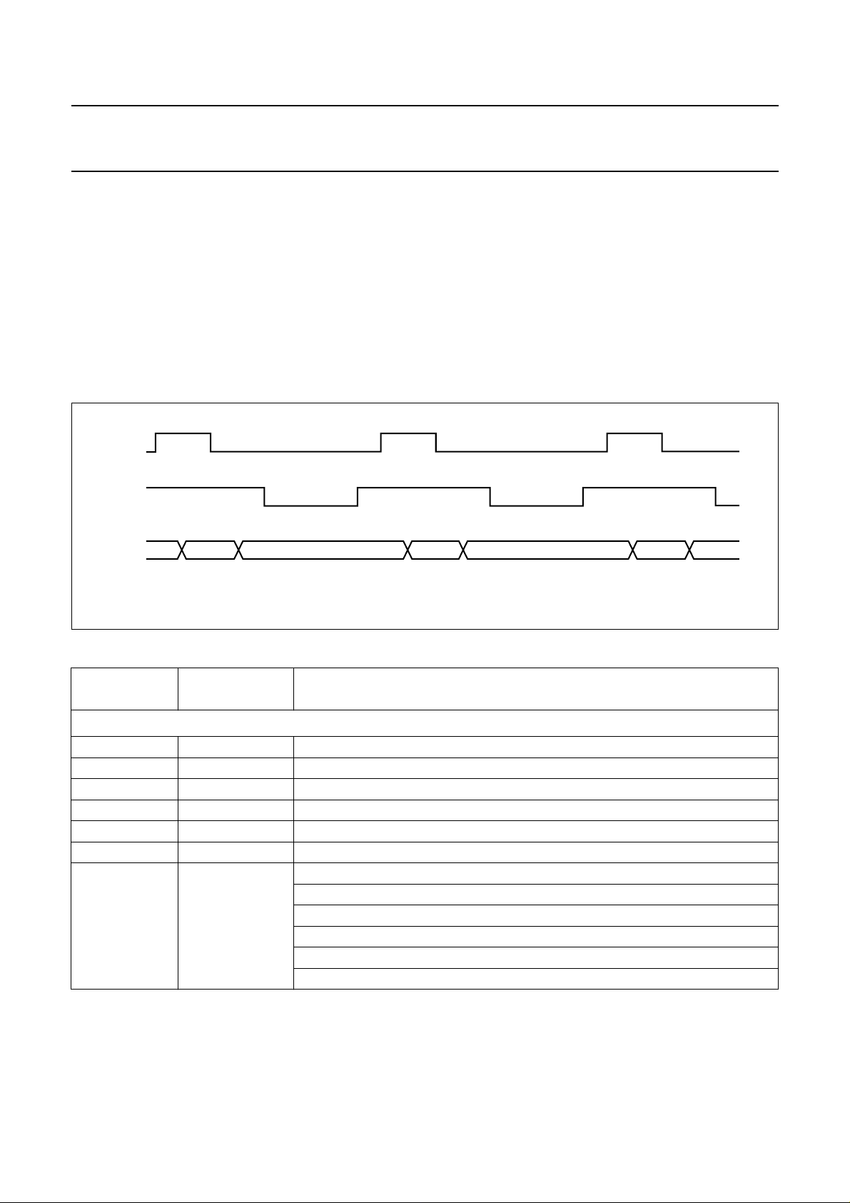
Microcontroller interface
The SAA4951 is connected to a microcontroller via pins P0
to P7, ALE and WRD. This controller receives commands
from the I2C-bus and sets the registers of the
SAA4951 accordingly. Fig.4 shows the timing of these
signals. Address and data are transmitted sequentially on
the bus with the falling edge of ALE denoting a valid
address and the falling edge of WRD indicating valid data.
The individual registers, their address and their function
are listed in Table 1. Various start and stop registers are
handbook, full pagewidth
ALE
WRD
DATA
ADDRESS
DATA
Fig.4 µP-interface timing.
9 bits wide, in this case the MSB is combined with other
MSBs or fine delay control bits in an extra register which
has to be addressed and loaded separately.
In order to load the proper values to the vertical write
enable registers in case of median filtering, information
about the current 100 Hz field is necessary. To obtain
these data, the microcontroller sends the address 80Hex
(READ mode) which puts the SAA4951 in output mode for
the next address / data cycle. For this one cycle the WRD
pin works as a RDN pin.
ADDRESS
DATA
ADDRESS
MGH133
Table 1 Internal registers.
ADDRESS
(HEX)
REGISTER FUNCTION
Vertical pulses generated from the display clock
40 VDFLSTA start of VDFL pulse (lower 8 of 9 bits)
41 VDFLSTO end of VDFL pulse (lower 8 of 9 bits)
42 VWE2STA start of vertical write enable (lower 8 of 9 bits)
43 VWE2STO end of vertical write enable (lower 8 of 9 bits)
44 VRE2STA start of vertical read enable (lower 8 of 9 bits)
45 VRE2STO end of vertical write enable (lower 8 of 9 bits)
46 VDMSB bit 0: MSB of VDFLSTA
bit 1: MSB of VDFLSTO
bit 2: MSB of VWE2STA
bit 3: MSB of VWE2STO
bit 4: MSB of VRE1STA
bit 5: MSB of VRE1STO
April 1994 8
 Loading...