

Philips saa4945h DATASHEETS

INTEGRATED CIRCUITS
DATA SH EET
SAA4945H
LIne MEmory noise Reduction IC
(LIMERIC)
Preliminary specification
File under Integrated Circuits, IC02
1997 Jun 10
Philips Semiconductors Preliminary specification
LIne MEmory noise Reduction IC
(LIMERIC)
FEATURES
• 2-D adaptive vertically recursive noise reduction
• Noise reduction for Y, U and V signals in 4 : 1 : 1 format
• Single 5 V ±10% power supply
• Communication by means of serial communication
protocol 83C654 (SNERT bus)
• Via SNERT bus, 10 different types of noise reduction
selectable; the noise reduction function can also be
disabled
• Phase relation write enable input/output signal
simultaneously switchable over one clock period w.r.t.
input/output samples
• 8-bit wide data processing for Y, U and V; in unsigned
format (Y signal) and in 2’s complement (U and V
signals)
• One fixed line locked clock operation frequency up to
16 MHz (typical)
• Exactly one line delay.
SAA4945H
GENERAL DESCRIPTION
The SAA4945H, LIMERIC (LIne MEmory noise Reduction
IC) is a 2-D recursive noise reduction filter for both
luminance and colour difference signals. The noise
reduction is automatically adapted to the global noise level
in the image. Ten different preferences of noise reduction
can be set using a synchronous receiver transmitter bus;
SNERT (Synchronous No parity Eight bit Receive
Transmit) bus. Alternatively, the noise reduction can be
switched off. The LIMERIC is generally placed directly
after the ADC in the feature box and works fully in the 1f
(50/60 Hz) domain.
h
QUICK REFERENCE DATA
SYMBOL PARAMETER CONDITIONS MIN. TYP. MAX. UNIT
V
DD
I
DD
supply voltage (pins 5, 29 and 30) 4.5 5.0 5.5 V
supply current − 70 − mA
P power dissipation − 350 − mW
f
CLK
f
SNERT
T
amb
clock frequency ±7%; note 1 10 16 17.1 MHz
bus clock frequency −−1 MHz
operating ambient temperature 0 − 70 °C
Note
1. Maximum number of clocks per line is 1024.
ORDERING INFORMATION
TYPE
NUMBER
NAME DESCRIPTION VERSION
PACKAGE
SAA4945H QFP44 plastic quad flat package; 44 leads (lead length 1.3 mm); body 10 × 10 × 1.75 mm SOT307-2
1997 Jun 10 2
Philips Semiconductors Preliminary specification
LIne MEmory noise Reduction IC
(LIMERIC)
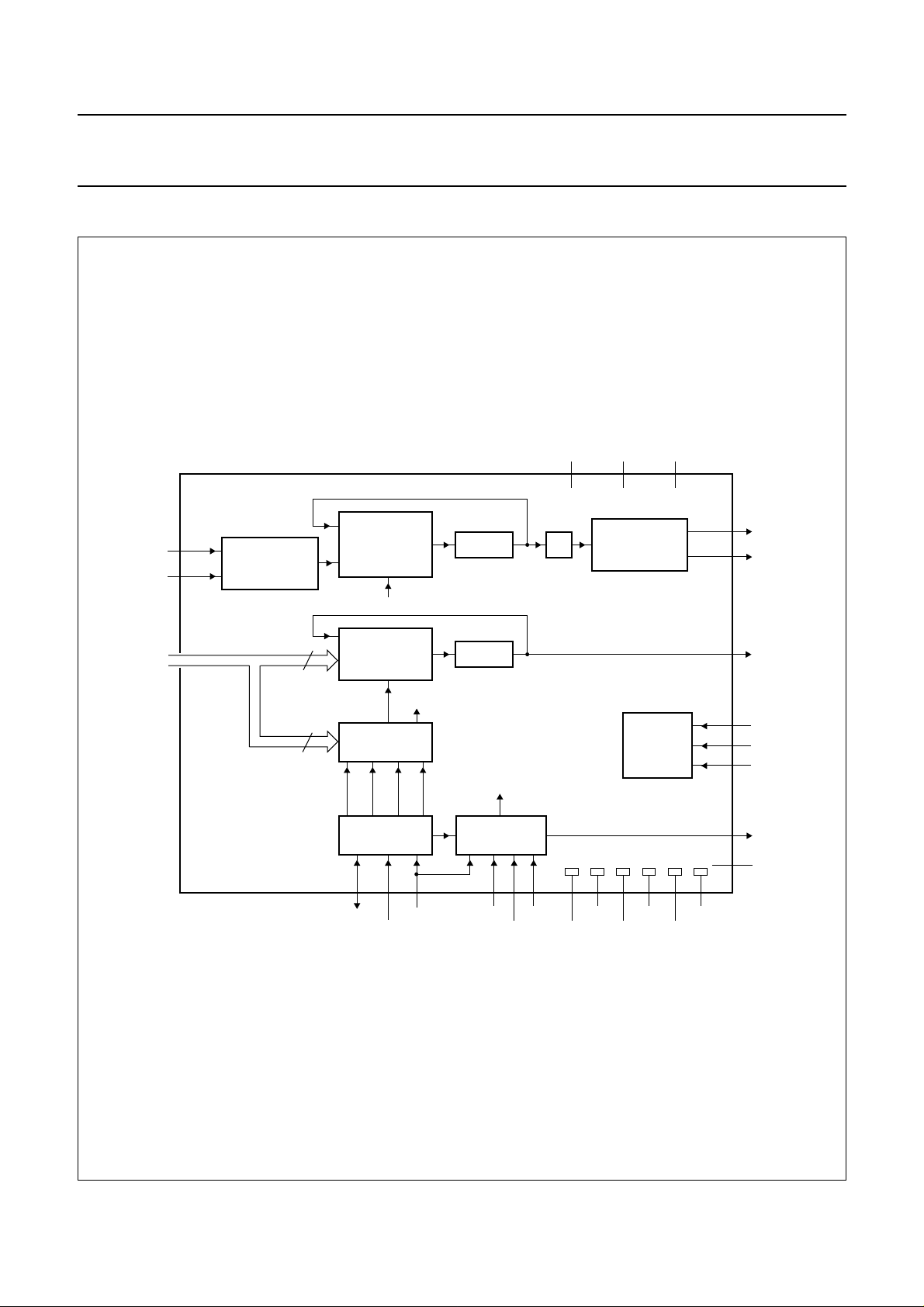
BLOCK DIAGRAM
handbook, full pagewidth
NOISE
UI0, U
VI0, V
16, 15
I1
I1
18, 17
REFORMATTER
REDUCTION
FILTER
(MULTIPLEXED)
N_thr_UV
RAM_UV ∆t
V
DD1
5
V
FORMATTER
DD2
V
29
DD3
SAA4945H
30
36, 37
34, 35
UO0, U
VO0, V
O1
O1
Y
to Y
I0
I7
814 to 7
8
NOISE
REDUCTION
FILTER
N_thr_Y
NOISE
ESTIMATOR
TASTE
NTHR
SNERT
INTERFACE
SDNA
SNCL
N_thr_UV
val
W
YpScale
VRST
RAM_Y
SAA4945H
internal
control
signals
CONTROL
432
2221
19
VaCLK
I
6
GND1WE
20
GND2
23
GND3
TEST
CONTROL
27
GND4
GND5
38 to 44, 1
28
32
GND6
Y
to
O0
YO6, Y
O7
26
TST0
25
TST1
24
TST2
31
WE
O
33
n.c.
MGK170
Fig.1 Block diagram.
1997 Jun 10 3

Philips Semiconductors Preliminary specification
LIne MEmory noise Reduction IC
(LIMERIC)
PINNING
SYMBOL PIN TYPE DESCRIPTION
Y
O7
SNDA 2 input/output data from interface SNERT bus
SNCL 3 input clock from interface SNERT bus
VRST 4 input reset in the vertical blanking interval
V
DD1
GND1 6 ground ground 1
Y
I7
Y
I6
Y
I5
Y
I4
Y
I3
Y
I2
Y
I1
Y
I0
U
I1
U
I0
V
I1
V
I0
CLK 19 input master clock
GND2 20 ground ground 2
WE
I
Va 22 input vertical blanking pulse
GND3 23 ground ground 3
TST2 24 input test pin 2
TST1 25 input test pin 1
TST0 26 input test pin 0
GND4 27 ground ground 4
GND5 28 ground ground 5
V
DD2
V
DD3
WE
O
GND6 32 ground ground 6
n.c. 33 − not connected
V
O0
V
O1
U
O0
U
O1
Y
O0
Y
O1
Y
O2
1 output luminance output bit 7
5 supply supply voltage 1
7 input luminance input bit 7 from analog-to-digital converter
8 input luminance input bit 6 from analog-to-digital converter
9 input luminance input bit 5 from analog-to-digital converter
10 input luminance input bit 4 from analog-to-digital converter
11 input luminance input bit 3 from analog-to-digital converter
12 input luminance input bit 2 from analog-to-digital converter
13 input luminance input bit 1 from analog-to-digital converter
14 input luminance input bit 0 from analog-to-digital converter
15 input U input bit 1 from analog-to-digital converter
16 input U input bit 0 from analog-to-digital converter
17 input V input bit 1 from analog-to-digital converter
18 input V input bit 0 from analog-to-digital converter
21 input write enable input
29 supply supply voltage 2
30 supply supply voltage 3
31 output write enable output
34 output V output bit 0
35 output V output bit 1
36 output U output bit 0
37 output U output bit 1
38 output luminance output bit 0
39 output luminance output bit 1
40 output luminance output bit 2
SAA4945H
1997 Jun 10 4

Philips Semiconductors Preliminary specification
LIne MEmory noise Reduction IC
(LIMERIC)
SYMBOL PIN TYPE DESCRIPTION
Y
O3
Y
O4
Y
O5
Y
O6
handbook, full pagewidth
41 output luminance output bit 3
42 output luminance output bit 4
43 output luminance output bit 5
44 output luminance output bit 6
O1
O6
YO5YO4YO3YO2YO1Y
Y
44
43
42
41
O0
U
40
39
38
37
UO0VO1V
36
35
O0
34
SAA4945H
Y
O7
SNDA
SNCL
VRST
V
DD1
GND1
Y
Y
Y
Y
Y
22
Va
33
32
31
30
29
28
27
26
25
24
23
MGK169
n.c.
GND6
WE
V
DD3
V
DD2
GND5
GND4
TST0
TST1
TST2
GND3
O
1
2
3
4
5
6
7
I7
8
I6
9
I5
10
I4
11
I3
12
13
I2
I1
Y
Y
14
I0
Y
SAA4945H
15
16
I1
I0
U
U
19
CLK
20
GND2
21
I
WE
17
18
I0
I1
V
V
Fig.2 Pin configuration.
1997 Jun 10 5
Philips Semiconductors Preliminary specification
LIne MEmory noise Reduction IC
(LIMERIC)
FUNCTIONAL DESCRIPTION
The digital LIMERIC is an effective low noise reduction IC
for luminance and colour difference signals. Noise filtering
is automatically adapted to the global noise level which is
measured within the picture content. The two dimensional
non-linear noise reduction (one for luminance, one for
chrominance) uses only line memory to function.
Furthermore, up to 10 different preferences can be set by
the user.
As shown in Fig.1, the main components of the device are
the noise reduction filter with the line memories (RAM) and
the noise estimator. Other components shown are the
reformatter, formatter, controller and a SNERT bus
transceiver.
Noise reduction filter
Both luminance and chrominance signals are filtered with
vertical recursion. This is produced as the filter receives
both filtered samples from the previous line, and unfiltered
samples from the current line. A new replacement value is
calculated for each sample read from the line memory.
This in turn, is the filtered response value for the reference
input pixel. The reference pixel is then placed at the centre
of the delay-line into which the current (unfiltered) video
line is shifted. Tables 1 to 6 show this as an ‘O’.
Both luminance and colour difference signals are filtered
using the so-called Discriminating AveragingFilter (DAF),
in which filter coefficients are related to the Absolute
Difference (AD) between samples. The filter uses samples
from both present and previous line (using the line delay)
and the result of the filter is stored back in the line memory.
In this way a vertical recursive structure is realized.
The filter coefficients are set depending on the noise
measured by the noise estimator or the NTHR (SNERT
register F9).
SAA4945H
LUMINANCE FILTER
The taps structure of the luminance filter is as shown in
Table 2.
Table 2 Luminance processing
X . . . . X . . . X . . . X . . . . X ← 5 Y samples from the
filtered line (distance 4 / 5
pixel)
o . O . o ← 3 Y samples from the
incoming line (distance 2
pixels)
A ‘weave’ function is used to reduce any smearing effect
that could occur at edges. As shown in Tables 3 to 6, the
‘weave’ calculates over 4 consecutive lines. The relative
position of the actual pixel changes one position every line.
Table 3 For line 2n
X . . . . X . . . X . . . X . . . . X
o . O . o
Table 4 For line 2n + 1
X . . . . X . . . X . . . X . . . . X
. . o . O . o
Table 5 For line 2n + 2
X . . . . X . . . X . . . X . . . . X
o . O . o
Table 6 For line 2n + 3
X . . . . X . . . X . . . X . . . . X
o . O . o . .
C
HROMINANCE FILTER
The basic signal processing for either U or V is via the
same filter. It is used to process both V and U using a
multiplexed operation.
The taps structure of the chrominance filter is as shown in
Table 1.
Table 1 Chrominance processing
X X X X X ← 5 adjacent R − Y samples from the
filtered line
o O o ← 3 adjacent R − Y samples from the
incoming line
1997 Jun 10 6
Table 7 Weave configuration
Depending on even and odd fields the ‘weave’ has the
following configuration:
ODD FIELDS EVEN FIELDS
XX
XX
XX
XX
XX
XX
XX
 Loading...