

Philips SAA4700T-V5 Datasheet

DATA SH EET
Preliminary specification
File under Integrated Circuits, IC02
March 1991
INTEGRATED CIRCUITS
SAA4700T
VPS dataline processor
March 1991 2
Philips Semiconductors Preliminary specification
VPS dataline processor SAA4700T
FEATURES
• Adaptive sync slicer with buffered composite sync
output VCS
• Adaptive data slicer
• Data rate clock regenerator
• Field selection and line 16 decoding
• Startcode and biphase check
• Data valid output
• Storage of data line information in a 40 bit register bank
• I2C-bus transmission
GENERAL DESCRIPTION
The SAA4700T is a bipolar integrated circuit designed for
use in dataline receivers and incorporates a dataline slicer
and decoder. The slicer extracts the dataline signal from
the video signal and regenerates the data clock. It also
provides signals for the decoder in order to decode the
binary data that is transmitted in line 16 of every first field
of the composite video signal (video programming signal
and video recording programming by Teletext, VPS and
VPT systems). The decoded information out of words 5
and 11 to 14 is accessed via the built-in I2C-bus interface.
This information then can be used for programming a
video cassette recorder in order to start and stop a
recording of a television program at the correct aligned
time, regardless of a delay or extension in the transmission
time of the required program.
QUICK REFERENCE DATA
ORDERING AND PACKAGE INFORMATION
Note
1. SOT163-1; 1996 November 13.
SYMBOL PARAMETER MIN. TYP. MAX. UNIT
V
P
supply voltage (pins 17 and 18) 4.5 5 5.5 V
I
P
total supply current − 18 23 mA
V
i CVBS
CVBS input signal sync-to-white
(peak-to-peak value)
0.5 1 1.4 V
T
amb
operating ambient temperature 0 −+70 °C
EXTENDED
TYPE NUMBER
PACKAGE
PINS PIN POSITION MATERIAL CODE
SAA4700T 20 mini-pack plastic SOT163A
(1)
March 1991 3
Philips Semiconductors Preliminary specification
VPS dataline processor SAA4700T
handbook, full pagewidth
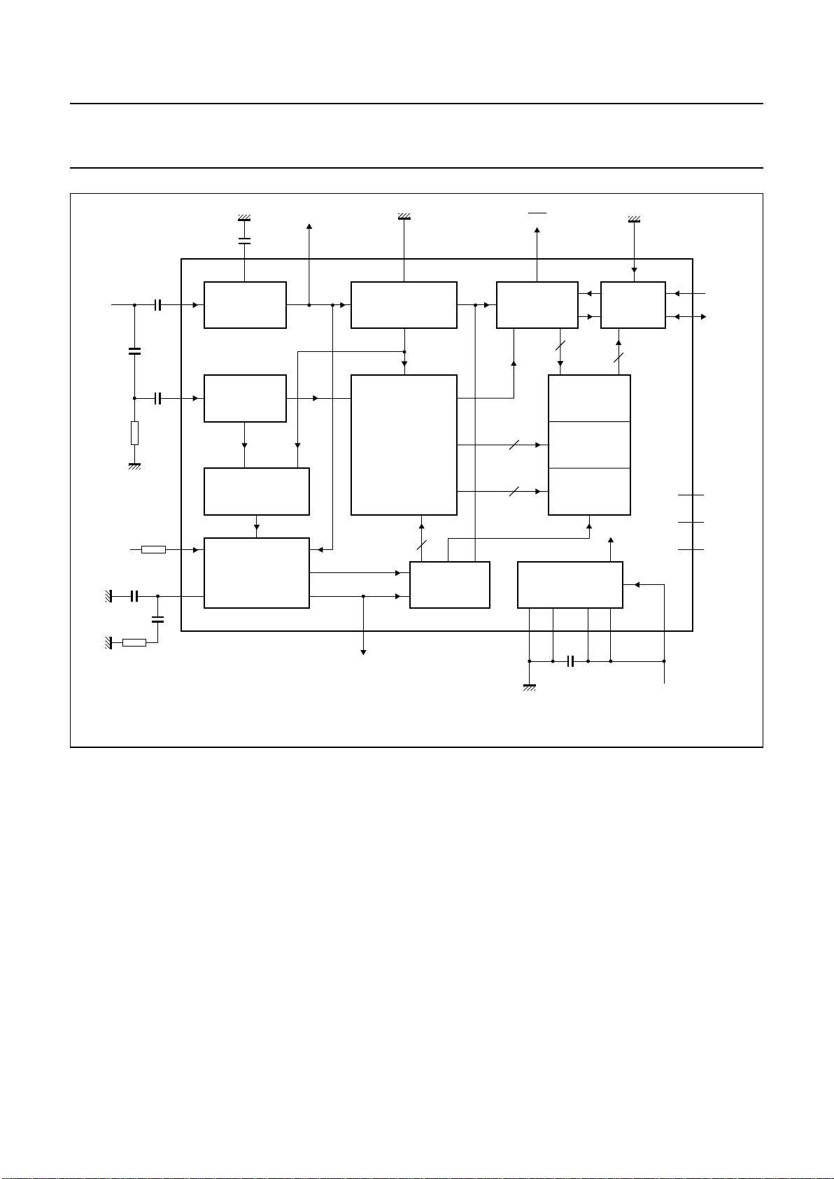
MGH128
8.2 kΩ
0.1 µF
external
reset
V
P
22
nF
SYNC
SEPARATOR
FIELD SELECTOR
LINE 16 DECODER
I2C-BUS
CONTROL
OUTPUT
CONTROLLER
INPUT
CONTROLLER
40 BIT DATA
REGISTER
40 BIT
DATA LATCH
MULTIPLEXER
DATA
SLICER
CLOCK
REGENERATOR
PLL WITH
5 MHz VCO AND
PHASE DETECTOR
TIME BASE
clock pulse
REFERENCE
VOLTAGES
POWER-ON RESET
data
SAA4700T
SCL
n.c.
SDA
4
5
6
8
20
n.c.
14
n.c.
7
10
9
to V
P
75 kΩ
(2%)
4.7
kΩ
CVBS
CSO
4.7 nF
1 nF
(test line 16)
DAV
470 pF
4.7 nF
0.1
µF
2
5 6 12 13 8
AD = LOW
1
15
19
16 3 4 17 18 11
data
VCS
line 16
+5 V
Fig.1 Block diagram and test circuit.
FUNCTIONAL DESCRIPTION
Dataline 16
The information in dataline 16 consists of fifteen 8-bit
words; the total information content is shown in Table 1;
and the organization of transmitted bytes is shown in
Table 2.
Out of the fifteen possible 8-bit words the SAA4700T
extracts words 5 and 11 to 14. The contents of these words
can be read via the built-in I
2
C-bus interface. The circuit is
fully transparent, thus each bit is transferred without
modification with only the sequence of words being
changed. Words 11 to 14 are transmitted first followed by
word 5.
By evaluating the sliced sync signal the circuit can identify
the beginning of dataline 16 in the first field. The dataline
decoder stage releases the start code detector. When a
correct start code is detected (for timing of start code
detection see Fig.3) words 5 and 11 to 14 are decoded,
checked for biphase errors and stored in a register bank. If
no biphase error has occurred, the contents of the register
bank are transferred to a second register bank by the data
valid control signal. If the system has been addressed, this
transfer will be delayed until the next start or stop condition
of the I
2
C-bus has been received.
The last bit of correct information on the dataline remains
available until it is read via the I2C-bus. Once the stored
information has been read it is considered to be no longer
valid and the internal new data flag is reset. Subsequently,
if the circuit is addressed, the only VPS data that will be
sent back is “FFF to F”. The same conditions apply after
power-up when no data can be read out. New data is
available after reception of another error-free dataline 16.
March 1991 4
Philips Semiconductors Preliminary specification
VPS dataline processor SAA4700T
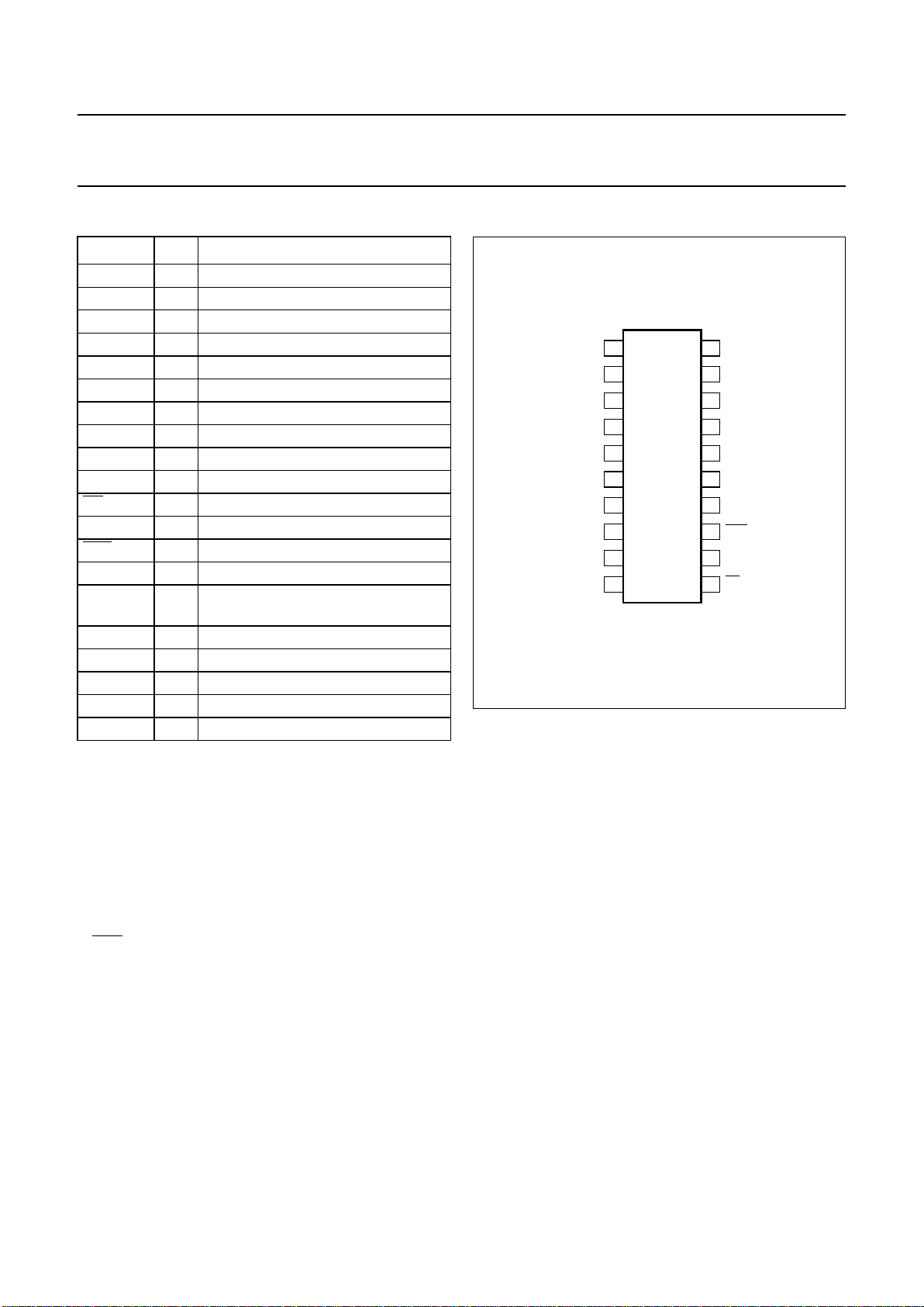
PINNING
SYMBOL PIN DESCRIPTION
CVBS 1 video signal input (CVBS from TV)
SYNC 2 sync amplitude input (CVBS from TV)
GND1 3 analog ground (0 V)
GND2 4 digital ground (0 V)
C
black
5 capacitor for black level
CSO 6 composite sync output
n.c. 7 not connected
AD 8 address set input
SCL 9 I
2
C-bus clock line
SDA 10 I
2
C-bus data line
RS 11 reset input active LOW
TP 12 test point for line 16 decoder
DAV 13 data available output active LOW
n.c. 14 not connected
R
osc
15 oscillator resistor for frequency
adjustment
CP 16 test point clock pulse
V
P1
17 +5 V supply voltage (digital part)
V
P2
18 +5 V supply voltage (analog part)
C
ph
19 capacitor of phase detector
n.c. 20 not connected
PIN CONFIGURATION
Fig.2 Pin configuration.
handbook, halfpage
SAA4700T
MBH797
1
2
3
4
5
6
7
8
9
10
20
19
18
17
16
15
14
13
12
11
CVBS
SYNC
GND1
GND2
CSO
n.c.
AD
SCL
SDA
C
black
n.c.
RS
TP
DAV
CP
n.c.
R
osc
V
P1
V
P2
C
ph
External reset
The circuit provides an internal power-on reset. When
using this facility pin 11 should be connected to VP or, if
external reset (RESET = LOW) is to be used pin 11 should
be prepared by connecting pin 11 via a 10 kΩ pull-up
resistor to VP.
Reset forces the following:
• I2C-bus not to acknowledge
• DAV output to go HIGH (pin 13)
• I2C-bus transfer register to “FFF”
CVBS input
The CVBS signal is applied to the sync separator (pin 2)
via a decoupling capacitor and to the data slicer (pin 1) via
an RC high-pass filter. To enable proper storage of the
sync value in the decoupling capacitor, the sync generator
output resistance should not exceed 1 kΩ.
Black level
The capacitor connected to pin 5 stores the black level
value for the adaptive sync slicer.
March 1991 5
Philips Semiconductors Preliminary specification
VPS dataline processor SAA4700T
Composite sync output (CSO)
A composite sync output signal for customer application is
provided (pin 6).
DAV output
The data available output pin 13 is set LOW after an error
free data line 16 is received. DAV returnes to HIGH after
the beginning of the next first field. If no valid data is
available DAV remains HIGH.
A short duration pulse of 1 µs (Fig.5) is inserted at the
beginning of dataline 16; it will ensure that a HIGH-to-LOW
transmission occurs which can then be used for triggering.
5 MHz VCO and phase detector
The resistor connected between pin 15 and V
P2
determines the current into the voltage controlled
oscillator. The RC network connected to pin 19 acts as a
low-pass filter for the phase detector.
Power supply
To prevent crosscoupling the circuit is provided with
separate ground and supply pins for analog and digital
parts (pins 3, 4, 17 and 18).
Table 1 Information per word in dataline 16
WORD NUMBER CONTENT
1 run in
2 start code
3 program source identification (binary coded)
4 program source identification (ASCII sequential)
5 sound and VTR control information
6 program/test picture identification
7 internal information exchange
8
address assignment of signal distribution
9
10 messages/commands
11
VTR control / information
12
13
14
15 reserve
 Loading...