


INTEGRATED CIRCUITS
DATA SH EET
SAA3500H
Digital audio broadcast channel
decoder
Preliminary specification
File under Integrated Circuits, IC01
2000 Jun 14

Philips Semiconductors Preliminary specification
Digital audio broadcast channel decoder SAA3500H
CONTENTS
1 FEATURES
2 APPLICATIONS
3 GENERAL DESCRIPTION
4 QUICK REFERENCE DATA
5 ORDERING INFORMATION
6 BLOCK DIAGRAM
7 PINNING
8 FUNCTIONAL DESCRIPTION
9 INTERFACE DESCRIPTION
9.1 Input interface
9.2 Memory interface
9.3 Parallel output interface
9.4 Serial output interface
9.5 Simple full capacity output
9.6 RDI output
9.7 Microcontroller interface
9.7.1 I2C-bus mode
9.7.2 L3-bus mode
9.7.3 Microcontroller interface registers
10 LIMITING VALUES
11 THERMAL CHARACTERISTICS
12 DC CHARACTERISTICS
13 AC CHARACTERISTICS
14 APPLICATION INFORMATION
14.1 Clock oscillator
14.2 Reset input
14.3 Boundary scan test interface
15 PACKAGE OUTLINE
16 SOLDERING
16.1 Introduction to soldering surface mount
packages
16.2 Reflow soldering
16.3 Wave soldering
16.4 Manual soldering
16.5 Suitability of surface mount IC packages for
wave and reflow soldering methods
17 DATA SHEET STATUS
18 DEFINITIONS
19 DISCLAIMERS
20 PURCHASE OF PHILIPS I2C COMPONENTS
2000 Jun 14 2

Philips Semiconductors Preliminary specification
Digital audio broadcast channel decoder SAA3500H
1 FEATURES
• DigitalAudioBroadcast(DAB)full-capacitydemodulator
and decoder
• Supports DAB transmission modes I, II, III and IV
• Integrated Analog-to-Digital Converter (ADC) for
IF input
• Digital mixer with on-chip digital Automatic Frequency
Control (AFC) and Automatic Gain Control (AGC)
• Detectors for null symbol, DAB mode and transmitter
identification
• On-chip or external synchronization algorithms and
control loops
• On-chip timing PLL and DCXO
• Dynamic DAB multiplex reconfiguration supported
• Equal and unequal error protection for up to
64 sub-channels
• Fast information channel buffering
• Simple full capacity output
• Receiver data interface
• Serial output for three sub-channels
• I2C-bus or L3-bus control interface.
2 APPLICATIONS
• Mobile receivers (FM/DAB car radios)
• Personal Computer add-ons
• Test and measurement equipment
• Portable radios.
3 GENERAL DESCRIPTION
The Philips SAA3500H is a Digital Audio Broadcast (DAB)
channel decoder according to the ETSI specification
ETS 300 401.The SAA3500H is a successor tothePhilips
FADIC and SIVIC chip set and provides an IF ADC, digital
mixer, full DAB ensemble demodulation and decoding as
well as time and frequency synchronization functions.
Because of the full-speed Viterbi decoding capacity and a
high-speed receiver data output interface, DAB data
reception is not limited by the SAA3500H channel
decoder.
4 QUICK REFERENCE DATA
SYMBOL PARAMETER MIN. TYP. MAX. UNIT
V
V
I
DD
f
clk
T
T
DD
i(max)
amb
stg
supply voltage 3.0 3.3 3.6 V
maximum input voltage −0.5 − VDD+ 0.5 V
DC supply current −− 180 mA
clock frequency − 24576 − kHz
ambient temperature −40 +25 +85 °C
storage temperature −65 − +150 °C
5 ORDERING INFORMATION
PACKAGE
TYPE NUMBER
NAME DESCRIPTION VERSION
SAA3500H QFP100 plastic quad flat package; 100 leads (lead length 1.95 mm);
body 14 × 20 × 2.7 mm; high stand-off height
SOT317-1
2000 Jun 14 3

Philips Semiconductors Preliminary specification
Digital audio broadcast channel decoder SAA3500H
6 BLOCK DIAGRAM
ADE
ADC
OUT[7:0]
OCLK
OIQ
OCIR
OEN
AIF
99
1
39 to 32
27
29
30
31
AD CONVERTER
(8 BIT)
CHANNEL IMPULSE
RESPONSE
PROCESSOR
AUTOMATIC FREQUENCY
CONTROL PROCESSOR
SYMBOL
SELECT
CAPACITY UNIT
BYP
AGC
INP[9:0] IQS
217
sync
SELECT
21 20 25 24 19 41 4 5
to
8
DIGITAL MIXER
AND FILTERS
FAST FOURIER
TRANSFORMATION
DIFFERENTIAL
DEMODULATOR
FREQUENCY & TIME
DE-INTERLEAVER
SLI
metrics
ADCLK
NULL DETECTOR,
OSCI
MCLK
TIMEBASE,
BOUNDARY
SCAN TEST
OSCO
DCXO
SAA3500H
62 to 68, 81 to 91
23
22
97
95
96
93
98
70
71 to 78
69
61
FSO
FSI
TMS
TCK
TDI
TDO
TRST
A17
A[17:0]
D[7:0]
RD
WR
UNEQUAL/EQUAL
ERROR PROTECTION
CONTROL
MCI
MICROCONTROLLER
INTERFACE
55
CFIC
RESET RDE
52 54 53
51
CMODE
CCLK
CDATA SOD[1:3] REF
inhibit
FIC
VITERBI
DECODER
BUFFER
49
to
50
47
Fig.1 Block diagram.
2000 Jun 14 4
SERIAL OUTPUT
46
to
44
43
SFCOSOV[1:3]SOC
56
58 57
RDC
ERROR FLAG
DETECT/COUNT
59
RDO

Philips Semiconductors Preliminary specification
Digital audio broadcast channel decoder SAA3500H
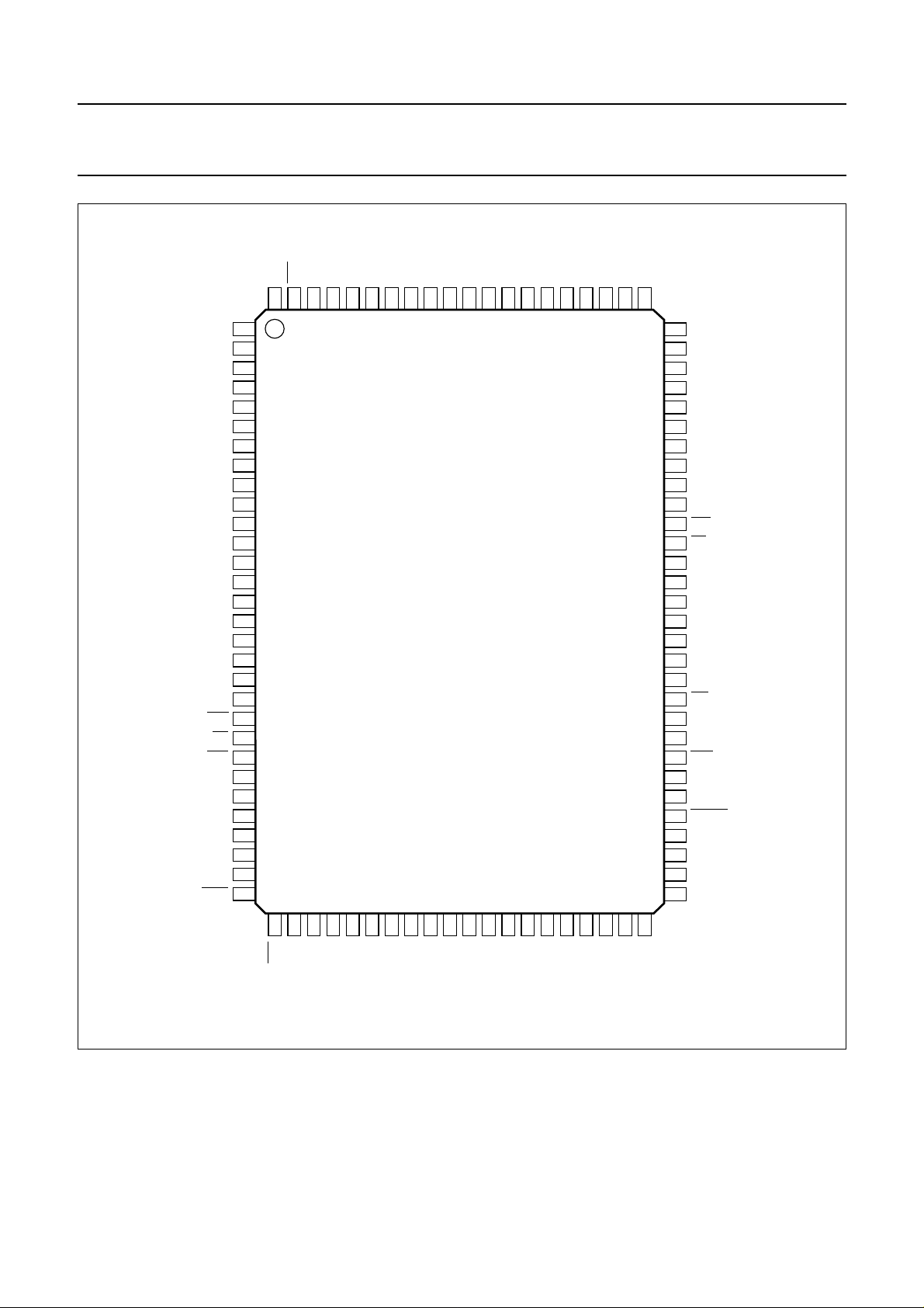
7 PINNING
SYMBOL PIN TYPE DESCRIPTION
ADC 1 input analog-to-digital converter DC input
AIF 2 input analog-to-digital converter IF input
V
SSA
ADE 99 input analog-to-digital converter enable (active LOW)
V
DDA
INP[0:9] 8 to 17 input 2048 kHz IF or baseband digital parallel input data (8 or 10 bits)
ADCLK 19 output analog-to-digital clock output 8192 kHz if
IQS 20 input clock signal indicating I or Q baseband data if
BYP 21 input IF input stage bypass (active LOW)
FSI 22 input frame sync input (LOW indicates DAB null symbol detection)
FSO 23 output null detector/frame sync output (LOW indicates DAB null symbol position)
SLI 24 output AGC synchronization lock indicator (HIGH if synchronized)
AGC 25 output AGC level comparator output (HIGH if input sample > reference level, else LOW)
OSCI 4 input oscillator or system clock input, 24576 kHz
OSCO 5 output oscillator output
MCLK 41 output master clock output, 24576 kHz
V
SS
V
DD
TEST 92 input connect to ground for proper operation
OUT[0:7] 32 to 39 output baseband or channel impulse response output
OCLK 27 output output data clock (negative edge indicates new data)
OIQ 29 output output I or Q select signal if
OCIR 30 input output select: baseband if OCIR = HIGH, CIR if OCIR = LOW
OEN 31 input output enable (active LOW)
CFIC 51 output microcontroller interface signal indicating Fast Information Channel (FIC) processing
CMODE 52 input microcontroller interface mode input (only L3-bus)
CDATA 53 I/O microcontroller interface serial data I
CCLK 54 input microcontroller interface clock input I
RESET 55 input chip reset input (active LOW)
A[17:11] 62 to 68 output address outputs external RAM
A[10:0] 81 to 91 output address outputs external RAM
WR 61 output write data to RAM (active LOW)
RD 69 output read data from RAM (active LOW)
A17 70 output address bit 17 inverted for second RAM (128k × 8)
D[0:7] 71 to 78 I/O data input/output external RAM
3 ground analog supply ground
100 supply analog voltage supply (+3.3 V)
signal for swapping I and Q data bytes if BYP = HIGH
7, 18,
supply digital supply ground
26, 40,
60, 80
and 94
6, 28,
supply digital voltage supply (+3.3 V)
42 and
79
BYP = HIGH, 4096 kHz if BYP = LOW
BYP = LOW;
OCIR = HIGH, or frame trigger if OCIR = LOW
2
C-bus or L3-bus (5 V tolerant)
2
C-bus or L3-bus
2000 Jun 14 5

Philips Semiconductors Preliminary specification
Digital audio broadcast channel decoder SAA3500H
SYMBOL PIN TYPE DESCRIPTION
SOV3 44 output serial output valid data 3
SOV2 45 output serial output valid data 2
SOV1 46 output serial output valid data 1
SOD3 47 output serial output data 3
SOD2 48 output serial output data 2
SOD1 49 output serial output data 1 (from channel decoder)
SOC 50 output serial output clock (384 kHz continuous)
REF 43 output receiver error flag [from Viterbi decoder, for Simple Full Capacity Output (SFCO)]
SFCO 56 output simple full capacity output (direct from Viterbi decoder)
RDC 57 output receiver data clock (6144 kHz continuous) or SFCO clock (burst)
RDE 58 input RDI output enable (active LOW)
RDO 59 output receiver data interface bi-phase output
TDO 93 output boundary scan test serial output
TCK 95 input boundary scan test clock input
TDI 96 input boundary scan test serial input
TMS 97 input boundary scan test mode select input
TRST 98 input boundary scan test reset input
2000 Jun 14 6
Philips Semiconductors Preliminary specification
Digital audio broadcast channel decoder SAA3500H
DDA
V
TRST
TMS
TDI
TCK
VSSTDO
ADC
AIF
V
SSA
OSCI
OSCO
V
DD
V
SS
INP0
INP1
INP2
INP3
INP4
INP5
INP6
INP7
INP8
INP9
V
SS
ADCLK
IQS
BYP
FSI
FSO
SLI
AGC
V
SS
OCLK
V
DD
OIQ
OCIR
ADE
99989796959493929190898887868584838281
100
1
2
3
4
5
6
7
8
9
10
11
12
13
14
15
16
17
18
19
20
21
22
23
24
25
26
27
28
29
TESTA0A1A2A3A4A5A6A7A8A9
SAA3500H
A10
80
79
78
77
76
75
74
73
72
71
70
69
68
67
66
65
64
63
62
61
60
59
58
57
56
55
54
53
52
5130
V
SS
V
DD
D0
D1
D2
D3
D4
D5
D6
D7
A17
RD
A11
A12
A13
A14
A15
A16
A17
WR
V
SS
RDO
RDE
RDC
SFCO
RESET
CCLK
CDATA
CMODE
CFIC
31323334353637383940414243444546474849
OEN
OUT0
OUT1
OUT2
OUT3
OUT4
OUT5
OUT6
OUT7
Fig.2 Pin configuration.
2000 Jun 14 7
50
MXXxxx
SS
DD
MCLK
REF
V
SOV3
SOV2
SOV1
SOD3
SOD2
SOD1
SOC
V

Philips Semiconductors Preliminary specification
Digital audio broadcast channel decoder SAA3500H
8 FUNCTIONAL DESCRIPTION
The 2.048 MHz IF signal is digitized by an 8-bit flash
Analog-to-Digital Converter (ADC), which samples at
8.192 MHz. The required input level is limited to a
peak-to-peak voltage of 2 V. Due to a fast
sample-and-hold circuit sub-sampling is possible, so that
all IF frequencies of N × 8.192 ±2.048 MHz can be used.
If a higher resolution ADC is wanted, anexternal ADCcan
be connected.
The digital mixer accepts a 2.048 MHzIF signal atits input
and converts it to baseband with In-phase (I) and
Quadrature-phase (Q) components. The mixer frequency
is adjusted on a DAB frame basis with 1 Hz resolution to
prevent performance degradation. The mixer output
signals are digitally filtered and subjected to internal
Automatic Gain Control (AGC) before entering the
subsequent Fast Fourier Transform (FFT) stage.
The output of the digital AGC detectors indicates for each
input sample whether the level is below or above the
reference input level. By means of external filtering and
gain control, the signal can be used to adjust the input
signal level of the analog-to-digital converter (external
AGC).
The on-chip null detector operates on the digital baseband
signal and indicates the coarse position of the DAB null
symbol (FSO = LOW), which is used for time base
initialization. The spacing of detected null symbols is used
to detect the DAB transmission mode.
The time base counts samples on a symbol and a frame
basis in order to generate the internal control windows for
the FFT and to generate a frame sync signal (FSO) during
thenullsymbol.Initializationofthe time base is determined
by the null detector signal (FSI) and the selected DAB
mode. After time base initialization the SAA3500H will be
in symbol processing mode and the null detector will be
deactivated.
The OFDM symbol demodulator applies a real-time FFT
and differential demodulation to the baseband signal. The
output is quantized to 4-bit metrics for the Viterbi decoder.
The position of the FFT window is adjusted on a DAB
frame basis in order to avoid Inter-Symbol Interference
(ISI).
TheFFTresultof the reference symbol is processed bythe
synchronization core, which performs two functions:
estimation of the frequency error of the baseband signal,
which is needed to adjust the digital mixer (AFC), and
calculation of the Channel Impulse Response (CIR) to be
used for positioning of the FFT window and the system
clock.All timing and frequency controlloopsare realized in
the synchronization core and can be influenced from the
control interface.
The Viterbi decoder is preceded by frequency and time
de-interleavingof the incoming metricsinexternal RAM, to
distribute burst errors caused by channel fading. Variable
rate decoding is done with 3.072 Mb/s decision speed.
Output bits are re-encoded and compared to
corresponding input bits in order to generate an error flag
signal.
Sub-channel selection is done on a Capacity Unit (CU)
basis. All standardized Unequal Error Protection (UEP)
puncturing schemes for audio and Equal Error Protection
(EEP) schemes for data are provided. Up to
64 sub-channelscanbeselectedseparately,whichmeans
virtually unlimited DAB decoding capabilities.
The output interface provides a full-speed standardized
Receiver Data Interface (RDI) for all sub-channel data.
This allows to extend every DAB receiver with external
decoders for all kind of services. A dedicated interface is
provided for the Philips SAA2502H audio source decoder,
which completes the DAB receiver.
The system clock of 24.576 MHz, can be generated by an
integrated DCXO, which is internally locked to the DAB
signal. The clockis available on the MCLKpin to provide a
synchronous clock to the MPEG decoder and
microcontroller.
The I2C-bus or L3-bus configurable control interface
provides access to Automatic Frequency Control (AFC),
Channel Impulse Response (CIR), Fast Information
Channel (FIC) and sub-channel selection controls.
2000 Jun 14 8

Philips Semiconductors Preliminary specification
Digital audio broadcast channel decoder SAA3500H
9 INTERFACE DESCRIPTION
9.1 Input interface
The input interface can be used in 3 different modes, depending on the bypass (BYP) and IQ Select (IQS) pins. Digital
input data should be in two’s complement format (optionally: offset binary) and synchronized with the ADCLK output
signal. Input data are read on the rising edge of ADCLK.
Table 1 Input modes
BYP IQS DESCRIPTION
0 clk digital baseband input sampled at 2048 kHz and with I and Q data multiplexed
1 0 digital IF input sampled at 8192 kHz, internal I/Q demodulator
1 1 digital IF input sampled at 8192 kHz, internal I/Q demodulator with I and Q swapped
In case of baseband input the IQ select signal shall indicate whether the current sample is either I or Q data (INP[9:0]).
ADCLK
INP[9:0]
IQS
Q
I
0
1
Q
I
1
Q
2
2
4096 kHz
10 bits
2048 kHz
Fig.3 Baseband input signals (BYP = LOW).
Digital IF input is, typically, at a frequency of 2048 kHz. It is possible to apply sub-sampling on a N × 8.192 ±2.048 MHz
(N = 1, 2, 3,...,19) IF signal, but care should be taken with the jitter of the crystal clock, which is proportional to N.
ADCLK
INP[9:0]
8192 kHz
10 bits
Fig.4 IF input signals [BYP = HIGH, IQS = LOW (no swap) or HIGH (swap)].
To use the on-chip null detector, pins
FSI and FSO shall simply be connected to each other.
When using an external null detector, the FSI input shall indicate the position of the null symbol in the baseband signal
(FSI = LOW). The negative edge may have a maximum delay of 512 samples with respect to an ideal null detector. The
delay compensation can be set via the I2C/L3 interface (register ATCWinControl). The FSI input provides edge jitter
suppression of up to 40 samples starting from the first negative edge. Once the SAA3500H is in symbol processing
mode, the FSI signal is ignored. During the null detection state, the Sync Lock Indicator (SLI) will be continuously LOW.
9.2 Memory interface
An external SRAM memory of either 128 or 256 kbytes is required to store the metrics from the data de-interleaver for
half (432 CUs) or full (864 CUs) decoding capacity, respectively. The upper address line A17 is available both true and
inverted (A17) to allow memory extension without an address decoder. 3.3 V RAMs should be used with either an 8 or
(2 ×) 4-bit data bus and an access time of ≤80 ns. Input data are read on the rising edge of RD, output data shall be
latched on the rising edge of WR.
2000 Jun 14 9

Philips Semiconductors Preliminary specification
Digital audio broadcast channel decoder SAA3500H
A[17:0]
D[7:0]
RD
WR
Fig.5 RAM access.
9.3 Parallel output interface
The digital parallel output interface can be used in 3 different modes depending on the OCIR and OEN select pins.
Output data shall be latched on the falling edge of OCLK.
Table 2 Parallel output modes
X = don’t care.
OCIR OEN DESCRIPTION
0 0 channel impulse response sampled at 64 kHz, OIQ = frame trigger
1 0 baseband sampled at 2048 kHz and with I and Q data multiplexed
X 1 OUT[7:0], OIQ and OCLK disabled
By means of an external digital-to-analog converter, either the CIR or I/Q data can be displayed on an oscilloscope.
Digitaloutput data isclockedout on thefallingedge of theOCLKoutput signal. Incaseof baseband outputtheOIQ signal
indicates, if the current sample is either I or Q data.
OCLK
OUT[7:0]
OIQ
QIQIQ
4096 kHz
signed
2048 kHz
Fig.6 Baseband output signals (OCIR = HIGH, OEN = LOW).
OCLK
OUT[7:0]
OIQ
64 kHz
unsigned
trigger
Fig.7 CIR output signals (OCIR = LOW, OEN = LOW).
2000 Jun 14 10

Philips Semiconductors Preliminary specification
Digital audio broadcast channel decoder SAA3500H
In the CIR output mode the channel impulse response is clocked out in a burst of N (unsigned) samples at 64 kHz each
frame after CIR processing (bit SyncBusy = logic 0). The edges of the frame trigger signal (OIQ) allow to trigger a CIR
display either at the start of the symbol or at the start of the symbol guard. In the latter case the CIR peak for a Gaussian
channel will be at the left of the display.
9.4 Serial output interface
The serial output interface is intended for transferring up to three sub-channels to the source decoder(s) with a total
maximum bit rate of 384 kbit/s. The sub-channels for these outputs should be selected with the appropriate I2C or L3
commands. The output clock is 384 kHz. Each sub-channel has its own serial data and data valid line, but the clock is
common. Serial output data shall be latched on the rising edge of SOC.
SOC
SOD
SOV
Fig.8 DAB3 serial output.
9.5 Simple full capacity output
This interface provides serial access to all the Viterbi decoder output bits without any formatting. Transmission framing
is indicated by the CFIC window, which can also be used to separate the FIC data (CFIC = HIGH) from the Main Service
Channel (MSC) data (CFIC = LOW). The bit CFICMode can be used to signal on CFIC the beginning of the selected
sub-channels (CFICMode = logic 0). The clock is a 3072 kHz burst clock, activated for each new output bit.
Accompanied with the data is the error flag, obtained by re-encoding the Viterbi output bits and comparison with the
corresponding Viterbi decoder input bits (REF = HIGH for error bit).
CFIC
RDC
SFCO
REF
CFICMode = 0
Fig.9 Simple full capacity output (CFICMode = logic 1).
9.6 RDI output
For external use a bi-phase modulated output (RDO) is provided, which carries all the FIC and MSC data, formatted
according to the DAB receiver data interface specification
“EN 50255”
, which is based on the IEC 60958 digital audio
interface. Optionally, a clock (6144 kHz) and word select signal (48 kHz) can be provided (instead of SFCO signals).
Transmitter Identification Information (TII) is not signalled on this RDI. The FIC however is always signalled, with the
Cyclic Redundancy Check (CRC) performed and the Error Check Field containing the resulting CRC (normally 0).
Selected sub-channels will be directed to the RDI interface in the extended capacity mode (22 bits for MSC), but the
number of RDI frames and the reliability are not signalled (i.e., set to all logic 0s and all logic 1s, respectively).
2000 Jun 14 11

Philips Semiconductors Preliminary specification
Digital audio broadcast channel decoder SAA3500H
RDO
Fig.10 RDI output (normal mode, RDE = LOW).
In case SFCO data output is not desired, a particular ‘RDI plus’ mode can be selected, which provides a continuous
6144 kHz clock on RDC, synchronous to the bi-phase RDI data and accompanied by a fixed word select signal, to allow
RDI source reception without an extra clock recovery circuit. Output data shall be latched on the rising edge of RDC.
RDC
RDO
SFCO
Channel 1 (32 bits)
Channel 2 (32 bits)
Fig.11 RDI output (RDI plus mode, RDE = LOW).
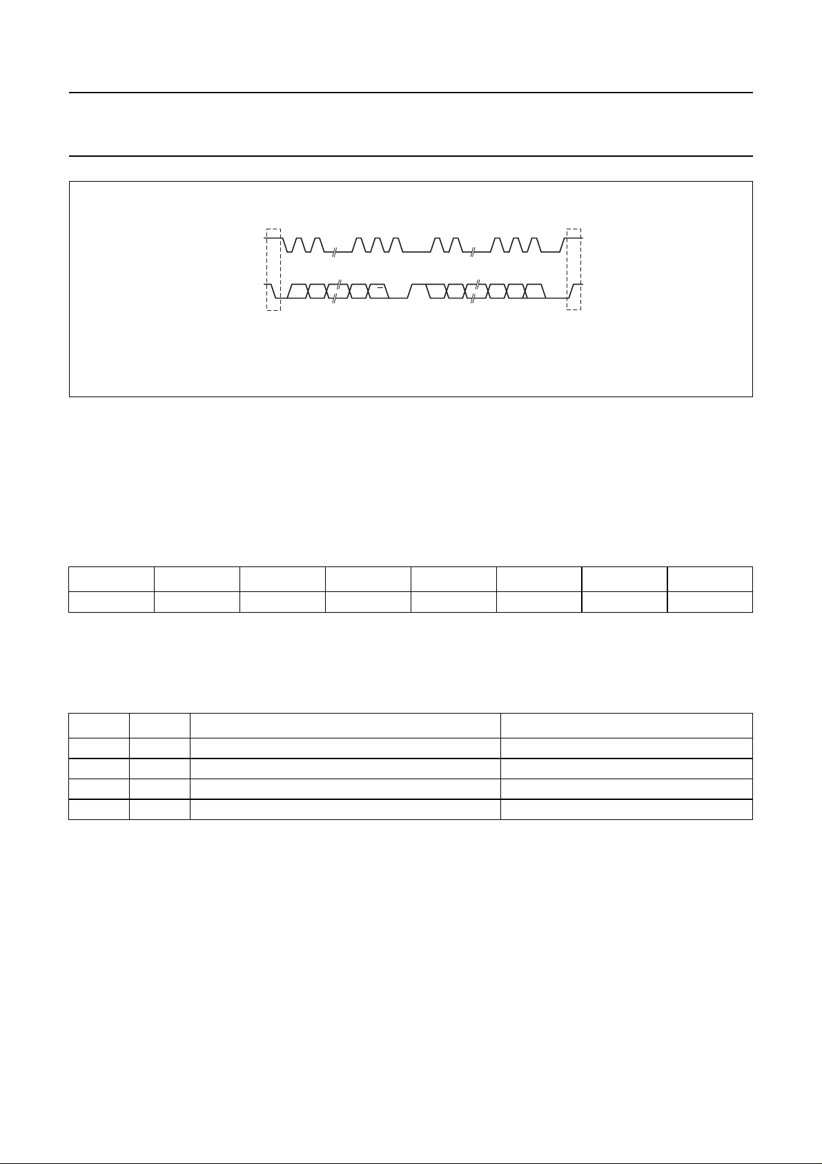
9.7 Microcontroller interface
The microcontroller interface of the SAA3500H operates in one of two distinct modes of operation: I2C-bus or L3-bus.
Mode setting is determined at initialization, as described in Fig.12. On either control bus data are transferred in 8-bit
packets, or bytes.
The interface uses three signals and the function in the L3-bus mode or I2C-bus mode is indicated in Table 3.
Table 3 Control bus modes
SIGNAL L3-BUS MODE I2C-BUS MODE DIRECTION DESCRIPTION
CDATA L3DATA SDA input/output microcontroller interface serial data
CCLK L3CLK SCL input microcontroller interface bit clock
CMODE L3MODE none input microcontroller interface mode select
During a hard reset of the device, the microcontroller interface mode is determined. As a consequence, the interface
cannot be used while the reset signal is asserted. Mandatory action must be taken for correct microcontroller interface
start-up at a hard reset, as explained in Fig.12.
RESET
CMODE
CCLK
phase 1 phase 2 phase 3
I2C-bus mode
L3-bus mode
Fig.12 Microcontroller interface initialization procedure.
2000 Jun 14 12

Philips Semiconductors Preliminary specification
Digital audio broadcast channel decoder SAA3500H
In phase 1, the level of the CMODE signal determines the microcontroller interface mode, while reset is asserted.
CMODE = HIGHdefines I2C-busmode, CMODE = LOW definesL3-bus mode. No transferscan be performed, asCCLK
must be HIGH.
Inphase 2, which isfor L3-bus modeof operation only, it is mandatory totake CMODE HIGH,then LOW againafter reset
hasbeen de-asserted, tocorrectly initialize the interface unit. This mustoccur before anyL3-bus transfer (even toor from
other devices) is performed. CCLK shall remain HIGH during this phase.
In phase 3, the first transfer can be performed on the microcontroller interface.
Any deviation from these steps may result in undefined behaviour of the microcontroller interface, even with the
possibility of disturbing transfers to other devices connected to the control bus.
At a hardware reset, all writeable data items are forced to their default values.
The microcontroller interface provides access to all blocks, which generate or need control information. Selections on
the SAA3500H are at the sub-channel level, the required sub-channel parameters should be obtained via the Multiplex
Configuration Information (MCI), which is part of the FIC.
The CFIC window from the SAA3500H indicates FIC decoding. FIC data from the I2C/L3 interface will be invalid, if
CFIC = HIGH. It is therefore recommended to connect CFIC to a microcontroller interrupt input pin. With regard to the
real-time processing requirements, it is highly recommended to use a 16-bit microcontroller.
2
9.7.1 I
C-BUS MODE
The implemented I2C-bus interface isof the 400 kbit/s, 7-bit address type. TheCDATA output driver is of the ‘opendrain’
type in order to be compliant with the I2C-bus specification. The device address is as follows:
Table 4 I
2
C-bus device address
BIT 7 BIT 6 BIT 5 BIT 4 BIT 3 BIT 2 BIT 1 BIT 0
1101011R/
Bit 7to bit 1 comprise the7-bit I
2
C-busslave address, while bit 0indicates the transfer directionof data and acknowledge
W
bits as follows:
2
Table 5 Read and write operation to the microcontroller in I
W FUNCTION REMARK
R/
C-bus mode
0 data from microcontroller to SAA3500H all acknowledge generated by SAA3500H
1 data from SAA3500H to microcontroller acknowledge for data generated by microcontroller
Fundamentals of the I2C-bus interface protocol are shown in Fig.13.
2000 Jun 14 13
Philips Semiconductors Preliminary specification
Digital audio broadcast channel decoder SAA3500H
CCLK
CDATA
S
START
condition
2
1
address transfer data transfer
MSB
78
R/W
ACK
9
27
MSB LSB
9
81
ACK
P
STOP
condition
Fig.13 I2C-bus data transfer example.
For full details of the I2C-bus interface specification, please, refer to the I2C-bus specification
(http://www.semiconductors.com/handbook/various_38.html), which is also available on request.
9.7.2 L3-BUS MODE
The L3-bus device address is composed as follows:
Table 6 L3-bus device address
BIT 7 BIT 6 BIT 5 BIT 4 BIT 3 BIT 2 BIT 1 BIT 0
011011DOM1
(1)
DOM0
(1)
Note
1. The ‘Data Operation Mode’ bits DOM1 and DOM0 define the current sub-mode of the microcontroller interface until
the next time a device address is received (see Table 7).
Table 7 Read and write operation to the microcontroller in L3-bus mode
DOM1 DOM0 FUNCTION REMARK
0 0 data from microcontroller to SAA3500H general purpose data transfer
0 1 data from SAA3500H to microcontroller general purpose data transfer
1 0 control from microcontroller to SAA3500H register selection for data transfer
1 1 status from SAA3500H to microcontroller short device status message
Fundamentals of the L3-bus interface protocol are shown in Fig.14.
2000 Jun 14 14

Philips Semiconductors Preliminary specification
Digital audio broadcast channel decoder SAA3500H
CCLK
CMODE
CDATA
1
addressing mode
2
78
MSBLSB
27
1
data mode
8
MSBLSB
Fig.14 L3-bus command transfer example.
For full details of the L3-bus interface specification, please, refer to the SAA2502H data sheet (order number
9397 750 03068 or at http://www.semiconductors.com/products).
9.7.3 MICROCONTROLLER INTERFACE REGISTERS
Communication between the microcontroller and the SAA3500H is by addressing registers and writing or reading data.
All addresses and register contents are in hexadecimal notation.
The following registers are available for the writing of data:
Table 8 Writeable registers
ADDRESS
(HEX)
NAME DESCRIPTION
SETTING AFTER RESET
(HEX)
00 Control control 1F
01 Configuration configuration FF
10 CIFCount CIF count and occurrence change flag 00 00 00
20 CurSubChSel current sub-channel selection 00 00 00 00
21 NextSubChSel next sub-channel selection 00 00 00 00
30 SOD1 select sub-channel for serial output SOD1 40
31 SOD2 select sub-channel for serial output SOD2 40
32 SOD3 select sub-channel for serial output SOD3 40
40 AGCExternal setting of thresholds for external AGC 61 0C
41 AGCInternal settings of the internal AGC D0 49
42 AGCFixed internal AGC switch off and fixed gain setting 00
50 NullDetMargin null detector margin 40
51 TIIControl TII main/sub identifier 00 00
60 MixerFreqInput digital mixer frequency control input 80 00 00
62 CarrierShift carrier shift by n carrier positions 00
63 AFCGain AFC loop gain 10
70 ATCWinControl ATC window control input or FFT window position and null
96
detector delay compensation
71 CIRThreshold CIR detector thresholds, edge and range 02 02
73 ATCGains ATC loops gains; clock I and P gains and window gain 02 04 20
2000 Jun 14 15

Philips Semiconductors Preliminary specification
Digital audio broadcast channel decoder SAA3500H
The following registers are available for the reading of data:
Table 9 Readable registers
ADDRESS
(HEX)
NAME DESCRIPTION BYTES TO READ
00 Status internal processing status 1
10 FICErrCount FIC error count per frame 2
20 to 2B FICData FIC data inclusive CRC result 32
51 TIIOutput TII complex phase values 6
60 AFCLoopOutput AFC loop output for digital mixer frequency control 3
61 CarrierDev AFC carrier deviation detector 2
70 ATCWinOutput ATC window loop output for FFT window position 1
71 ATCDetector ATC CIR detector output 3
72 ATCClockOutput ATC clock loop output for external VCXO 1
76 CIRPower power of CIR response 2
A description of how to use the individual registers is given in a separate application note.
10 LIMITING VALUES
In accordance with the Absolute Maximum Rating System (IEC 60134).
SYMBOL PARAMETER CONDITIONS MIN. MAX. UNIT
V
DD
V
i
I
DD
I
i
I
o
P
tot
T
stg
T
amb
V
es
DC supply voltage note 1 −0.5 +6 V
input voltage −0.5 VDD+ 0.5 V
supply current − 200 mA
input current −10 +10 mA
output current −10 +10 mA
total power dissipation − 650 mW
storage temperature −65 +150 °C
operating ambient temperature −40 +85 °C
electrostatic handling voltage note 2 −300 +300 V
note 3 −3000 +3000 V
Notes
1. All supply connections must be made to the same external power supply unit.
2. Machine model: equivalent to discharging a 200 pF capacitor through a 0 Ω series resistor (‘0 Ω’ is actually
0.75 µH+10Ω).
3. Human body model: equivalent to discharging a 100 pF capacitor through a 1500 Ω series resistor.
11 THERMAL CHARACTERISTICS
SYMBOL PARAMETER CONDITIONS VALUE UNIT
R
th(j-a)
thermal resistance from junction to ambient in free air 60 K/W
2000 Jun 14 16

Philips Semiconductors Preliminary specification
Digital audio broadcast channel decoder SAA3500H
12 DC CHARACTERISTICS
VDD= 3.0 to 3.6 V; T
SYMBOL PARAMETER CONDITIONS MIN. TYP. MAX. UNIT
Supplies
V
DD(tot)
I
DD(tot)
total DC supply voltage note 1 3.0 3.3 3.6 V
total DC supply current −−180 mA
Dissipation
P
tot
total power dissipation −−650 mW
Inputs
= −40 to +85 °C; all voltages referenced to ground (VSS); unless otherwise specified.
amb
CMOS
V
V
|I
C
LEVEL INPUT (INP[9:0], FSI, CCLK AND TCK)
IH
IL
| input leakage current VI= 0 or VI=VDD−−1µA
LI
i
HIGH-level input voltage 2.0 −−V
LOW-level input voltage −−0.8 V
input capacitance − 5 − pF
CMOS LEVEL INPUT, PULL-UP (BYP, CMODE, IQS, OCIR, OEN, RDE, TDI, TMS AND TRST)
V
IH
V
IL
R
pu(VDD)(int)
C
i
HIGH-level input voltage 2.0 −−V
LOW-level input voltage −−0.8 V
internal pull-up resistor to V
DD
16 33 78 kΩ
input capacitance − 5 − pF
CMOS LEVEL INPUT, HYSTERESIS, PULL-UP (RESET)
V
IH(hys)
V
IL(hys)
V
hys
R
pu(VDD)(int)
C
i
HIGH-level hysteresis input, rising edge 1.4 − 1.9 V
LOW-level hysteresis input, falling edge 0.9 − 1.45 V
hysteresis voltage 0.4 − 0.7 V
internal pull-up resistor to V
DD
16 33 78 kΩ
input capacitance − 5 − pF
Inputs/outputs
CMOS LEVEL INPUT, HYSTERESIS, OPEN DRAIN OUTPUT (CDATA)
V
IH(hys)
V
IL(hys)
V
hys
V
OL
CMOS LEVEL INPUT, OUTPUT STAGE (D[7:0])
V
IH
V
IL
| input leakage current VI= 0 or VI=VDD−−1µA
|I
LI
V
OH
V
OL
HIGH-level hysteresis input, rising edge 1.4 − 1.9 V
LOW-level hysteresis input, falling edge 0.9 − 1.45 V
hysteresis voltage 0.4 − 0.7 V
LOW-level output voltage I
=3mA −−0.4 V
LOAD
1.5 mA
HIGH-level input voltage 2.0 −−V
LOW-level input voltage −−0.8 V
HIGH-level output voltage I
LOW-level output voltage I
= −1.5 mA 2.4 −−V
LOAD
= 1.5 mA −−0.4 V
LOAD
2000 Jun 14 17

Philips Semiconductors Preliminary specification
Digital audio broadcast channel decoder SAA3500H
SYMBOL PARAMETER CONDITIONS MIN. TYP. MAX. UNIT
Outputs
CMOS LEVEL, OUTPUT STAGE (A[17:0], A17, ADCLK, AGC, FSO, OCLK, OIQ, RD, SLI, SOD[1:3], SOV[1:3]
AND WR)
V
OH
V
OL
C
LOAD
CMOS LEVEL,3-STATE OUTPUT STAGE, (OUT[7:0])
V
OH
V
OL
|I
| output leakage current inactive mode;
LO
1.5 mA
HIGH-level output voltage I
LOW-level output voltage I
= −1.5 mA 2.4 −−V
LOAD
= 1.5 mA −−0.4 V
LOAD
output load capacitance −−30 pF
1.5 mA
HIGH-level output voltage I
LOW-level output voltage I
= −1.5 mA 2.4 −−V
LOAD
= 1.5 mA −−0.4 V
LOAD
−−1µA
VO= 0 or
VO=V
DD
C
LOAD
CMOS LEVEL, OUTPUT STAGE (CFIC, MCLK, RDC, RDO, REF, SFCO, SOC AND TDO)
V
OH
V
OL
C
LOAD
output load capacitance −−30 pF
3 mA
HIGH-level output voltage I
LOW-level output voltage I
= −3 mA 2.4 −−V
LOAD
=3mA −−0.4 V
LOAD
output load capacitance −−50 pF
Note
1. All supply connections must be made to the same external power supply unit.
13 AC CHARACTERISTICS
VDD= 3.0 to 3.6 V; T
=25°C; all voltages referenced to ground (VSS); unless otherwise specified.
amb
SYMBOL PARAMETER CONDITIONS MIN. TYP. MAX. UNIT
Oscillator input (OSC)
f
i(OSC)
δ
OSC
input frequency note 1 − 24576 − kHz
input clock duty factor 40 − 60 %
Reset input (RESET)
t
CL,RESET
reset LOW duration note 2 60 × T −−ns
Input interface (ADCLK, BYP, INP[9:0] and IQS)
BASEBAND INPUT (BYP = LOW); see Fig.15
T
cy,ADCLK
t
CL,ADCLK
t
CH,ADCLK
t
h,INP
t
h,IQS
ADCLK cycle time − 244 − ns
ADCLK LOW time − 122 − ns
ADCLK HIGH time − 122 − ns
INP[9:0] hold time 5 −−ns
IQS hold time −−80 ns
2000 Jun 14 18

Philips Semiconductors Preliminary specification
Digital audio broadcast channel decoder SAA3500H
SYMBOL PARAMETER CONDITIONS MIN. TYP. MAX. UNIT
IF INPUT (BYP = HIGH); see Fig.16
T
cy,ADCLK
t
CL,ADCLK
t
CH,ADCLK
t
h,INP
t
d,INP
Memory interface (A17, A[17:0], D[7:0], RD and WR); see Figs 17 and 18
T
cy,A
t
CL,RD
t
d,RD
t
h,RD
t
CL,WR
t
d,WR
t
d,D
t
h,D
Parallel output interface (OCIR, OCLK, OEN, OIQ and OUT[9:0])
ADCLK cycle time − 122 − ns
ADCLK LOW time − 80 − ns
ADCLK HIGH time − 42 − ns
INP[9:0] hold time 5 −−ns
INP[9:0] delay time −−25 ns
address cycle time − 326 − ns
RD LOW time − 163 − ns
RD delay time − 40 − ns
RD hold time − 0 − ns
WR LOW time − 163 − ns
WR delay time 0 40 − ns
data delay time − 0 − ns
data hold time −−5ns
BASEBAND OUTPUT (OCIR = HIGH); see Fig.19
T
cy,OCLK
t
CL,OCLK
t
CH,OCLK
t
su,OUT
t
su,OIQ
OCLK cycle time − 244 − ns
OCLK LOW time − 122 − ns
OCLK HIGH time − 122 − ns
OUT[7:0] set-up time − 15 − ns
OIQ set-up time − 17 − ns
CIR OUTPUT (OCIR = LOW); see Fig.20
T
cy,OCLK
t
CL,OCLK
t
CH,OCLK
t
su,OUT
t
su,OIQ
OCLK cycle time − 15.6 −µs
OCLK LOW time − 8.3 −µs
OCLK HIGH time − 7.3 −µs
OUT[7:0] set-up time − 0 − ns
OIQ set-up time − 0 − ns
Serial output interface (SOC, SOD[3:1] and SOV[3:1]); see Fig.21
T
cy,SOC
t
CL,SOC
t
CH,SOC
t
h,SOD
t
su,SOV
t
h,SOV
SOC cycle time − 2.6 −µs
SOC LOW time − 1.3 −µs
SOC HIGH time − 1.3 −µs
SOD hold time − 0 − ns
SOV set-up time − 4 − ns
SOV hold time − 2 − ns
2000 Jun 14 19

Philips Semiconductors Preliminary specification
Digital audio broadcast channel decoder SAA3500H
SYMBOL PARAMETER CONDITIONS MIN. TYP. MAX. UNIT
Simple full capacity output interface (CFIC, RDC, REF and SFCO); see Fig.22
t
CH,CFIC
t
SH,CFIC
t
su,CFIC
t
h,CFIC
T
cy,RDC
t
CH,RDC
t
CL,RDC
t
su,SFCO
t
su,REF
t
h,REF
RDI output interface (RDC, RDE, RDO and SFCO)
CFIC HIGH time DAB mode I − 3.738 − ms
DAB mode II − 0.935 − ms
DAB mode III − 1.246 − ms
DAB mode IV − 1.869 − ms
CFIC strobe HIGH time bit CFICMode = 0 − 75 − ns
bit CFICMode = 1 − 0 − ns
CFIC set-up time − 165 − ns
CFIC hold time − 80 − ns
RDC cycle time 325 −−ns
RDC HIGH time 250 −−ns
RDC LOW time − 75 − ns
SFCO set-up time − 5 − ns
REF set-up time − 165 − ns
REF hold time −−160 − ns
NORMAL MODE; see Fig.23
t
ONE
t
ZERO
ONE time − 163 − ns
ZERO time − 326 − ns
RDI PLUS MODE; see Fig.24
T
cy,RDC
t
CH,RDC
t
CL,RDC
T
cy,SFCO
t
CH,SFCO
t
CL,SFCO
t
su,SFCO
t
h,SFCO
RDC cycle time − 163 − ns
RDC HIGH time − 86 − ns
RDC LOW time − 77 − ns
SFCO cycle time − 20.8 −µs
SFCO HIGH time − 10.4 −µs
SFCO LOW time − 10.4 −µs
SFCO set-up time − 4 − ns
SFCO hold time − 0 − ns
Microcontroller interface
INITIALIZATION PROCEDURE; see Fig.25
t
CL,RESET
t
d,RES-MOD
t
CH,CMODE
t
d,MOD-CLK
RESET LOW time note 2 60 × T −−ns
delay time from RESET to CMODE note 2 10 × T −−ns
CMODE HIGH time note 2 10 × T −−ns
delay time from CMODE to first CCLK note 2 10× T −−ns
2000 Jun 14 20

Philips Semiconductors Preliminary specification
Digital audio broadcast channel decoder SAA3500H
SYMBOL PARAMETER CONDITIONS MIN. TYP. MAX. UNIT
L3-BUS MICROCONTROLLER TO SLAVE DEVICE; see Figs 26 and 28
t
cL
t
cH
t
d1
t
h1
t
h2
t
su
t
L
L3-BUS SLAVE DEVICE TO MICROCONTROLLER; see Fig.27
t
d2
t
d3
t
d4
t
d5
t
h3
I2C-BUS INPUTS/OUTPUT (CDATA AND CCLK)
t
f,I2C
f
CCLK
Notes
1. In a real application, the clock frequency may vary in a range of ±50 ppm due to timing synchronization.
2. T=4×OSC cycle time, i.e., T = 163 ns at f
L3CLK LOW time note 2 T + 10 −−ns
L3CLK HIGH time note 2 T + 10 −−ns
L3MODE set-up time before first L3CLK
10 −−ns
LOW
L3DATA hold time after L3CLK HIGH 10 −−ns
L3MODE hold time after last L3CLK HIGH 15 −−ns
L3DATA set-up time before L3CLK HIGH note 2 T + 10 −−ns
L3MODE LOW time note 2 T + 10 −−ns
L3MODE HIGH to L3DATA enabled time 0 − 20 ns
L3MODE HIGH to L3DATA stable time −−20 ns
L3CLK HIGH to L3DATA stable time note 2 −−2T + 30 ns
L3MODE LOW to L3DATA disabled time 0 − 20 ns
L3DATA hold time after L3CLK HIGH note 2 T −−ns
output fall time −−250 ns
CCLK clock frequency −−400 kHz
= 24.576 MHz.
osc
T
cy,ADCLK
ADCLK
INP[9:0]
t
h,INP
IQS
Fig.15 Baseband input timing (BYP = LOW).
T
cy,ADCLK
ADCLK
INP[9:0]
t
h,INP
Fig.16 IF input timing [BYP = HIGH, IQS = LOW (no swap) or HIGH (swap)].
2000 Jun 14 21
t
CL,ADCLK
t
CL,ADCLK
t
CH,ADCLK
t
h,IQS
t
CH,ADCLK
t
d,INP

Philips Semiconductors Preliminary specification
Digital audio broadcast channel decoder SAA3500H
T
cy,A
t
h,D
t
CL,WR
A[17:0]
D[7:0]
RD
T
cy,A
A[17:0]
D[7:0]
t
t
CL,RD
t
t
d,RD
h,D
WR
d,D
t
d,WR
Fig.17 RAM access read timing.
T
cy,OCLK
t
CH,OCLK
t
OCLK
CL,OCLK
OUT[7:0]
t
t
su,OUT
su,OIQ
OIQ
Fig.19 Baseband output timing (OCIR = HIGH,
OEN = LOW).
Fig.18 RAM access write timing.
T
cy,OCLK
t
CH,OCLK
t
OCLK
CL,OCLK
OUT[7:0]
t
su,OIQ
t
su,OUT
OIQ
Fig.20 CIR output timing (OCIR = LOW,
OEN = LOW).
T
SOC
t
cy,SOC
CL,SOC
t
CH,SOC
t
h,SOD
SOD
SOV
t
su,SOV
t
h,SOV
Fig.21 DAB3 serial output timing.
2000 Jun 14 22

Philips Semiconductors Preliminary specification
Digital audio broadcast channel decoder SAA3500H
t
t
su,CFIC
CFIC
RDC
SFCO
t
su,SFCO
REF
Fig.22 Simple full capacity output timing.
CH,CFIC
T
cy,RDC
t
CH,RDC
t
su,REF
t
h,CFIC
t
CL,RDC
t
h,REF
t
SH,CFIC
t
ONE
t
ZERO
RDO
Fig.23 RDI output timing (normal mode, RDE = LOW).
T
cy,RDC
t
CL,RDC
t
CH,RDC
RDC
RDO
t
h,SFCO
t
CL,SFCO
t
su,SFCO
SFCO
t
T
cy,SFCO
CH,SFCO
Fig.24 RDI output timing (RDI plus mode, RDE = LOW).
2000 Jun 14 23

Philips Semiconductors Preliminary specification
Digital audio broadcast channel decoder SAA3500H
t
CL,RESET
t
CH,CMODE
handbook, full pagewidth
L3MODE
L3CLK
L3DATA
RESET
CMODE
CCLK
t
d,RES-MOD
t
d,MOD-CLK
Fig.25 Microcontroller interface initialization timing.
t
d1 h2
t
cL
t
cH
t
h1
t
su
Fig.26 Timing of L3-bus addressing mode.
t
MGB507
t
handbook, full pagewidth
d1 h2
L3MODE
t
cL
t
cH
L3CLK
t
su
t
L3DATA
microcontroller
to IC
L3DATA
IC to
microcontroller
t
d2
t
d3
h1
t
h3
t
d4
Fig.27 Timing of L3-bus data transfer mode.
2000 Jun 14 24
t
t
d5
MGB508

Philips Semiconductors Preliminary specification
Digital audio broadcast channel decoder SAA3500H
t
handbook, full pagewidth
L3MODE
t
h2
L3CLK
t
L3DATA
IC to
microcontroller
d5
Fig.28 Timing of L3-bus halt mode.
14 APPLICATION INFORMATION
A suggestion for an application block diagram is shown in Fig.29.
L
t
d1
t
d2
MGB509
TUNER
BAND III/L
SAW
FILTER
AGC
MICROCONTROLLER
Fig.29 Typical application diagram.
14.1 Clock oscillator
To perform automatic fine tuning of the clock signal, the
microcontroller reads data from the SAA3500H and
controls an external (VCXO) crystal oscillator. The
following requirements should be met by that oscillator:
Table 10 VCXO specification
PARAMETER VALUE UNIT
Frequency 24576 kHz
Pull range ±50 ppm
Operating temperature −40 to +85 °C
Frequency drift with temperature ≤±20 ppm
Tolerance and ageing ≤±10 ppm
RAM
(256k × 8)
A
SAA3500H
24.576 MHz
D
DAB3
I2C or L3-BUS
SAA2502H
RDI
I2S
L/R
SPDIF
14.2 Reset input
The reset signal is active LOW and should have a
minimum duration of 60 clock cycles.
14.3 Boundary scan test interface
For normal operation set TRST LOW, TCK LOW or HIGH,
TDI and TMS not connected or HIGH. The boundary scan
chain has a length of 84 and a 5-bit instruction code.
2000 Jun 14 25
Philips Semiconductors Preliminary specification
Digital audio broadcast channel decoder SAA3500H
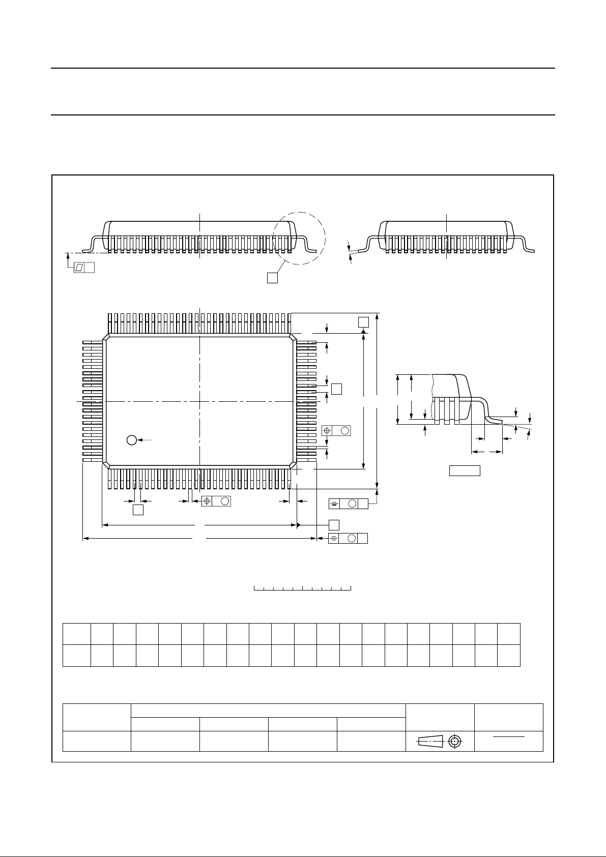
15 PACKAGE OUTLINE
QFP100: plastic quad flat package;
100 leads (lead length 1.95 mm); body 14 x 20 x 2.7 mm; high stand-off height
c
y
X
SOT317-1
80 51
81
pin 1 index
100
1
b
0.25
p
D
H
D
cE
p
0.40
0.25
0.25
0.13
e
DIMENSIONS (mm are the original dimensions)
mm
A
max.
3.3
0.36
0.10
2.87
2.57
UNIT A1A2A3b
A
50
Z
E
e
H
E
w M
b
p
31
30
w M
D
20.1
19.9
Z
D
0 5 10 mm
scale
(1)
(1) (1)(1)
eH
H
D
14.1
13.9
0.65
24.2
23.6
B
E
18.2
17.6
v M
A
v M
B
LL
1.0
0.6
p
A
2
A
E
0.151.95 0.10.2
(A )
A
1
L
detail X
Zywv θ
Z
E
D
0.8
1.0
0.4
0.6
3
θ
L
p
o
7
o
0
Note
1. Plastic or metal protrusions of 0.25 mm maximum per side are not included.
OUTLINE
VERSION
SOT317-1 MO-112
IEC JEDEC EIAJ
REFERENCES
2000 Jun 14 26
EUROPEAN
PROJECTION
ISSUE DATE
97-08-01
99-12-27

Philips Semiconductors Preliminary specification
Digital audio broadcast channel decoder SAA3500H
16 SOLDERING
16.1 Introduction to soldering surface mount
packages
Thistextgives a very brief insighttoacomplex technology.
A more in-depth account of soldering ICs can be found in
our
“Data Handbook IC26; Integrated Circuit Packages”
(document order number 9398 652 90011).
There is no soldering method that is ideal for all surface
mount IC packages. Wave soldering is not always suitable
for surface mount ICs, or for printed-circuit boards with
high population densities. In these situations reflow
soldering is often used.
16.2 Reflow soldering
Reflow soldering requires solder paste (a suspension of
fine solder particles, flux and binding agent) to be applied
tothe printed-circuit board byscreenprinting, stencilling or
pressure-syringe dispensing before package placement.
Several methods exist for reflowing; for example,
infrared/convection heating in a conveyor type oven.
Throughput times (preheating,soldering and cooling) vary
between 100 and 200 seconds depending on heating
method.
Typical reflow peak temperatures range from
215 to 250 °C. The top-surface temperature of the
packages should preferable be kept below 230 °C.
16.3 Wave soldering
Conventional single wave soldering is not recommended
forsurfacemount devices (SMDs) or printed-circuit boards
with a high component density, as solder bridging and
non-wetting can present major problems.
To overcome these problems the double-wave soldering
method was specifically developed.
• Use a double-wave soldering method comprising a
turbulent wave with high upward pressure followed by a
smooth laminar wave.
• For packages with leads on two sides and a pitch (e):
– larger than or equal to 1.27 mm, the footprint
longitudinal axis is preferred to be parallel to the
transport direction of the printed-circuit board;
– smaller than 1.27 mm, the footprint longitudinal axis
must be parallel to the transport direction of the
printed-circuit board.
The footprint must incorporate solder thieves at the
downstream end.
• Forpackageswith leads on four sides, thefootprint must
be placed at a 45° angle to the transport direction of the
printed-circuit board. The footprint must incorporate
solder thieves downstream and at the side corners.
During placement andbefore soldering, the package must
be fixed with a droplet of adhesive. The adhesive can be
applied by screen printing, pin transfer or syringe
dispensing. The package can be soldered after the
adhesive is cured.
Typical dwell time is 4 seconds at 250 °C.
A mildly-activated flux will eliminate the need for removal
of corrosive residues in most applications.
16.4 Manual soldering
Fix the component by first soldering two
diagonally-opposite end leads. Use a low voltage (24 V or
less) soldering iron applied to the flat part of the lead.
Contact time must be limited to 10 seconds at up to
300 °C.
When using a dedicated tool, all other leads can be
soldered in one operation within 2 to 5 seconds between
270 and 320 °C.
If wave soldering is used the following conditions must be
observed for optimal results:
2000 Jun 14 27

Philips Semiconductors Preliminary specification
Digital audio broadcast channel decoder SAA3500H
16.5 Suitability of surface mount IC packages for wave and reflow soldering methods
PACKAGE
WAVE REFLOW
(1)
BGA, SQFP not suitable suitable
SOLDERING METHOD
HLQFP, HSQFP, HSOP, HTSSOP, SMS not suitable
(3)
PLCC
, SO, SOJ suitable suitable
LQFP, QFP, TQFP not recommended
SSOP, TSSOP, VSO not recommended
(2)
(3)(4)
(5)
suitable
suitable
suitable
Notes
1. All surface mount (SMD) packages are moisture sensitive. Depending upon the moisture content, the maximum
temperature (with respect to time) and body size of the package, there is a risk that internal or external package
cracks may occur due to vaporization of the moisture in them (the so called popcorn effect). For details, refer to the
Drypack information in the
“Data Handbook IC26; Integrated Circuit Packages; Section: Packing Methods”
.
2. These packages are not suitable for wave soldering as a solder joint between the printed-circuit board and heatsink
(at bottom version) can not be achieved, and as solder may stick to the heatsink (on top version).
3. If wave soldering is considered, then the package must be placed at a 45° angle to the solder wave direction.
The package footprint must incorporate solder thieves downstream and at the side corners.
4. Wave soldering is only suitable for LQFP, TQFP and QFP packages with a pitch (e) equal to or larger than 0.8 mm;
it is definitely not suitable for packages with a pitch (e) equal to or smaller than 0.65 mm.
5. Wave soldering is only suitable for SSOP and TSSOP packages with a pitch (e) equal to or larger than 0.65 mm; it is
definitely not suitable for packages with a pitch (e) equal to or smaller than 0.5 mm.
2000 Jun 14 28

Philips Semiconductors Preliminary specification
Digital audio broadcast channel decoder SAA3500H
17 DATA SHEET STATUS
DATA SHEET STATUS
PRODUCT
STATUS
DEFINITIONS
(1)
Objective specification Development This data sheet contains the design target or goal specifications for
product development. Specification may change in any manner without
notice.
Preliminary specification Qualification This data sheet contains preliminary data, and supplementary data will be
published at a later date. Philips Semiconductors reserves the right to
make changes at any time without notice in order to improve design and
supply the best possible product.
Product specification Production This data sheet contains final specifications. Philips Semiconductors
reserves the right to make changes at any time without notice in order to
improve design and supply the best possible product.
Note
1. Please consult the most recently issued data sheet before initiating or completing a design.
18 DEFINITIONS
Short-form specification The data in a short-form
specification is extracted from a full data sheet with the
same type number and title. For detailed information see
the relevant data sheet or data handbook.
Limiting values definition Limiting values given are in
accordance with the Absolute Maximum Rating System
(IEC 60134). Stress above one or more of the limiting
values may cause permanent damage to the device.
These are stress ratings only and operation of the device
atthese or at any otherconditionsabovethose given in the
Characteristics sections of the specification is not implied.
Exposure to limiting values for extended periods may
affect device reliability.
Application information Applications that are
described herein for any of these products are for
illustrative purposes only. Philips Semiconductors make
norepresentationorwarranty that such applications will be
suitable for the specified use without further testing or
modification.
19 DISCLAIMERS Life support applications These products are not
designed for use in life support appliances, devices, or
systems where malfunction of these products can
reasonably be expected to result in personal injury. Philips
Semiconductorscustomersusingorselling these products
for use in such applications do so at their own risk and
agree to fully indemnify Philips Semiconductors for any
damages resulting from such application.
Right to make changes Philips Semiconductors
reserves the right to make changes, without notice, in the
products, including circuits, standard cells, and/or
software, described or contained herein in order to
improve design and/or performance. Philips
Semiconductors assumes no responsibility or liability for
theuseof any of these products, conveysnolicenceortitle
under any patent, copyright, or mask work right to these
products,and makes no representations orwarrantiesthat
these products are free from patent, copyright, or mask
work right infringement, unless otherwise specified.
2
20 PURCHASE OF PHILIPS I
Purchase of Philips I
C COMPONENTS
2
C components conveys a license under the Philips’ I2C patent to use the
components in the I2C system provided the system conforms to the I2C specification defined by
Philips. This specification can be ordered using the code 9398 393 40011.
2000 Jun 14 29

Philips Semiconductors Preliminary specification
Digital audio broadcast channel decoder SAA3500H
NOTES
2000 Jun 14 30

Philips Semiconductors Preliminary specification
Digital audio broadcast channel decoder SAA3500H
NOTES
2000 Jun 14 31

Philips Semiconductors – a w orldwide compan y
Argentina: see South America
Australia: 3 Figtree Drive, HOMEBUSH, NSW 2140,
Tel. +61 2 9704 8141, Fax. +61 2 9704 8139
Austria: Computerstr. 6, A-1101 WIEN, P.O. Box 213,
Tel. +43 1 60 101 1248, Fax. +43 1 60 101 1210
Belarus: Hotel Minsk Business Center, Bld. 3, r. 1211, Volodarski Str. 6,
220050 MINSK, Tel. +375 172 20 0733, Fax. +375 172 20 0773
Belgium: see The Netherlands
Brazil: see South America
Bulgaria: Philips Bulgaria Ltd., Energoproject, 15th floor,
51 James Bourchier Blvd., 1407 SOFIA,
Tel. +359 2 68 9211, Fax. +359 2 68 9102
Canada: PHILIPS SEMICONDUCTORS/COMPONENTS,
Tel. +1 800 234 7381, Fax. +1 800 943 0087
China/Hong Kong: 501 Hong Kong Industrial Technology Centre,
72 Tat Chee Avenue, Kowloon Tong, HONG KONG,
Tel. +852 2319 7888, Fax. +852 2319 7700
Colombia: see South America
Czech Republic: see Austria
Denmark: Sydhavnsgade 23, 1780 COPENHAGEN V,
Tel. +45 33 29 3333, Fax. +45 33 29 3905
Finland: Sinikalliontie 3, FIN-02630 ESPOO,
Tel. +358 9 615 800, Fax. +358 9 6158 0920
France: 51 Rue Carnot, BP317, 92156 SURESNES Cedex,
Tel. +33 1 4099 6161, Fax. +33 1 4099 6427
Germany: Hammerbrookstraße 69, D-20097 HAMBURG,
Tel. +49 40 2353 60, Fax. +49 40 2353 6300
Hungary: see Austria
India: Philips INDIA Ltd, Band Box Building, 2nd floor,
254-D, Dr. Annie Besant Road, Worli, MUMBAI 400 025,
Tel. +91 22 493 8541, Fax. +91 22 493 0966
Indonesia: PT Philips DevelopmentCorporation, Semiconductors Division,
Gedung Philips, Jl. Buncit Raya Kav.99-100, JAKARTA 12510,
Tel. +62 21 794 0040 ext. 2501, Fax. +62 21 794 0080
Ireland: Newstead, Clonskeagh, DUBLIN 14,
Tel. +353 1 7640 000, Fax. +353 1 7640 200
Israel: RAPAC Electronics, 7 Kehilat Saloniki St, PO Box 18053,
TEL AVIV 61180, Tel. +972 3 645 0444, Fax. +972 3 649 1007
Italy: PHILIPS SEMICONDUCTORS, Via Casati, 23 - 20052 MONZA (MI),
Tel. +39 039 203 6838, Fax +39 039 203 6800
Japan: Philips Bldg 13-37, Kohnan 2-chome, Minato-ku,
TOKYO 108-8507, Tel. +81 3 3740 5130, Fax. +81 3 3740 5057
Korea: Philips House, 260-199 Itaewon-dong, Yongsan-ku, SEOUL,
Tel. +82 2 709 1412, Fax. +82 2 709 1415
Malaysia: No. 76 Jalan Universiti, 46200 PETALING JAYA, SELANGOR,
Tel. +60 3 750 5214, Fax. +60 3 757 4880
Mexico: 5900 Gateway East, Suite 200, EL PASO, TEXAS 79905,
Tel. +9-5 800 234 7381, Fax +9-5 800 943 0087
Middle East: see Italy
Netherlands: Postbus 90050, 5600 PB EINDHOVEN, Bldg. VB,
Tel. +31 40 27 82785, Fax. +31 40 27 88399
New Zealand: 2 Wagener Place, C.P.O. Box 1041, AUCKLAND,
Tel. +64 9 849 4160, Fax. +64 9 849 7811
Norway: Box 1, Manglerud 0612, OSLO,
Tel. +47 22 74 8000, Fax. +47 22 74 8341
Pakistan: see Singapore
Philippines: Philips Semiconductors Philippines Inc.,
106 Valero St. Salcedo Village, P.O. Box 2108 MCC, MAKATI,
Metro MANILA, Tel. +63 2 816 6380, Fax. +63 2 817 3474
Poland: Al.Jerozolimskie 195 B, 02-222 WARSAW,
Tel. +48 22 5710 000, Fax. +48 22 5710 001
Portugal: see Spain
Romania: see Italy
Russia: Philips Russia, Ul. Usatcheva 35A, 119048 MOSCOW,
Tel. +7 095 755 6918, Fax. +7 095 755 6919
Singapore: Lorong 1, Toa Payoh, SINGAPORE 319762,
Tel. +65 350 2538, Fax. +65 251 6500
Slovakia: see Austria
Slovenia: see Italy
South Africa: S.A. PHILIPS Pty Ltd., 195-215 Main Road Martindale,
2092 JOHANNESBURG, P.O. Box 58088 Newville 2114,
Tel. +27 11 471 5401, Fax. +27 11 471 5398
South America: Al. Vicente Pinzon, 173, 6th floor,
04547-130 SÃO PAULO, SP, Brazil,
Tel. +55 11 821 2333, Fax. +55 11 821 2382
Spain: Balmes 22, 08007 BARCELONA,
Tel. +34 93 301 6312, Fax. +34 93 301 4107
Sweden: Kottbygatan 7, Akalla, S-16485 STOCKHOLM,
Tel. +46 8 5985 2000, Fax. +46 8 5985 2745
Switzerland: Allmendstrasse 140, CH-8027 ZÜRICH,
Tel. +41 1 488 2741 Fax. +41 1 488 3263
Taiwan: Philips Semiconductors, 6F, No. 96, Chien Kuo N. Rd., Sec. 1,
TAIPEI, Taiwan Tel. +886 2 2134 2886, Fax. +886 2 2134 2874
Thailand: PHILIPS ELECTRONICS (THAILAND) Ltd.,
209/2 Sanpavuth-Bangna Road Prakanong, BANGKOK 10260,
Tel. +66 2 745 4090, Fax. +66 2 398 0793
Turkey: Yukari Dudullu, Org. San. Blg., 2.Cad. Nr. 28 81260 Umraniye,
ISTANBUL, Tel. +90 216 522 1500, Fax. +90 216 522 1813
Ukraine: PHILIPS UKRAINE, 4 Patrice Lumumba str., Building B, Floor 7,
252042 KIEV, Tel. +380 44 264 2776, Fax. +380 44 268 0461
United Kingdom: Philips Semiconductors Ltd., 276 Bath Road, Hayes,
MIDDLESEX UB3 5BX, Tel. +44 208 730 5000, Fax. +44 208 754 8421
United States: 811 East Arques Avenue, SUNNYVALE, CA 94088-3409,
Tel. +1 800 234 7381, Fax. +1 800 943 0087
Uruguay: see South America
Vietnam: see Singapore
Yugoslavia: PHILIPS, Trg N. Pasica 5/v, 11000 BEOGRAD,
Tel. +381 11 3341 299, Fax.+381 11 3342 553
For all other countries apply to: Philips Semiconductors,
International Marketing & Sales Communications, Building BE-p, P.O. Box 218,
5600 MD EINDHOVEN, The Netherlands, Fax. +31 40 27 24825
© Philips Electronics N.V. SCA
All rights are reserved. Reproduction in whole or in part is prohibited without the prior written consent of the copyright owner.
The information presented in this document does not form part of any quotation or contract, is believed to be accurate and reliable and may be changed
without notice. No liability will be accepted by the publisher for any consequence of its use. Publication thereof does not convey nor imply any license
under patent- or other industrial or intellectual property rights.
2000
Internet: http://www.semiconductors.philips.com
69
Printed in The Netherlands 753503/01/pp32 Date of release: 2000 Jun 14 Document order number: 9397 750 07187
 Loading...