

Philips SAA3010P-S285, SAA3010T-S285, SAA3010U-N2 Datasheet

DATA SH EET
Product specification
File under Integrated Circuits, IC01
June 1989
INTEGRATED CIRCUITS
SAA3010
Infrared remote control transmitter
RC-5

June 1989 2
Philips Semiconductors Product specification
Infrared remote control transmitter RC-5 SAA3010
FEATURES
• Low voltage requirement
• Biphase transmission technique
• Single pin oscillator
• Test mode facility
GENERAL DESCRIPTION
The SAA3010 is intended as a general purpose (RC-5)
infrared remote control system for use where a low voltage
supply and a large debounce time are expected.
The device can generate 2048 different commands and
utilizes a keyboard with a single pole switch for each key.
The commands are arranged so that 32 systems can be
addressed, each system containing 64 different
commands. The keyboard interconnection is illustrated by
Fig.3.
The circuit response to legal (one key pressed at a time)
and illegal (more than one key pressed at a time) keyboard
operation is specified in the section “Keyboard operation”.
QUICK REFERENCE DATA
Note
1. V
DD
+0.5 V must not exceed 9 V.
PACKAGE OUTLINES
28-lead DIL plastic; (SOT117); SOT117-1; 1996 September 11.
28-lead mini-pack; plastic (SO28; SOT136A); SOT136-1; 1996 September 11.
PARAMETER SYMBOL MIN. TYP. MAX. UNIT
Supply voltage range V
DD
2 − 7V
Input voltage range (note 1) V
I
−0.5 − VDD+0.5 V
Input current I
I
−−±10 mA
Output voltage range (note 1) V
O
−0.5 − VDD+0.5 V
Output current I
O
−−±10 mA
Operating ambient temperature
range
T
amb
−25 − 85 °C
WARNING
The use of this device must conform with the Philips Standard number URT-0421.
June 1989 3
Philips Semiconductors Product specification
Infrared remote control transmitter RC-5 SAA3010
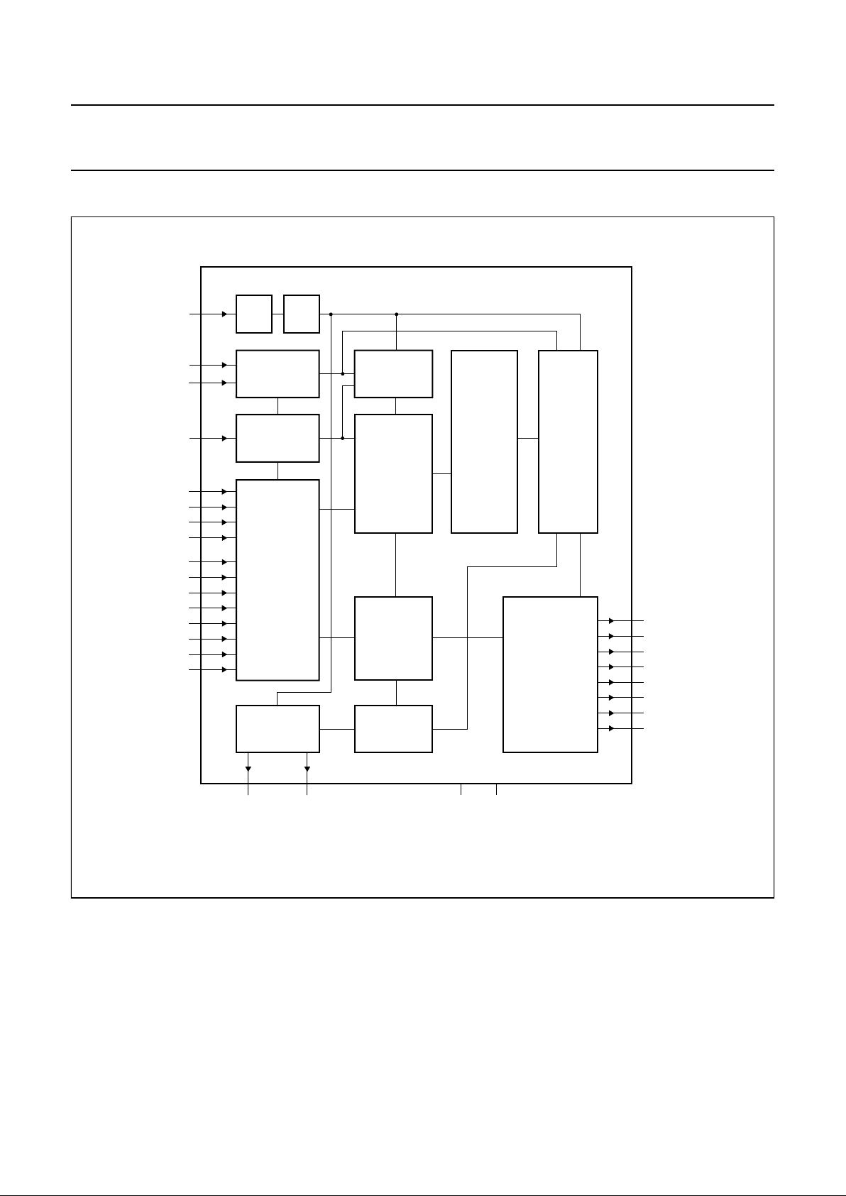
BLOCK DIAGRAM
handbook, full pagewidth
MGE347
KEYBOARD
ENCODER
MODE
SELECTION
TEST
MODE
OSC
3 × 2
1
OUTPUT
COMMAND
AND
SYSTEM
ADDRESS
LATCH
PARALLEL
TO SERIAL
CONVERTER
MASTER
RESET
GENERATOR
CONTROL
UNIT
DECODER
2
13
DIVIDER
KEYBOARD
DRIVER
DECODER
18
20
19
2
6
5
4
3
1
27
26
25
24
23
22
21
8
7
17
16
15
13
12
11
10
9
14
28
SAA3010
OSC
TP1
TP2
SSM
Z3
Z2
Z1
Z0
X7
X6
X5
X4
X3
X2
X1
X0
DATA
MDATA
VSSV
DD
DR0
DR1
DR2
DR3
DR4
DR5
DR6
DR7
Fig.1 Block diagram.
June 1989 4
Philips Semiconductors Product specification
Infrared remote control transmitter RC-5 SAA3010
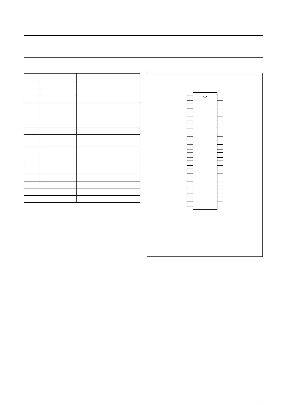
PINNING
Note
1. (I) = input
(IPU) = input with p-channel pull-up transistor
(ODN) = output with open drain n-channel transistor
(OP3) = output 3-state
PIN MNEMONIC
(1)
FUNCTION
1 X7 (IPU) sense input from key matrix
2 SSM (I) system mode selection input
3-6 Z0-Z3 (IPU) sense inputs from key matrix
7 MDATA (OP3) generated output data
modulated with 1/12 the
oscillator frequency at a 25%
duty factor
8 DATA (OP3) generated output information
9-13 DR7-DR3
(ODN)
scan drivers
14 V
SS
ground (0 V)
15-17 DR2-DR0
(ODN)
scan drivers
18 OSC (I) oscillator input
19 TP2 (I) test point 2
20 TP1 (I) test point 1
21-27 X0-X6 (IPU) sense inputs from key matrix
28 V
DD
(I) voltage supply
handbook, halfpage
X7
SSM
Z0
Z1
Z2
Z3
MDATA
DATA
DR7
DR6
DR5
DR4
DR3
V
SS
V
DD
X6
X5
X4
X2
X1
X3
X0
TP1
TP2
OSC
DR0
DR1
DR2
1
2
3
4
5
6
7
8
9
10
11
12
13
28
27
26
25
24
23
22
21
20
19
18
17
16
1514
SAA3010
MGE346
Fig.2 Pinning diagram.
June 1989 5
Philips Semiconductors Product specification
Infrared remote control transmitter RC-5 SAA3010
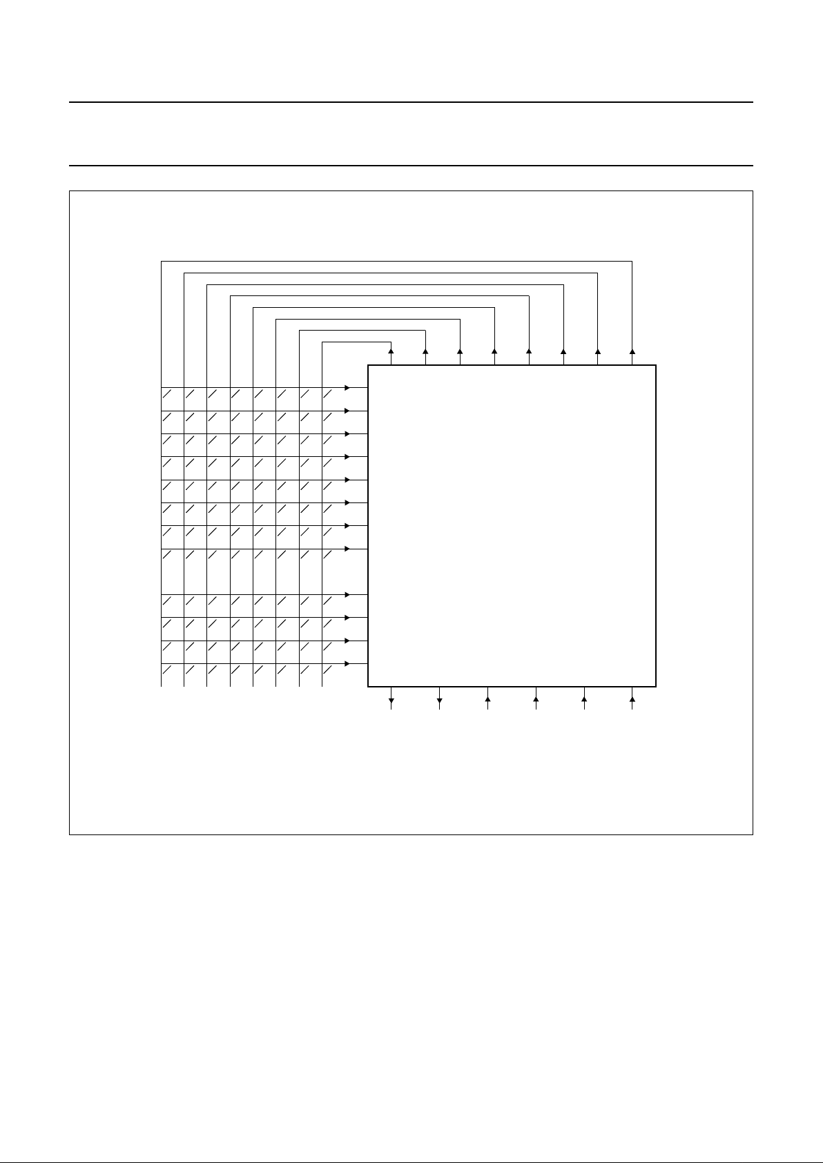
Fig.3 Keyboard interconnection.
handbook, full pagewidth
Z0
Z1
Z2
Z3
X0
X1
X2
X3
X4
X5
X6
X7
DR0 DR1 DR2 DR3 DR4 DR5 DR6 DR7
DATA MDATA SSM TP1 TP2 OSC
MGE348
17 16 15 13 12 11 10 9
21
22
23
24
25
26
27
1
3
4
5
6
8 7 2 20 19 18
SAA3010

June 1989 6
Philips Semiconductors Product specification
Infrared remote control transmitter RC-5 SAA3010
FUNCTIONAL DESCRIPTION
Keyboard operation
Every connection of one X-input and one DR-output will be recognized as a legal key operation and will cause the device
to generate the corresponding code. The same applies to every connection of one Z-input to one DR-output with the
proviso that SSM must be LOW. When SSM is HIGH a wired connection must exist between a Z-input and a DR-output.
If no connection is present the system number will not be generated. Activating two or more X-inputs, Z-inputs or Z-inputs
and X-inputs at the same time is an illegal action and inhibits further activity (oscillator will not start).
When one X- or Z-input is connected to more than one DR-output, the last scan signal will be considered as legal.
The maximum value of the contact series resistance of the switched keyboard is 7 kΩ.
Inputs
In the quiescent state the command inputs X0 to X7 are held HIGH by an internal pull-up transistor. When the system
mode selection (SSM) input is LOW and the system is quiescent, the system inputs Z0 to Z3 are also held HIGH by an
internal pull-up transistor. When SSM is HIGH the pull-up transistor for the Z-inputs is switched off, in order to prevent
current flow, and a wired connection in the Z-DR matrix provides the system number.
Outputs
The output signal DATA transmits the generated information in accordance with the format illustrated by Fig.4 and
Tables 1 and 2. The code is transmitted using a biphase technique as illustrated by Fig.5. The code consists of four parts:
• Start part −1.5 bits (2 × logic 1)
• Control part −1 bit
• System part −5 bits
• Command part −6 bits
The output signal MDATA transmits the generated information modulated by 1/12 of the oscillator frequency with a 50%
duty factor.
In the quiescent state both DATA and MDATA are non-conducting (3-state outputs).
The scan driver outputs DR0 to DR7 are open drain n-channel transistors and conduct when the circuit is quiescent.
After a legal key operation the scanning cycle is started and the outputs switched to the conductive state one by one.
The DR-outputs were switched off at the end of the preceding debounce cycle.
 Loading...