

Philips SAA2521GP Datasheet

INTEGRATED CIRCUITS
DATA SH EET
SAA2521
Masking threshold processor for
MPEG layer 1 audio compression
applications
Preliminary specification
File under Integrated Circuits, IC01
August 1993

Philips Semiconductors Preliminary specification
Masking threshold processor for MPEG
SAA2521
layer 1 audio compression applications
FEATURES
• Stereo or 2-channel mono encoding
• Status may be read continuously
• Microcontroller interface
• I2S-interfaces
• Allocation algorithm including optional emphasis
correction (for 44.1 kHz)
• Reduced power consumption
• 4 V nominal operating voltage capability.
ORDERING INFORMATION
EXTENDED TYPE
NUMBER
SAA2521GP 44 QFP plastic SOT205AG
Note
1. SOT205-1; 1996 August 23.
PINS PIN POSITION MATERIAL CODE
GENERAL DESCRIPTION
The SAA2521 performs the adaptive allocation and
scaling function for calculating the masking thresholds and
sub-band sample accuracy in MPEG layer 1 applications.
The SAA2521 is intended for use in conjunction with the
stereo filter codec SAA2520.
PACKAGE
(1)
August 1993 2

Philips Semiconductors Preliminary specification
Masking threshold processor for MPEG
layer 1 audio compression applications
handbook, full pagewidth
SWS
FS256
FDAF
NODONE
RESOL0
RESOL1
FDIR
FRESET
FSYNC
SCALE
TEST3
TEST4
31
39
34
INTERFACE INTERFACECOMPENSATION DELAY
20
21
22
37
36
35
38
15
16
CONTROL
SAA2521
ALLOCATION AND
SCALING
CALCULATION
V
DD
14,24,40
SAA2521
33
FDAC
32
SCL
LTDATA
LTCNT1
LTCNT0
LTENA
LTCLK
CLK24
RESET
PWRDWN
5
1
2
3
4
26
23
30
LT INTERFACE
6,25,44
V
SS
11
7
8
9
10
MLB137
LTDATAC
LTCNT1C
LTCNT0C
LTENC
LTCLKC
Fig.1 Block diagram.
August 1993 3

Philips Semiconductors Preliminary specification
Masking threshold processor for MPEG
layer 1 audio compression applications
SS
V
n.c.
n.c.
handbook, full pagewidth
LTCNT1
LTCNT0
LTENA
LTCLK
LTDATA
V
SS
LTCNT1C
LTCNT0C
LTENC
LTCLKC
LTDATAC
44
1
2
3
4
5
6
7
8
9
10
11
n.c.
43
42
41
SAA2521
SAA2521
DD
V
40
FS256
39
SCALE
38
FDIR
37
FRESET
FSYNC
36
35
FDAF
34
33
32
31
30
29
28
27
26
25
24
23
FDAC
SCL
SWS
PWRDWN
TEST10
TEST9
TEST8
CLK24
V
SS
V
DD
RESET
handbook, full pagewidth
AUDIO
SOURCE
MICROCONTROLLER
AMPLIFIER
ADC/DAC
AUDIO
digital audio interface
system micro interface
12
13
14
15
16
17
DD
V
TEST1
TEST2
TEST3
TEST4
TEST5
Fig.2 Pin configuration.
control
power down
reset
18
19
TEST6
TEST7
SAA2520
and
SAA2521
21
20
RESOL0
NODONE
22
MLB136
RESOL1
MPEG interface
MPEG
source/
receiver
MLB138
Fig.3 MPEG codec system data flow diagram.
August 1993 4

Philips Semiconductors Preliminary specification
Masking threshold processor for MPEG
SAA2521
layer 1 audio compression applications
PINNING
SYMBOL PIN DESCRIPTION TYPE
LTCNT1 1 mode control 1, microcontroller interface input I
LTCNT0 2 mode control 0, microcontroller interface input I
LTENA 3 enable microcontroller interface input I
LTCLK 4 bit clock microcontroller interface input I
LTDATA 5 data, microcontroller interface (3-state inputs/outputs) I/O
V
SS
LTCNT1C 7 control 1; microcomputer interface O
LTCNT0C 8 control 0; microcomputer interface O
LTENC 9 enable microcontroller interface O
LTCLKC 10 bit clock; microcontroller interface O
LTDATAC 11 data; microcontroller interface, (3-state inputs/outputs) I/O
TEST1 12 test output; do not connect
TEST2 13 test output; do not connect
V
DD
TEST3 15 test mode input; to be connected to V
TEST4 16 test mode input; to be connected to V
TEST5 17 test input; to be connected to V
TEST6 18 test input; to be connected to V
TEST7 19 test input; to be connected to V
NODONE 20 no done state selection input I
RESOL0 21 resolution selection 0 input I
RESOL1 22 resolution selection 1 input I
RESET 23 active HIGH reset input I
V
DD
V
SS
CLK24 26 24.576 MHz processing clock input I
TEST8 27 test input; to be connected to V
TEST9 28 test input; to be connected to V
TEST10 29 test input; to be connected to V
PWRDWN 30 power-down input I
SWS 31 word selection input; (Filtered) - I
SCL 32 bit clock input; (Filtered) - I
FDAC 33 filtered data (Filtered) - I
FDAF 34 filtered data (Filtered) - I
FSYNC 35 sub-band synchronization on (Filtered) - I
FRESET 36 reset signal input from SAA2520 I
FDIR 37 direction of the I
SCALE 38 scale factor index select (note 1) I
FS256 39 system clock input; sample frequency × 256 I
V
DD
6 supply ground (0 V)
14 positive supply voltage (+ 5 V)
24 positive supply voltage (+ 5 V)
25 supply ground (0 V)
2
S-interface I
2
S-interface (3-state inputs/outputs) I/O
2
S-interface (3-state inputs/outputs) I/O
2
S-interface; input I
40 positive supply voltage (+ 5 V)
DD
DD
SS
SS
SS
SS
SS
SS
2
S-interface I
2
S-interface, input I
August 1993 5

Philips Semiconductors Preliminary specification
Masking threshold processor for MPEG
SAA2521
layer 1 audio compression applications
SYMBOL PIN DESCRIPTION TYPE
n.c. 41 not connected
n.c. 42 not connected
n.c. 43 not connected
V
SS
Note to the Pinning Description
1. The scale input must be set LOW for use with the SAA2521.
FUNCTIONAL DESCRIPTION
Coding System
This efficient MPEG audio encoder is used in conjunction
with the SAA2520 filter codec (bit rates of 384, 256, 192
and 128 k bits/s). The encoder utilizes a system producing
sub-band samples from an incoming digital audio signal.
This relies upon the audibility of signals above a given
level and upon high amplitude signals masking those of
lower amplitude. Although each sub-band signal is of
approximately 750 Hz bandwidth, it possesses
considerable overlap with those adjacent to it.
During the process of encoding, the masking threshold
processor analyses the broadband audio signal at
sampling frequency f
signals at a sampling frequency (fs/32).
The coded signal consists of frames conveying the
information corresponding to the sub-band samples.
These also include a synchronization pattern identifying
the start of each new frame. The allocation information for
the 32 sub-bands is transferred as 4-bit values. If the
amplitude of a sub-band signal is below the masking
threshold it will be omitted from the coded signal.
The duration of a MPEG frame depends upon sampling
frequency and is adjusted to 384 divided by fs.
44 supply ground (0 V)
by splitting it into 32 sub-band
s
Encoding Mode
Signal FDIR sets the data flow direction on the
Filtered-I
the device will accept samples from FDAF. These will be
delayed by a number of sample periods depending upon
the setting of the SCALE input. In the instance of operation
with the SAA2520 (SCALE = logic 0) this delay will be 480
SWS periods. This will ensure alignment of the data with
the computed allocations.
After the delay the samples will be presented on FDAC
(pin 33). The circuit also performs all the calculations
required to build the allocation table which is used in the
codec (SAA2520). When used with the SAA2520 the
calculated scale factor indices are sent via the LT
interface. These operations are performed for every frame
of the sub-band codec.
In order to synchronize with the codec and utilize the
correct tables for the calculations the SAA2521 frequently
requests the status of the codec. It monitors the bit-rate,
sample frequency, operation mode and the emphasis
information and uses the 'ready to receive' bit of the codec
to determine the moment of the transfer of allocation
information.
Decoding Mode
2
S-interface. In the encoding mode (FDIR LOW)
Adaptive Allocation and Scaling
The coding system calculates the masking power of the
sub-band signals and adds the masking threshold.
Sub-band signals with power below this threshold denote
information to be discarded. Non-masked signals are
coded using floating point notation in which a mantissa
corresponds in length to the difference between peak
power and masking threshold. The process is repeated for
every MPEG frame and is known as the Adaptive
Allocation of the available capacity.
August 1993 6
In the decoding mode (FDIR HIGH) the SAA2521 will take
samples from FDAC which will be presented on the FDAF
after a delay of 160 SWS periods. The LT interface
between microcontroller and codec (SAA2520) will only be
affected by the 'ready to receive' bit from the codec
(SAA2520).

Philips Semiconductors Preliminary specification
Masking threshold processor for MPEG
layer 1 audio compression applications
Microcontroller Interface Operation
Information on the interface between microcontroller and
codec (SAA2520) will flow in a regular sequence
synchronized with the codec (SAA2520):
- with every FSYNC the SAA2521 will read the status of
the codec (SAA2520)
- Following the calculation of the allocation and scale
factors the SAA2521 will send the first allocation
information unit (16-bits). It will then continuously read
the codec (SAA2520) status to ascertain when it is
able to receive further allocation information units.
When the transfer of these units is complete the
SAA2521 will send settings and (for SCALE = logic 0)
scale factor indices.
- The extended settings will be sent to the codec as
soon as possible after reception from the
microcontroller.
The microcontroller communicates with the SAA2521 in
a similar fashion:
- status can be read continuously. The SAA2521 will
output a copy of the codec (SAA2520) status on the
LTDATA line except for the 'ready to receive' bits
which are generated by the SAA2521. These indicate
whether the SAA2521 is ready to receive the next
settings or extended settings.
- settings can be sent following every occasion that the
'ready to receive' bit 'S' changes to logic 1.
- extended settings can be sent following each
occasion that the 'ready to receive' bit 'E' changes to
logic 1.
SAA2521
Mode Control
Operation is controlled by the FRESET and FDIR signals.
FRESET causes a general reset. The FDIR signal is
sampled at the falling edge of the FRESET signal to
determine the operation mode:
FDIR = logic 1 decoding mode, SAA2521 in
feed-through mode
FDIR = 0 encoding mode, SAA2521 in
calculation mode
Fig.4 shows the timing diagram for FRESET and FDIR.
Resolution Selection
The (SAA2521) is designed for operation with input
devices (ADCs) which may possess a different sample
resolution capability, i.e. audio sample inputs into the
sub-band filters. Pins RESOL0 and RESOL1 (respectively
pins 21 and 22) may be utilized to adjust the allocation
information calculation to the resolution of the samples.
With the instance of pin 20 (NODONE) being HIGH, all
available bits in the bit-pool will be allocated. If NODONE
is LOW, no bits will be allocated to the sub-bands with
energy levels below the theoretical threshold for the
selected resolution.
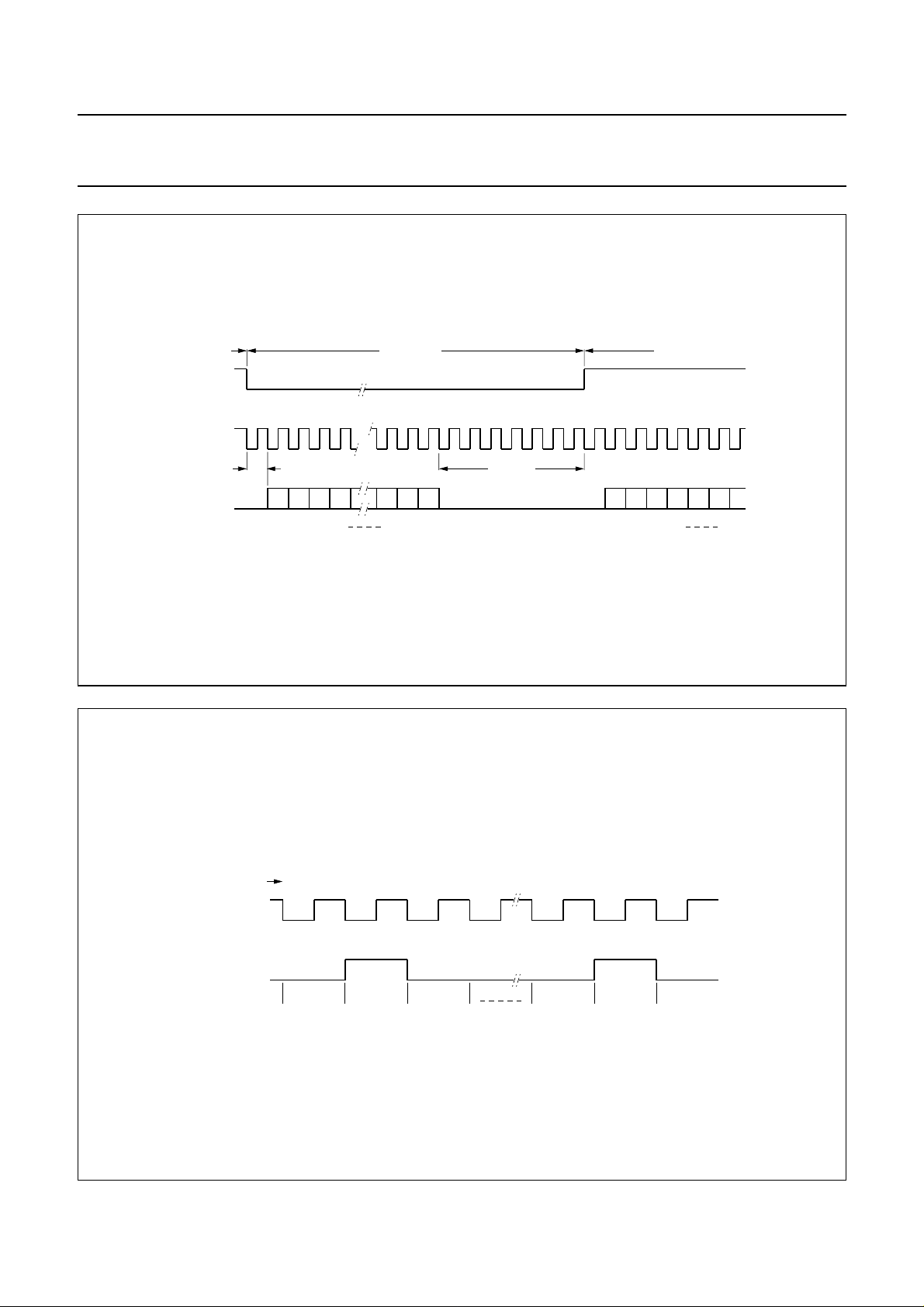
t
FRESET
t
suD
FDIR
TrH> 5T
TsD < 0 ns min. set-up time FDIR to FRESET = LOW
= 210 ns (for CLK24 = 24.576 MHz) min. time FRESET HIGH
CLK24
Fig.4 Timing: FRESET and FDIR.
August 1993 7
rH
MBC123 - 1

Philips Semiconductors Preliminary specification
Masking threshold processor for MPEG
layer 1 audio compression applications
Power-down Mode Switching
When the potential on the RESET pin (pin 23) is held HIGH
for at least 5T
after which it will operate in its decoding mode.
The power-down mode is activated when the PWRDWN
pin (pin 30) is held HIGH. The 3-state buffers will be set to
a high impedance while the normal outputs will retain the
state attained prior to this mode being entered. This mode
can only be used if other associated circuits react
accordingly. The power-down mode is de-activated by a
reset action.
Fig.5 shows the operation for the power-down mode
switching.
clock periods, the device will be reset
CLK24
SAA2521
Table 1 Resolution selection.
RESOL1 RESOL0 RESOLUTION
0 0 16-bits
0 1 18-bits
1 0 14-bits
1 1 15-bits
TrH> 5T
PWRDWN
RESET
= 210 ns (for CLK24 = 24.576 MHz) minimum time RESET HIGH
CLK24
Fig.5 Power-down mode switching.
sleep mode active
t
rH
MEA659 - 1
August 1993 8
Philips Semiconductors Preliminary specification
Masking threshold processor for MPEG
layer 1 audio compression applications
channel
SWS
SCL
FDA
bit :
1
0
msb lsb
left 32 bits
2102322212
7 bits
2322212
msb
right
0
SAA2521
MBC149 - 1
channel
SWS
FSYNC
sub-band
Fig.6 Format for transferring filtered data.
LRLLLLLLRRRRRR
31 0 1 31 0 1
MBC126 - 2
Fig.7 FSYNC related to SWS 0 data transfer period.
August 1993 9
 Loading...