

Philips SAA2510 Datasheet

INTEGRATED CIRCUITS
DATA SH EET
SAA2510
Video CD (VCD) decoder
Preliminary specification
File under Integrated Circuits, IC02
1996 May 21

Philips Semiconductors Preliminary specification
Video CD (VCD) decoder SAA2510
FEATURES
(With standard microcode loaded)
• Decoding and display of MPEG1 video streams
(constrained parameters)
• Decoding of MPEG audio streams (layer II)
• Decoding, storage (compressed) and display of
high-resolution still pictures of 704 × 576 pixels
• Requires only 4 Mbits of external 70 ns DRAM
• Audio transparency mode for CD-DA discs
• On-screen display capability
• Play options:
– Play
– Stop
– Pause/continue
– Slow-motion forward
– Scan forward
– Scan backward.
• Supports auto-pause feature
2
• Disc interface: Philips I
S, EIAJ, MEC formats and
IEC 958 (EBU) interface
• Separate error flag input (EFIN) and data valid input
(NDAV)
• Performs basic block decoder functions:
– serial-to-parallel conversion
– sync detection
– descrambling
– EDC calculation
– error-correction for mode 2 form 1 sectors
– header and sub-header interpretation.
• I2C-bus interface
• Video output YUV 4:2:2 format. DMSD bus
compatible
• Also supports CCIR656 video interface, including line
and field timing codes
• Audio output: 44.1 kHz. 16, 18 or 20 bits per audio
sample in Philips I2S, Sony or MEC formats
• EBU audio output, fully transparent from input to output
in CD-DA mode and generated in MPEG mode
• Downloadable microcode for internal controllers
• Internal video timing generator
• Requires 40 MHz crystal for system clock generation
• Requires 27 MHz crystal or external 27 MHz source for
video timing generation
• Requires 16.9344 MHz (384 × 44.1 kHz) clock locked to
CD drive
• Internal generation of 90 kHz MPEG clock
• Capability of sharing external DRAM by 3-stating all
DRAM pins.
APPLICATION
• Dedicated video CD players.
GENERAL DESCRIPTION
MPEG1 audio and video CD (VCD) decoder, intended for
use in low-cost dedicated video CD players. When used
with a 4 Mbit DRAM and a digital video encoder, the
decoder adds the required functionality to a CD decoder to
implement a low-cost video CD player capable of playing
discs coded to version 2.0 of the video CD specification.
The SAA2510 is an I
2
C-bus controlled chip and features
serial data input in four common bus formats. It provides
digital video output in CCIR601 and 656 formats.
A bit-mapped on-screen display is provided and output
video timing can be 525 lines/30 frames per second or
625 lines/25 frames per second. The chip is microcode
programmable for feature enhancement.
ORDERING INFORMATION
PACKAGE
TYPE NUMBER
NAME DESCRIPTION VERSION
SAA2510 QFP100 plastic quad flat package; 100 leads (lead length 1.95 mm);
body 14 × 20 × 2.7 mm; high stand-off height
1996 May 21 2
SOT317-1

Philips Semiconductors Preliminary specification
Video CD (VCD) decoder SAA2510
QUICK REFERENCE DATA
SYMBOL PARAMETER MIN. TYP. MAX. UNIT
V
V
I
DD
f
xtal s
f
xtal v
f
i
T
DD3
DD5
amb
supply voltage 3.0 3.3 3.6 V
supply voltage 4.5 5.0 5.5 V
supply current − tbf − mA
system clock crystal frequency − 40.0 − MHz
video clock crystal frequency − 27.0 − MHz
audio clock input frequency − 16.9344 − MHz
operating ambient temperature −20 −+70 °C
1996 May 21 3
1996 May 21 4
a
ndbook, full pagewidth
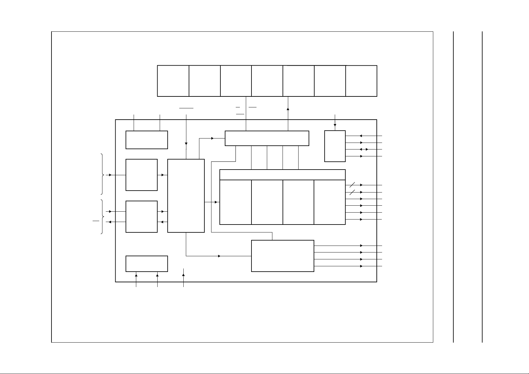
BLOCK DIAGRAM
Philips Semiconductors Preliminary specification
Video CD (VCD) decoder SAA2510
EBUIN
AUDIOCLK
WSIN
CLIN
EFIN
DAIN
NDAV
SDA
SCL
INT
ASEL
EXTERNAL
4 Mbit DRAM
Sys_osc_1 Sys_osc_0
76
SYSTEM CLOCK
BLOCK
DECODER
HOST
2
I
C
INTERFACE
BUFFER
74 27 79
SAA2510
TEST CONTROL
OSD
3 k 7 k
RESET CDIR
SYSTEM
CONTROLLER
PLAY
CONTROL
BUFFER
AUDIO
FIFO
W
RAS
MEMORY MANAGEMENT UNIT
DATA
SORTER
VIDEO
FIFO
CAS
A0 to A8 DR0 to DR15
VIDEO DECODER
IDCT
AUDIO DECODER
VIDEO
BUFFER
0
FRAME
RECON-
STRUCTOR
VIDEO
BUFFER
1
VIDEO
CLOCK
VIDEO
GENERATOR
VIDEO
BUFFER
2
8
95 to 88
8
7 to 1
100
84
86
82
80
99
97
11
9
12
13
16
14
Vid_osc_0
Vid_osc_1
CLK27
CREF
UV0 to UV7
Y0 to Y7
VSYNC
HREF
TLSAND
CSYNC
EBUOUT
DAOUT
CLOUT
WSOUT
77 78 28
TP1 TP2 DRAMON
MGE325
Fig.1 Block diagram.

Philips Semiconductors Preliminary specification
Video CD (VCD) decoder SAA2510
PINNING
SYMBOL PIN DESCRIPTION
UV6 1 video UV bus output bit 6;
16-bit video output mode: the UV bus outputs alternating U and V chroma samples
at 13.5 Mbytes/s
CCIR656 mode: this bus is not used (inactive)
UV5 2 video UV bus bit 5
UV4 3 video UV bus bit 4
UV3 4 video UV bus bit 3
UV2 5 video UV bus bit 2
UV1 6 video UV bus bit 1
UV0 7 video UV bus bit 0
V
DD5
CSYNC 9 composite sync output; 525 lines/60 Hz or 625 lines/50 Hz
V
SS5
TLSAND 11 two-level Sandcastle (composite blanking) output; requires external resistor network
EBUOUT 12 IEC 958 digital audio output
DAOUT 13 I
WSOUT 14 I
V
DD3
CLOUT 16 I
V
SS
AUDIOCLK 18 16.9 MHz audio clock input
V
DD5
EBUIN 20 EBU (IEC 958) input
CLIN 21 I
WSIN 22 I
DAIN 23 I
V
DD3
EFIN 25 error flag input from I
V
SS
RESET 27 active low reset input
DRAMON 28 DRAM pin 3-state control input; also 3-states video outputs and some timing signals
INT 29 active low open drain interrupt request to host microcontroller
NDAV 30 data not valid input (data on I
ASEL 31 I
SDA 32 I
V
DD5
SCL 34 I
V
SS5
DR15 36 DRAM data input/output bit 5
8 5 V external pad power supply
10 0 V external pad power supply
to define horizontal/vertical blanking level
2
S data; digital audio output
2
S word select digital audio output
15 +3 V internal power supply
2
S bit clock output
17 0 V internal power supply
19 5 V internal power supply
2
S bit clock input
2
S word select input
2
S digital data input
24 +3 V internal power supply
2
S source
26 0 V internal power supply
2
C-bus address select pin
2
C-bus data pin
33 5 V external pad power supply
2
C-bus clock input
35 0 V external pad power supply
2
S or EBU input not valid)
1996 May 21 5
Philips Semiconductors Preliminary specification
Video CD (VCD) decoder SAA2510
SYMBOL PIN DESCRIPTION
DR14 37 DRAM data input/output bit 14
DR13 38 DRAM data input/output bit 13
DR12 39 DRAM data input/output bit 12
DR11 40 DRAM data input/output bit 11
DR10 41 DRAM data input/output bit 10
DR9 42 DRAM data input/output bit 9
V
DD5
DR8 44 DRAM data input/output bit 8
V
SS5
DR7 46 DRAM data input/output bit 7
DR6 47 DRAM data input/output bit 6
DR5 48 DRAM data input/output bit 5
DR4 49 DRAM data input/output bit 4
DR3 50 DRAM data input/output bit 3
DR2 51 DRAM data input/output bit 2
DR1 52 DRAM data input/output bit 1
DR0 53 DRAM data input/output bit 0
V
SS5
CAS 55 DRAM column address strobe
V
DD5
A8 57 DRAM row/column address pin A8
A7 58 DRAM row/column address pin A7
A6 59 DRAM row/column address pin A6
A5 60 DRAM row/column address pin A5
A4 61 DRAM row/column address pin A4
V
DD3
W 63 active low DRAM write strobe
V
SS
RAS 65 DRAM row address strobe
V
DD5
A3 67 DRAM row/column address pin A3
V
SS5
A2 69 DRAM row/column address pin A2
V
DD5
A1 71 DRAM row/column address pin A1
A0 72 DRAM row/column address pin A0
V
DDO3
Sys_osc_0 74 oscillator input pin; 40 MHz oscillator
V
SS
Sys_osc_1 76 oscillator output pin; 40 MHz oscillator
TP1 77 factory test pin; connect to ground
43 5 V external pad power supply
45 0 V external pad power supply
54 0 V external pad power supply
56 5 V external pad power supply
62 +3 V internal power supply
64 0 V internal power supply
66 5 V internal power supply
68 0 V external pad power supply
70 5 V external pad power supply
73 3 V internal power supply for oscillator
75 0 V internal power supply
1996 May 21 6

Philips Semiconductors Preliminary specification
Video CD (VCD) decoder SAA2510
SYMBOL PIN DESCRIPTION
TP2 78 factory test pin; connect to ground
CDIR 79 clock direction control pin; when high, CLK27 is an output
CREF 80 clock qualifier output; 13.5 MHz timing signal used in 16-bit video output mode; can
also be used as 13.5 MHz video sample clock
V
SS5
CLK27 82 27 MHz clock input or output; direction controlled by CDIR pin
V
DD5
Vid_osc_0 84 oscillator pin; 27 MHz; input pin
V
SS
Vid_osc_1 86 oscillator pin; 27 MHz; output pin
V
DDO3
Y7 88 video Y bus output bit 7
Y6 89 video Y bus bit 6
Y5 90 video Y bus bit 5
Y4 91 video Y bus bit 4
Y3 92 video Y bus bit 3
Y2 93 video Y bus bit 2
Y1 94 video Y bus bit 1
Y0 95 video Y bus bit 0
V
SS5
HREF 97 horizontal (line) timing reference signal; high during active video part of line, low
V
DD5
VSYNC 99 vertical (field/frame) timing reference signal; high during vertical blanking interval of
UV7 100 video UV bus output bit 7
81 0 V external pad power supply
83 5 V external pad power supply
85 0 V internal power supply
87 3 V internal power supply for oscillator
DMSD mode: the Y bus outputs luminance samples at 13.5 Mbytes/s
CCIR656 mode: this pin supplies multiplexed chrominance and luminance
(27 Mbytes/s)
96 0 V external pad power supply
during line blanking
98 5 V external pad power supply
field
DMSD mode: the UV bus outputs alternating U and V chroma samples at
13.5 Mbytes/s
CCIR656 mode: this bus is not used (inactive)
1996 May 21 7
Philips Semiconductors Preliminary specification
Video CD (VCD) decoder SAA2510
handbook, full pagewidth
DD5
UV6
UV5
UV4
UV3
UV2
UV1
UV0
V
DD5
CSYNC
V
SS5
TLSAND
EBUOUT
DAOUT
WSOUT
V
DD3
CLOUT
V
SS
AUDIOCLK
V
DD5
EBUIN
CLIN
WSIN
DAIN
V
DD3
EFIN
V
SS
RESET
DRAMON
INT
NDAV
UV7
VSYNC
99989796959493929190898887868584838281
100
1
2
3
4
5
6
7
8
9
10
11
12
13
14
15
16
17
18
19
20
21
22
23
24
25
26
27
28
29
30
SS5
V
HREF
V
Y0Y1Y2Y3Y4Y5Y6Y7V
SAA2510
DDO3
Vid_osc_1
DD5
VSSVid_osc_0
V
CLK27
V
SS5
80
79
78
77
76
75
74
73
72
71
70
69
68
67
66
65
64
63
62
61
60
59
58
57
56
55
54
53
52
51
CREF
CDIR
TP2
TP1
Sys_osc_1
V
SS
Sys_osc_0
V
DDO3
A0
A1
V
DD5
A2
V
SS5
A3
V
DD5
RAS
V
SS
W
V
DD3
A4
A5
A6
A7
A8
V
DD5
CAS
V
SS5
DR0
DR1
DR2
31323334353637383940414243444546474849
SS5
SCL
DD5
ASEL
SDA
V
DR15
DR14
DR13
V
DR12
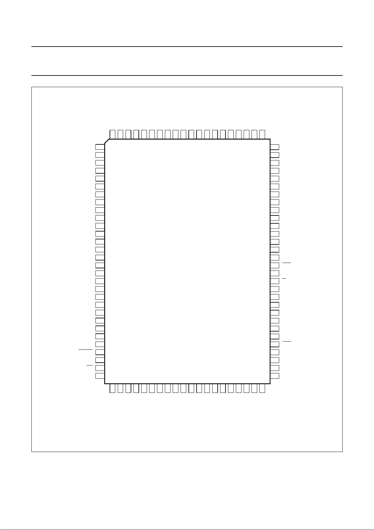
Fig.2 Pin configuration.
1996 May 21 8
DR11
DR10
DR9VDD5
DR8
SS5
V
DR7
DR6
DR5
DR4
50
DR3
MGE324

Philips Semiconductors Preliminary specification
Video CD (VCD) decoder SAA2510
FUNCTIONAL DESCRIPTION
Block decoder
The VCD chip receives MPEG A/V or CD digital audio data
from a CD decoder chipset using any one of four common
interface formats (Philips I
Philips I2S, EIAJ and Matsushita input modes use the bit
clock (CLIN), word select (WSIN), data (DAIN) and error
flag (EFIN) inputs. If IEC 958 (EBU) input mode is
selected, only the EBUIN pin needs to be connected. The
chip also requires a 16.9 MHz clock input (CLIN) which is
synchronous with the data input from the CD decoder
providing the serial data input.
The VCD chip contains a block decoder and descrambler
which performs error correction on the Video CD data track
(form 1) sectors and error detection on real-time audio and
video tracks where an error correction code is present.
In most events, audio output can be in any of the three
(I2S, EIAJ or MEC) formats, independent of input type.
When playing CD digital audio discs, the input is copied to
the outputs.
The block decoder supports some special functions which
enable recovery of play control lists. The desired sectors
can be acquired by programming a sector address via the
I2C-bus microcontroller interface. The microcontroller then
instructs the CD servo/decoder subsystem to execute a
servo jump to the required disc location and then waits for
an interrupt indicating that the desired sector information
has been received and error-corrected.
System controller
Overall control of the chip and a number of its less
time-critical functions is carried out by a dedicated
RISC processor. The microcode for this processor is
executed from an on-chip RAM. This microcode must be
loaded into RAM after power-up by the host
microcontroller, using the I
the functionality of the chip to be customized for specific
applications.
On-screen display
The VCD chip provides a bit-mapped On-Screen-Display
(OSD), containing 32 display lines of 352 pixels per line.
There is a double-height mode which repeats OSD lines so
that the maximum height of OSD objects becomes
64 lines. This character-set-independent OSD permits
display of ideographic characters and simple graphic
displays anywhere on the screen.
2
S, EIAJ, MEC or IEC 958). The
2
C-bus interface. This enables
The OSD is implemented as 48 vertical ‘slices’ of 8 pixels
(horizontally) and 32 (vertically). Each pixel is stored as
2 bits. This gives three programmable logical colours, plus
a transparent option. Each slice is identified by a slice code
(slice number).
The horizontal position of a slice is defined by its position
in a slice code sequence written to the VCD chip. This
arrangement reduces the need to completely update the
OSD bit map in many situations. It may be possible to
simply reorder the slices, e.g. if a track time display is
being updated and slices are prepared to represent digits.
At any time, up to 44 of the 48 slices can be displayed.
Video decoder
Video output data can be presented in one of two modes:
1. 16-bit wide data is output in YUV 4 : 2 : 2 format as
8 bits of luminance and 8 bits of alternating U and
V chrominance. The video output data rate in this
mode is 13.5 Mwords/s.
2. 8-bit wide, CCIR656-like, data is output providing
4:2:2 format video as an 8-bit UYVY multiplex at
27 Mbytes/s.
In either case, the VCD chip can be programmed to output
525 line or 625 line format timing to match the type of
display (TV) connected to its output. Additional
programmability is provided to cope with the Video CD disc
source picture coding type (525/625 lines).
The VCD chip performs vertical and horizontal
interpolation to convert the MPEG SIF (352 pixels per line)
normal resolution pictures to CCIR601 resolution.
Vertically interpolated pixels are output on the odd fields
during display of normal resolution pictures.
The Video CD disc being played may have been coded
with 525 lines/60 Hz or 625 lines/50 Hz pictures. When the
Video CD player is connected to a display with a different
timebase to the coded disc material, some adjustments
must be made to allow for the different number of lines on
the display and the reconstructed picture. Two examples
are shown in Figs. 3 and 4.
The VCD chip can be programmed to position the
reconstructed picture with respect to horizontal and
vertical syncs anywhere on the display screen with a
programmable ‘viewport’ position. Figure 3 shows an
MPEG SIF resolution picture (352 pixels by 288 lines)
being displayed on an NTSC display having only
240 active display lines per field. In this event, the top and
bottom 24 lines are not displayed.
1996 May 21 9
 Loading...