

Philips SA647DH, SA647DK Datasheet

SA647
Low-voltage digital IF receiver
Product specification 1998 Aug 10
INTEGRATED CIRCUITS
Philips Semiconductors Product specification
SA647Low-voltage digital IF receiver
2
1998 Aug 10 853–2037 19849
DESCRIPTION
The SA647 is a low-voltage high performance monolithic digital
system with high-speed RSSI incorporating a mixer, oscillator with
buffered output, two limiting intermediate frequency amplifiers, fast
logarithmic received signal strength indicator (RSSI), voltage
regulator, RSSI op amp and power down pin. The SA647 is
available in TSSOP (thin shrink small outline package).
The SA647 was designed for portable digital communication
applications and will function down to 2.7V . The limiter amplifier has
differential outputs with 2MHz small signal bandwidth. The RSSI
output has access to the feedback pin. This enables the designer to
level adjust the outputs or add filtering.
FEA TURES
•V
CC
= 2.7 to 5.5V
•Low power receiver (5.3mA @ 3V)
•Power down mode (I
CC
= 110µA)
•Fast RSSI rise and fall times
•Extended RSSI range with temperature compensation
•RSSI op amp
•2MHz limiter small signal bandwidth
•Filter matching (1.5kΩ)
•Differential limiter output
•Oscillator buffer
•TSSOP-20 package
APPLICA TIONS
•NADC (North American Digital Cellular)
•Digital receiver systems
•Cellular radio
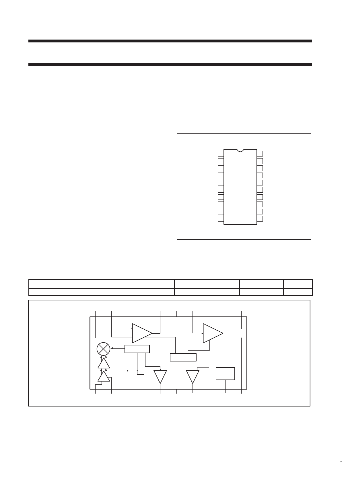
PIN CONFIGURATION
SR01456
MIX
OUT
IF AMP
IN
GND
LIM
IN
LIM OUT (+)
RF
IN+
RF
IN–
OSC E
OSC B
OSC
BUF
OUT
RSSI
RSSI FB
P
D
1
2
3
4
5
6
7
8
9
10
11
12
13
14
20
19
18
17
16
15
LIM OUT (-)
V
CC
IF AMP
DECOUP
IF AMP
DECOUP
IF AMP
OUT
LIM
DECOUP
LIM
DECOUP
Figure 1. Pin Configuration
ORDERING INFORMATION
DESCRIPTION TEMPERATURE RANGE ORDER CODE DWG #
20-Pin Plastic Thin Shrink Small Outline Package (Surface-mount) –40 to +85°C SA647DH SOT360–1
SR01727
OSCILLATOR
MIXER
+–
IF
AMP
20 19 18 17 16 15 14 13 12 11
123 45678 910
EB
LIMITER
V
CC
GND
FAST RSSI
+–
POWER
DOWN
Figure 2. Block Diagram
Philips Semiconductors Product specification
SA647Low-voltage digital IF receiver
1998 Aug 10
3
PIN DESCRIPTION
PIN NO. SYMBOL FUNCTION
1 RF
IN
RF input
2 RF BYPASS RF bypass
3 OSC
E
Oscillator emitter
4 OSC
B
Oscillator base (input)
5 OSC
BUF
OUT Oscillator buffer output
6 V
CC
Supply voltage
7 RSSI RSSI output
8 RSSI FB RSSI Feedback
9 P
D
Power Down
10 LIM
OUT(–)
Limiter output (neg)
11 LIM
OUT(+)
Limiter output (pos)
12 LIM
DECOUP
Limiter decoupling
13 LIM
DECOUP
Limiter decoupling
14 LIM
IN
Limiter input
15 GND Ground
16 IF AMP
OUT
IF amplifier output
17 IF AMP
DECOUP
IF amplifier decoupling
18 IF AMP
IN
IF amplifier input
19 IF AMP
DECOUP
IF amplifier decoupling
20 MIX
OUT
Mixer output
Philips Semiconductors Product specification
SA647Low-voltage digital IF receiver
1998 Aug 10
4
ABSOLUTE MAXIMUM RATINGS
SYMBOL PARAMETER RATING UNITS
V
CC
Supply voltage -0.3 to +6.0 V
V
IN
Voltage applied to any other pin -0.3 to (VCC + 0.3) V
T
STG
Storage temperature range -65 to +150
°C
T
A
Operating ambient temperature range -40 to +85
°C
NOTE: Thermal impedance (θJA) = 135°C/W
DC ELECTRICAL CHARACTERISTICS
VCC = +3.0V , TA = 25°C; unless otherwise stated.
LIMITS
SYMBOL
PARAMETER
TEST CONDITIONS
MIN TYP MAX
UNITS
V
CC
Power supply voltage range 2.7 5.5 V
I
CC
DC current drain 4 5.3 7 mA
Standby Pin 9 = LOW 0.11 mA
Input current Pin 9 = LOW -10 10
Pin 9 = HIGH -10 10
µ
A
Input level Pin 9 = LOW 0 0.3V
CC
Pin 9 = HIGH 0.7 V
CC
V
CC
V
τ
on
Power–up time RSSI valid (10% to 90%) 10
sec
τ
off
Power–down time RSSI valid (90% to 10%) 5
sec
Philips Semiconductors Product specification
SA647Low-voltage digital IF receiver
1998 Aug 10
5
AC ELECTRICAL CHARACTERISTICS
VCC = +3.0V , Mixer input freq = 110.52MHz, LO input freq = 109.92MHz, TA = 25°C; unless otherwise stated.
LIMITS
SYMBOL
PARAMETER
TEST CONDITIONS
MIN TYP MAX
UNITS
Mixer/Osc section
f
IN
Input signal frequency 200 MHz
f
OSC
Crystal oscillator frequency 200 MHz
NF Noise figure at 110.52MHz Matched input and output 50Ω 4.5 dB
IIP3 Third-order input intercept point Matched input and output to 50Ω -29.5 dBm
G
CP
Conversion power gain Matched input and output to 50Ω 17 20 23 dB
R
IN
Mixer input resistance at 110.52 MHz 670 Ω
C
IN
Mixer input capacitance at 110.52 MHz 3.0 pF
R
OUT
Mixer output resistance at 600 kHz 1.5 kΩ
I
SOL
Mixer RF to LO isolation 32 dB
Buffered LO output level, DC coupled 10kII3.9pF load 110 230 320 mV
P–P
External input level f = 110.52 MHz at Pin 4 250 mV
P–P
IF section
IF amp power gain
Matched input and output 50W
30 36 dB
Limiter power gain 51 60 dB
IF
BW
IF amp bandwidth 2 MHz
RSSI output Input power level = -113dBm, Pin 1 0.30 V
Input power level = -68dBm, Pin 1 1.00 V
Input power level = -29dBm, Pin 1 1.55 V
RSSI range 85 dB
RSSI accuracy ±1.5 dB
RSSI ripple 30 mV
P–P
RSSI speed – (Rise Time)
Input @ Pin 1 No filter
5 µs
RSSI speed – (Fall time)
Input @ Pin 1
No filter 25 µs
IF input impedance 1.5 kΩ
IF output impedance 1.5 kΩ
Limiter input impedance 1.5 kΩ
Limiter output impedance (Pin 10, Pin 11) 230 Ω
Limiter output (each pin)
Output load is 1.5K in parallel with 30
pF to GND each pin
240 350 420 mV
P–P
Limiter output DC level 1.27 V
Differential output matching ±5 mV
Limiter output offset 0.09 V
 Loading...