

Philips SA639DH Datasheet

INTEGRATED CIRCUITS
SA639
Low voltage mixer FM IF system with
filter amplifier and data switch
Product specification 1998 Feb 10
IC17 Data Handbook

Philips Semiconductors Product specification
Low voltage mixer FM IF system with filter amplifier
and data switch
DESCRIPTION
The SA639 is a low-voltage high performance monolithic FM IF
system with high-speed RSSI incorporating a mixer/oscillator, two
wideband limiting intermediate frequency amplifiers, quadrature
detector, logarithmic received signal strength indicator (RSSI), fast
RSSI op amps, voltage regulator, wideband data output, post
detection filter amplifier and data switch. The SA639 is available in
24-lead TSSOP (Thin shrink small outline package).
The SA639 was designed for high bandwidth portable
communication applications and will function down to 2.7V . The RF
section is similar to the famous NE605. The data output provides a
minimum bandwidth of 1MHz to demodulate wideband data. The
RSSI output is amplified and has access to the feedback pin. This
enables the designer to level adjust the outputs or add filtering.
The post-detection amplifier may be used to realize a low pass filter
function. A programmable data switch routes a portion of the data
signal to an external integration circuit that generates a data
comparator reference voltage.
SA639 incorporates a power down mode which powers down the
device when Pin 8 is high. Power down logic levels are CMOS and
TTL compatible with high input impedance.
APPLICATIONS
•DECT (Digital European Cordless Telephone)
•FSK and ASK data receivers
FEATURES
•V
= 2.7 to 5.5V
CC
•Low power consumption: 8.6mA typ at 3V
•Wideband data output (1MHz min.)
•Fast RSSI rise and fall times
•Mixer input to >500MHz
•Mixer conversion power gain of 9.2dB and noise figure of 11dB at
110MHz
PIN CONFIGURATION
RF BYPASS
XTAL OSC (EMITTER)
XTAL OSC (BASE)
RSSI FEEDBACK
RSSI OUT
POWER DOWN CONTROL
DATA OUT
POSTAMP IN
POSTAMP OUT
SWITCH CONTROL
•XTAL oscillator effective to 150MHz (L.C. oscillator to 1GHz local
oscillator can be injected)
•92dB of IF Amp/Limiter power gain
•25MHz limiter small signal bandwidth
•Temperature compensated logarithmic Received Signal Strength
Indicator (RSSI) with a dynamic range in excess of 80dB
•RSSI output internal op amp
•Post detection amplifier for filtering
•Programmable data switch
•Excellent sensitivity: 2.24µV into 50Ω matching network for 10dB
SNR (Signal to Noise Ratio) with RF at 110MHz and IF at 9.8MHz
•ESD hardened
•Power down mode
RF
1
IN
2
3
4
5
V
CC
6
7
8
9
10
11
12
24
23
22
21
20
19
18
17
16
15
14
13
Figure 1. Pin Configuration
SA639
MIXER OUT
IF AMP DECOUPLING
IF AMP IN
IF AMP DECOUPLING
IF AMP OUT
GND
LIMITER IN
LIMITER DECOUPLING
LIMITER DECOUPLING
LIMITER OUT
QUADRATURE IN
SWITCH OUT
SR00030
ORDERING INFORMATION
DESCRIPTION TEMPERATURE RANGE ORDER CODE DWG #
24-Pin Plastic TSSOP (Thin Shrink Small Outline Package) -40 to +85°C SA639DH
1998 Feb 10 853-1792 18944
2
SOT-355
Philips Semiconductors Product specification
Input current
A
Input level
Input current
A
Low voltage mixer FM IF system with filter amplifier
and data switch
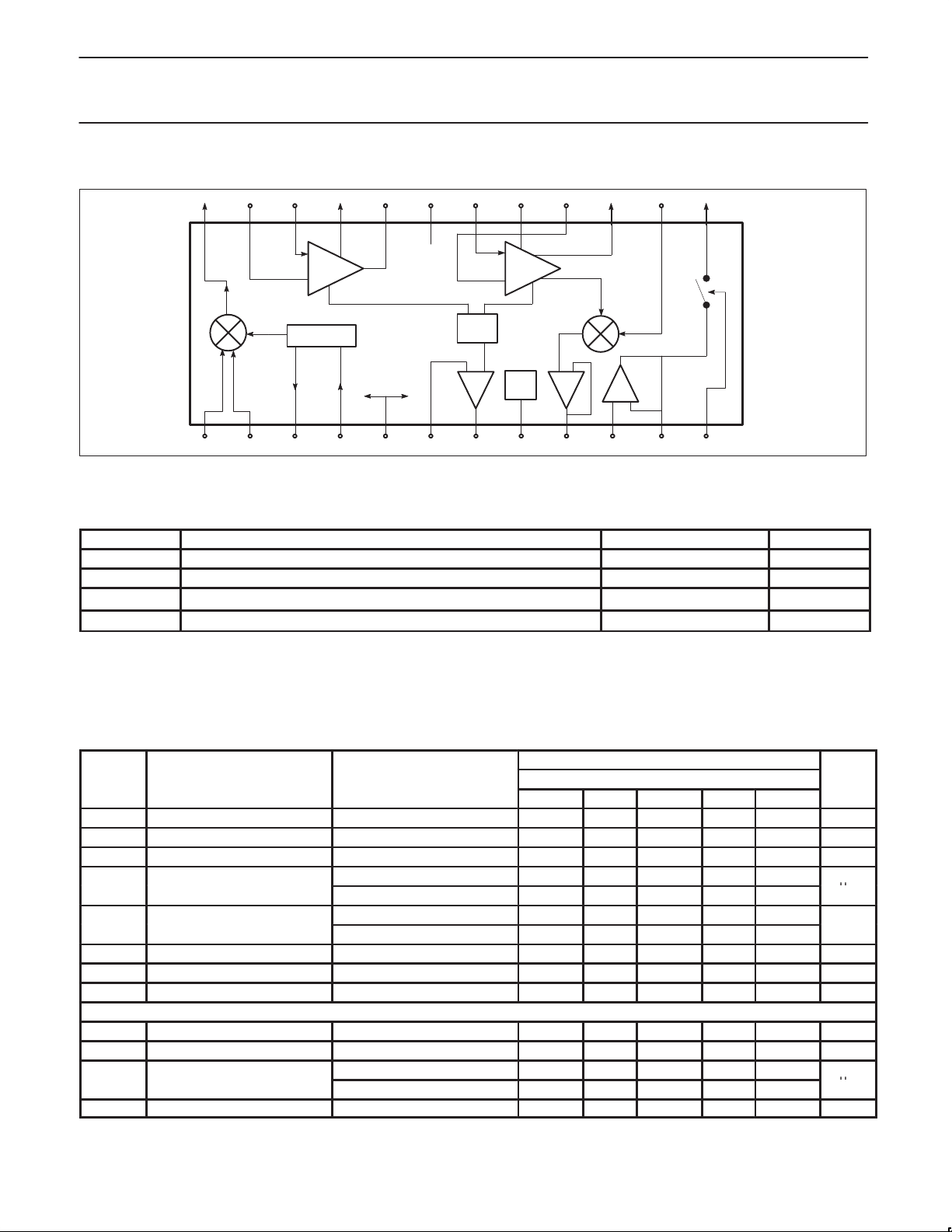
BLOCK DIAGRAM
23 22
IF
AMP
MIXER
OSCILLATOR
EB
ABSOLUTE MAXIMUM RATINGS
SYMBOL PARAMETER RATING UNITS
V
CC
V
IN
T
STG
T
A
NOTE:
1. Except logic input pins (Pins 8 and 12) which can have 6V maximum.
Thermal impedance (DH package) 117°C/W
2. θ
JA
Single supply voltage -0.3 to 6 V
Voltage applied to any other pin
Storage temperature range -65 to +150
Operating ambient temperature range SA639
20 19 18 17 16 15 14 132124
GND
V
CC
RSSI
Figure 2. Block Diagram
1
2
FAST
RSSI
+–
LIMITER
PWR
DWN
DATA
QUAD
+–
+–
10987654321
1211
-0.3 to (VCC+0.3) V
-40 to +85
SA639
SR00031
°C
°C
DC ELECTRICAL CHARACTERISTICS
VCC = +3V, TA = 25°C; unless otherwise stated.
LIMITS
SYMBOL PARAMETER TEST CONDITIONS SA639 UNITS
MIN -3σ TYP +3σ MAX
V
I
I
t
t
OFF
NOTE:
1. When the device is forced in power down mode via Pin 8, the Data Switch will output a voltage close to 1.6V and the state of the switch
control input will have no effect.
Power supply voltage range 2.7 3.0 5.5 V
CC
DC current drain Pin 8 = LOW, Pin 12 = HIGH 8.33 8.6 8.87 10 mA
CC
Standby Pin 8 = HIGH, Pin 12 = HIGH 131.9 140 148.1 500 µA
CC
p
p
Power up time RSSI valid (10% to 90%) 10 µs
ON
Pin 8 = LOW 10
Pin 8 = HIGH 4
Pin 8 = LOW 0 0.3V
Pin 8 = HIGH
NO TAG
0.7V
CC
Power down time RSSI invalid (90% to 10%) 5 µs
Power up settling time Data output valid 100 200 µs
Switch closed Pin 12 = LOW, PIN 8 = LOW 0 0.3 V
Switch open (output tri-state) Pin 12 = HIGH 0.7 V
p
Pin 12 = LOW 10
Pin 12 = HIGH 4
CC
Switch activation time 0.5 1 µs
µ
CC
6
CC
6 V
µ
V
V
1998 Feb 10
3
Philips Semiconductors Product specification
s
s
Low voltage mixer FM IF system with filter amplifier
and data switch
AC ELECTRICAL CHARACTERISTICS
TA = 25°C; VCC = +3V, unless otherwise stated. RF frequency = 110.592MHz ;LO frequency = 120.392MHz; IF frequency = 9.8MHz; RF level
= -45dBm; FM modulation = 576kHz with ±288kHz peak deviation, discriminator tank circuit Q=4. The parameters listed below are tested using
automatic test equipment to assure consistent electrical characteristics. The limits do not represent the ultimate performance limits of the
device. Use of an optimized RF layout will improve many of the listed parameters.
LIMITS
SYMBOL PARAMETER TEST CONDITIONS SA639 UNITS
MIN -3σ TYP +3σ MAX
Mixer/Osc section (ext LO = -14dBm)
f
f
OSC
IF section
RF/IF section (ext LO = -14dBm)
S/N Signal-to-noise ratio No modulation for noise 56.1 60 63.9 dB
Input signal frequency 500 MHz
IN
External oscillator (buffer) 0.2 500 MHz
Noise figure at 110MHz 10.4 11 11.6 dB
Third-order input intercept point
Conversion power gain 6 8.6 9.2 11.1 dB
RF input resistance Single-ended input 800 Ω
RF input capacitance 3.5 pF
Mixer output resistance (Pin 24) 330 Ω
IF amp gain 38.86 40 41.14 dB
Limiter gain 50.44 52 53.56 dB
Input limiting -3dB Test at Pin 22 –100 dBm
IF input impedance 330 Ω
IF output impedance 330 Ω
Limiter input impedance 330 Ω
Limiter output impedance 300 Ω
Limiter output level with no
load
Data level RL = 10kΩ, CL = 30pF 260 360 mV
Data bandwidth 2.1 2.4 2.7 MHz
AM rejection 80% AM 1kHz 34.8 36 37.2 dB
RF RSSI output with buffer RF level = -45dBm 0.5 0.732 0.9 1.068 1.3 V
RF RSSI output rise time IF frequency = 9.8MHz
(10kHz pulse, w/ 9.8MHz filter) RF level = -45dBm 0.8
(no RSSI bypass capacitor) RF level = -28dBm 0.8
RF RSSI output fall time IF frequency = 9.8MHz
(10kHz pulse, w/ 9.8MHz filter) RF level = -45dBm 2.0
(no RSSI bypass capacitor) RF level = -28dBm 1.8
RSSI range 80 dB
RSSI accuracy ±1.5 dB
SINAD RF level = -85dBm 9.45 12 14.55 dB
S/N RF level = -100dBm 5.8 10 14.2 dB
Matched f1=110.592MHz;
f2=110.852MHz
RF level = -90dBm 0 0.232 0.4 0.568 0.75
RF level = -10dBm 0.8 1.032 1.2 1.368 1.6
-11 -9.5 -8 dBm
130 mV
SA639
RMS
P-P
µ
µ
1998 Feb 10
4
Philips Semiconductors Product specification
Dynamic offset voltage
2
6
mV
Low voltage mixer FM IF system with filter amplifier
and data switch
AC ELECTRICAL CHARACTERISTICS (Continued)
LIMITS
SYMBOL PARAMETER TEST CONDITIONS SA639 UNITS
MIN -3σ TYP +3σ MAX
Post detection filter amplifier
Amplifier 3dB bandwidth
Amplifier gain
Slew rate
Input resistance 300 kΩ
Input capacitance 3 pF
Output impedance 150 800 Ω
Output load resistance AC coupled 5 kΩ
Output load capacitance
DC output level
2
1
Data switch
DC input voltage range
3
AC input swing 400 mV
Input impedance 100 kΩ
Input capacitance 5 pF
Output load resistance 500 Ω
Through Mode (Pin 12 = LOW)
AC voltage gain
4
Output drive capability Sink/source, V
Slew rate V
Static offset voltage
5
,
Tri-State Mode (Pin 12 = HIGH)
Output leakage current V
NOTES:
1. Includes filter feedback capacitance, comparator input capacitance. PCB stray capacitances and switch input capacitance.
2. Demodulator output DC coupled with Post Detection Filter Amplifier input and the demodulator tank exactly tuned to center frequency.
3. Includes DC offsets due to frequency offsets between Rx and Tx carrier and demodulator tank offset due to mis-tuning.
4. With a 400mV
5. With a DC input and capacitor in the RC load fully charged.
sinusoid at 600kHz driving Pin 10. Output load resistance 500Ω in series with 10nF.
P-P
6. The switch is closed every 10ms for a duration of 40µs. The DC offset is determined by calculating the difference of 2 DC measurements,
which are determined as follows: 1) The first DC value is measured at the integrating capacitor of the switch when the switch is in the closed
position immediately before it opens. The value to be measured is in the middle of the peak-to-peak excursion of the superimposed
sine-wave. (DClow + (DChigh – DClow)/2). 2) The second DC value (calculated as above) is measured at Pin 11 immediately after the
switch opens, and is the DC value which gives the largest DC offset to the first DC measurement within a 400µs DECT burst. Minimum and
maximum limits are not tested, however, they are guaranteed by design and characterization using an optimized layout and application
circuit.
7. Standard deviations are measured based on application of 60 parts.
AC coupled: RL = 10kΩ,
C
= 33pF
L
AC coupled: RL = 10kΩ,
V
OUT DC
= 1.6V
AC coupled: RL = 10kΩ,
CL = 33pF
11.7 12.8 13.8 MHz
-0.2 dB
2.4 V/µs
AC coupled 30 pF
1.5 1.682 1.7 1.718 1.9 V
1.2 1.6 2.0 V
-1.5 dB
= 1.6V 3 mA
OUT DC
= 1.6V >14.0 V/µs
OUT DC
V
= 1.2 to 2.0V -0.6 0.30 1.2 ±5 mV
IN DC
V
= 1.4 to 2.0V;
IN DC
VCC = 3.0 to 5.0V;
-7 +7
RF level = -70 to -40 dBm
V
= 1.4 to 2.0V;
IN DC
VCC = 3.0 to 5.0V;
-10 +10
RF level = -40 to -5 dBm
= 1.2 to 2.0V 9.5 20 30.5 100 nA
OUT DC
SA639
P-P
1998 Feb 10
5
 Loading...