

Philips Semiconductors Preliminary specification
SA638IS-54 IF receiver
1
1995 Feb 16
DESCRIPTION
The SA638 is an IF receiver chip which serves the dual mode
functionality required by the IS–54 standards for North American
cellular telephones. It provides for both the analog FM (AMPS
mode) and DQPSK (TDMA digital mode) IF receive functions in a
monolithic BiCMOS Integrated Circuit housed in a compact
SSOP–24 plastic package.
APPLICATIONS
•
FEATURES
•
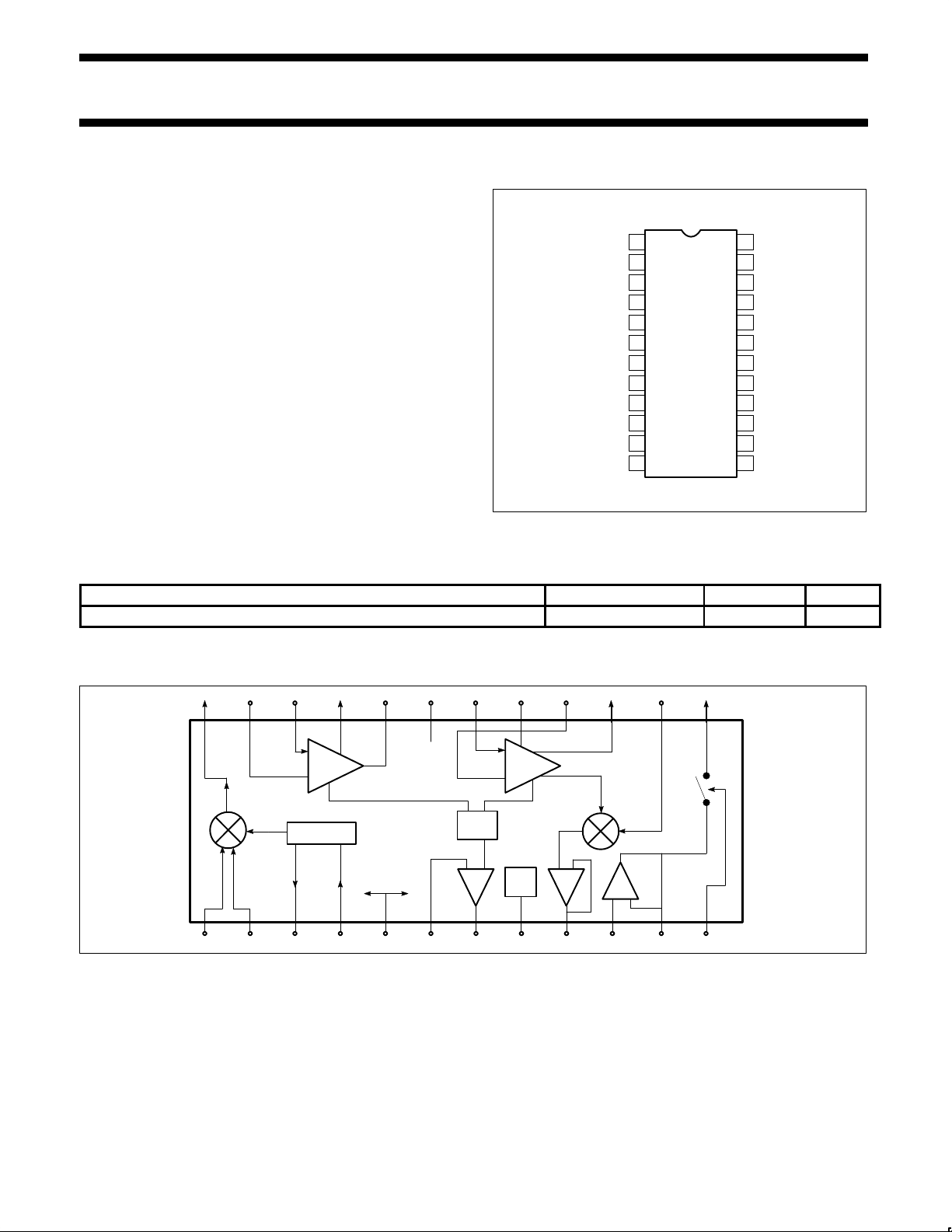
PIN CONFIGURATION
RF
IN
RF BYPASS
XTAL OSC (EMITTER)
XTAL OSC (BASE)
IF AMP DECOUPLING
IF AMP OUT
GND
LIMITER IN
SWITCH OUT
POWER DOWN CONTROL
POSTAMP IN
POSTAMP OUT
SWITCH CONTROL
MIXER OUT
IF AMP IN
LIMITER DECOUPLING
LIMITER DECOUPLING
LIMITER OUT
QUADRATURE IN
V
CC
RSSI FEEDBACK
RSSI OUT
DATA OUT
1
2
3
4
5
6
7
8
9
10
11
12
13
14
24
23
22
21
20
19
18
17
16
15
IF AMP DECOUPLING
UPDATE for 638
SR00907
Figure 1. Pin Configuration
ORDERING INFORMATION
DESCRIPTION TEMPERATURE RANGE ORDER CODE DWG #
24-Pin Plastic TSSOP (Thin Shrink Small Outline Package) -40 to +85°C SA638
SOT-355
BLOCK DIAGRAM
20 19 18 17 16 15 14 132124
10987654321
FAST
IF
AMP
E B
OSCILLATOR
MIXER
QUAD
+–
RSSI
GND
PWR
DWN
RSSI
DATA
V
CC
23 22
1211
LIMITER
+ –
+ –
UPDATE for 638
SR00908
Figure 2. Block Diagram
Philips Semiconductors Preliminary specification
SA638IS-54 IF receiver
1995 Feb 16
2
PIN DESCRIPTIONS
Pin
No.
Mnemonic Function
1 RF
IN(+)
RF Input Plus: Differential RF Plus input to mixer.
2 RF
IN(–)
RF Input Minus: Differential RF Minus input to mixer.
3 OSC
B
LO Oscillator Transistor Base: LO generator (Pins 3 and 4) with internal buffer to drive mixer differentially. Can
also be driven externally.
4 OSC
E
LO Oscillator Transistor Emitter: Pins 3 and 4 are used to form an oscillator with external components (tank,
varactor, etc.).
5 V
CC1
Supply Voltage 1: Voltage supply for mixer and main bias.
6 RSSI/AGC
RSSI Out and AGC Input: Dual use: RSSI output in AMPS mode (no internal opamp) and AGC input in QPSK
mode if needed. If no AGC, input will auto AGC to pre-defined fixed level for IQ outputs, in which case this pin
also serves as RSSI output.
7 PWRDWN Power-Down: Chip power-down input (CMOS compatible).
8 OSC
DEMOD
IF Oscillator Input (LO frequency x4): Oscillator input x4 for I/Q demodulation is needed for internally
generating quad LOs by division.
9 ModeSW Mode Switch: Logic control signal to select between AMPS and QPSK modes of operation.
10 AUDIO/LPF
Audio Out and LPF Corner Frequency Control: Dual Use: Audio output in the AMPS mode and LPF corner
frequency control in QPSK mode.
11 DEMOD1 Demod Auxiliary Pin: Used to implement FM demodulation in AMPS mode.
12 Q Baseband Q Ouptut: Quadrature baseband output referenced to IQ
REF
.
13 I Baseband I Output: In-phase baseband output referenced to IQ
REF
.
14 V
CC2
Supply Voltage 2: Voltage supply for IF amp and demodulator.
15 IQ
REF
I/Q Reference Voltage: Reference voltage for baseband I/Q outputs.
16 GND2 Ground 2: Ground common for IF amp and demodulator.
17 DEMOD2/Offsets
Demod Auxiliary Pin and I/Q Offset Control: Dual Use: In AMPS mode serves for FM demodulator; in QPSK
mode serves as I/Q offset control.
18 IQ DEMOD Input to the Demodulator: IF input to demodulator from AGC IF amp output.
19 GND1 Ground 1: Ground common for mixer and main bias.
20 IFAMP
OUT
IF Amplifier Output: IF amplifier output.
21 V
CCMID
VCC Midpoint Bypass: The internally generated VCC midpoint bias needs to be externally bypassed with a
suitable capacitor.
22 IFAMP
IN
Input to IF Amplifier: Input to IF Amplifier from mixer through external filter .
23 IFAMP
DC
Reference Input to IF Amp: External bypassing for low frequency feedback of IF amp to null DC offsets.
24 MIX
OUT
Output from Mixer: IF output from mixer to external BPF and IF amp.
ABSOLUTE MAXIMUM RATINGS
SYMBOL PARAMETER RATING UNITS
V
CC
Single supply voltage V
V
IN
Voltage applied to any other pin V
T
STG
Storage temperature range
°C
T
A
Operating ambient temperature range SA639
°C
NOTE: θJA Thermal impedance (DH package) 117°C/W
 Loading...