

Philips sa631 DATASHEETS

INTEGRATED CIRCUITS
SA631
1GHz low voltage LNA and mixer
Product specification
IC17 Data Handbook
1998 Jan 08

Philips Semiconductors Product specification
SA6311GHz low voltage LNA and mixer
DESCRIPTION
The SA631 is a combined low-noise BiCMOS amplifier, and mixer
designed for high-performance low-power communication systems
from 800-1000MHz. The low-noise preamplifier has a 1.7dB noise
figure at 881MHz with 15dB gain and an IP3 intercept of –7dBm at
the input. The gain is stabilized by on-chip compensation to vary
less than ±0.2dB over –40 to +85°C temperature range. The
wide-dynamic-range mixer has a 10dB noise figure and IP3 of
+3.3dBm at the input at 881MHz. The nominal current drawn from a
single 3V supply is 8.3mA. Additionally, the entire circuit can be
powered down to further reduce the supply current to less than
20µA.
FEATURES
•Low current consumption
•Outstanding gain and noise figure
•Excellent gain stability versus temperature and supply voltage
•LNA and mixer power down capability
•Designed in Philips state of the art BiCMOS QUBIC process
APPLICATIONS
•900MHz cellular and cordless front-end
•Spread spectrum receivers
•RF data links
•UHF frequency conversion
•Portable radio
PIN CONFIGURATION
PD1
PD2
GND
LO OUT
GND
GND
GND
GND
GND
GND
10
Figure 1. Pin Configuration
1
2
3
4
5
6
7
8
9
20
MIXER OUT
MIXER OUT
19
18
GND
17
MIXER IN
16
GND
LNA IN
15
GND
14
LNA OUT
13
12
V
CC
GND
11
SR00124
ORDERING INFORMATION
DESCRIPTION TEMPERATURE RANGE ORDER CODE DWG #
20-Pin Shrink Small Outline Package (Surface-mount, SSOP)
BLOCK DIAGRAM
OUT
MIXER
OUT
GND
MIXER
20 19 18 17 16
PD1 PD2 GND
MIXER
IN
43215
LO GND GND
OUT
Figure 2. SA631 Block Diagram
GND
GND
–40 to +85°C
LNA
IN GND
GND
LNA
OUT
V
CC
15 14 13 12 11
LNA
761098
GND GND
GND
SA631DK SOT266-1
SR01588
1998 Jan 08 853–2045 18847
2
Philips Semiconductors Product specification
SYMBOL
PARAMETER
TEST CONDITIONS
UNITS
SA6311GHz low voltage LNA and mixer
ABSOLUTE MAXIMUM RATINGS
SYMBOL PARAMETER RATING UNITS
V
T
P
T
CC
V
IN
P
D
JMAX
MAX
STG
Supply voltage
Voltage applied to any other pin –0.3 to (VCC + 0.3) V
Power dissipation, T
Maximum operating junction temperature 150 °C
Maximum power input/output +20 dBm
Storage temperature range –65 to +150 °C
NOTES:
1. Transients exceeding 8V on V
2. Maximum dissipation is determined by the operating ambient temperature and the thermal resistance,
3. Pins 19 and 20 are ESD sensitive (mixer outputs).
RECOMMENDED OPERATING CONDITIONS
SYMBOL PARAMETER RATING UNITS
T
V
CC
amb
T
J
Supply voltage 2.7 to 5.5 V
Operating ambient temperature range –40 to +85 °C
Operating junction temperature –40 to +105 °C
1
= 25°C (still air)
20-Pin Plastic SSOP 980 mW
θ
JA
amb
pin may damage product.
CC
: 20-Pin SSOP = 110°C/W
2
–0.3 to +6 V
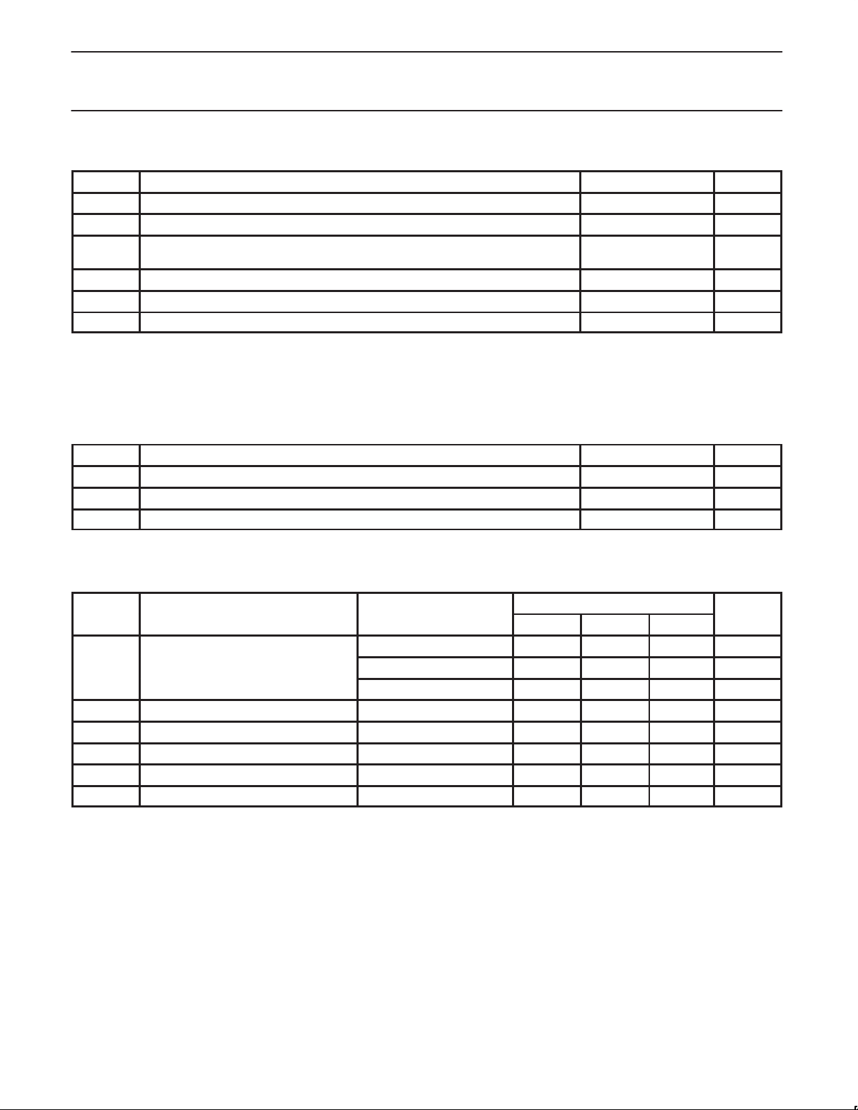
DC ELECTRICAL CHARACTERISTICS
VCC = +3.0V , T
I
CC
V
T
V
IH
V
IL
I
IL
I
IH
= 25°C; unless otherwise stated.
amb
Supply current
PD logic threshold voltage 1.2 1.6 1.8 V
Logic 1 level 2.0 V
Logic 0 level –0.3 0.8 V
PD1 input current Enable = 0.4V 10 µA
PD2 input current Enable = 2.4V 10 µA
LIMITS
MIN TYP MAX
Full power-on 8.3 mA
LNA powered-down 5.2 mA
Full power-down 20 µA
CC
V
1998 Jan 08
3
Philips Semiconductors Product specification
SYMBOL
PARAMETER
TEST CONDITIONS
UNITS
SA6311GHz low voltage LNA and mixer
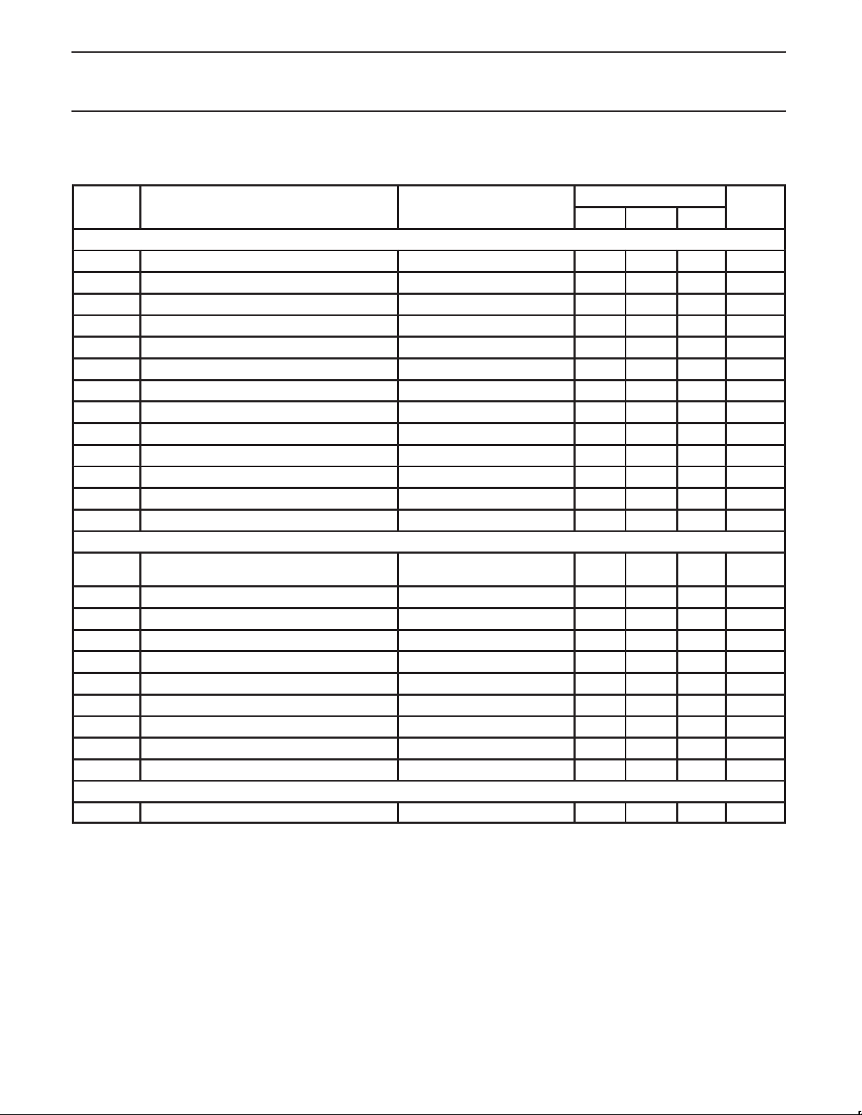
AC ELECTRICAL CHARACTERISTICS
VCC = +3.0V , T
Low Noise Amplifier
f
RF
S
21
S
21
∆S21/∆T Gain temperature sensitivity enabled 0.006 dB/°C
∆S21/∆f Gain frequency variation 800MHz - 1.0GHz ±0.013 dB/MHz
S
12
S
11
S
22
P
-1dB
IP3 Amplifier input third order intercept –7 dBm
NF Amplifier noise figure 1.7 dB
t
ON
t
OFF
Mixer
PG
C
S
11M
NF
M
P
-1dB
IP3
M
IP
2INT
P
RFM-IF
P
LO-IF
P
LO-RFM
P
LO-RF
Overall System
G
SYS
= 25°C; RFIN = 881MHz, f
amb
= 964MHz; unless otherwise stated.
VCO
LIMITS
–3
TYP
+3
RF input frequency range 800 1000 MHz
Amplifier gain 15 dB
Amplifier gain in power-down mode –28 dB
Amplifier reverse isolation @ 881 MHz –28 dB
Amplifier input match With ext. impedance matching –10 dB
Amplifier output match –10 dB
Amplifier input 1dB gain compression –20 dBm
Amplifier turn-on time (Enable Lo → Hi) 120 µs
Amplifier turn-off time (Enable Hi → Lo) 0.3 µs
Mixer power conversion gain: RP = RL = 1.2kΩ
fRF = 881MHz, fLO = 964MHz,
fIF = 83MHz
9.6 dB
Mixer input match Ext. impedance matching req. –10 dB
Mixer SSB noise figure 10 dB
Mixer input 1dB gain compression –14.5 dBm
Mixer input third order intercept 3.3 dBm
Mixer input second order intercept 38 dBm
Mixer RF feedthrough RFIN = –32dBm –45 dBm
LO feedthrough to IF LO = –0dBm –23 dBm
LO to mixer input feedthrough –32 dBm
LO to LNA input feedthrough –42 dBm
System gain LNA + Mixer 23.9 24.6 25.3 dB
1998 Jan 08
4
Philips Semiconductors Product specification
SA6311GHz low voltage LNA and mixer
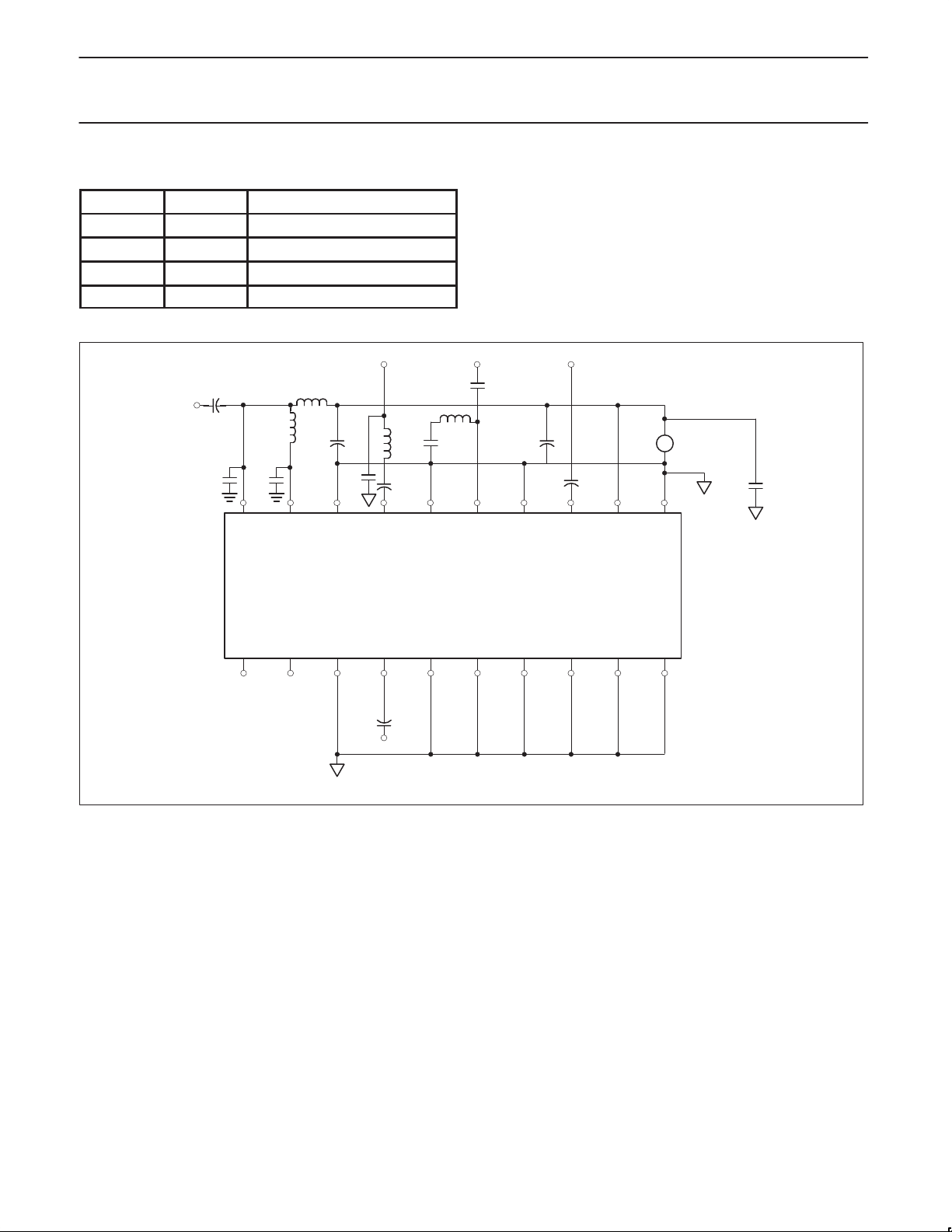
Table 1. Power ON/OFF Control Logic
PD1 PD2
0 0 Full chip power-down
0 1 or open Mixer on, LNA power-down
1 or open 0 Standby (bias on)
1 or open 1 or open Full chip power-on (default)
L3
6.8nH
LNA
IN
C1
100pF
C8
10nF
LNA
OUT
C13
33pF
V
+
CC
–
3V
C9
0.1µF
V
CC
L1
MIXER
OUT
560nH
L4
560n
C2
10nF
C10
2.2pF
MIXER
IN
L6
12nH
C14
6.8pF
C11
10nF
IF
OUT
C3
6.8pF
C16
10pF
C15
10pF
20 19 18 17 16 15 14 13 12 11
MIXER GND GND GND GND
OUT
SA631
PD1 PD2 GND GND GND GND GND GND GND
12345678910
LO
VCO
OUT
OUT
C12
100pF
SR01589
Figure 3. SA631 Application Circuit
1998 Jan 08
5
 Loading...