

Philips sa630 DATASHEETS
RF COMMUNICATIONS PRODUCTS
INPUT/OUTPUT
OUTPUT/INPUT
OUTPUT/INPUT
ENCH1
SA630
Single pole double throw (SPDT) switch
Product Specification
Replaces data of October 10, 1991
IC17 Data Handbook
1997 Nov 07
Philips Semiconductors
Philips Semiconductors Product specification
SA630Single pole double throw (SPDT) switch
DESCRIPTION
The SA630 is a wideband RF switch fabricated in BiCMOS technology and incorporating on-chip CMOS/TTL compatible drivers. Its
primary function is to switch signals in the frequency range DC 1GHz from one 50Ω channel to another. The switch is activated by
a CMOS/TTL compatible signal applied to the enable channel 1 pin
(ENCH1).
The extremely low current consumption makes the SA630 ideal for
portable applications. The excellent isolation and low loss makes
this a suitable replacement for PIN diodes.
The SA630 is available in an 8-pin dual in-line plastic package and
an 8-pin SO (surface mounted miniature) package.
FEA TURES
•Wideband (DC - 1GHz)
•Low through loss (1dB typical at 200MHz)
•Unused input is terminated internally in 50Ω
•Excellent overload capability (1dB gain compression point +18dBm
at 300MHz)
•Low DC power (170µA from 5V supply)
•Fast switching (20ns typical)
•Good isolation (off channel isolation 60dB at 100MHz)
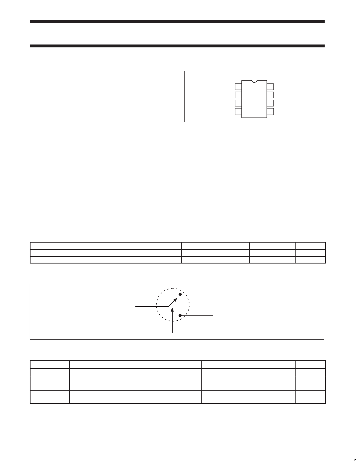
PIN CONFIGURATION
D and N Packages
•Low distortion (IP
1
V
DD
2
GND
3
INPUT
45
ENCH1
Figure 1. Pin Configuration
intercept +33dBm)
3
8
OUT
7
AC GND
6
GND
OUT
•Good 50Ω match (return loss 18dB at 400MHz)
•Full ESD protection
•Bidirectional operation
APPLICA TIONS
•Digital transceiver front-end switch
•Antenna switch
•Filter selection
•Video switch
•FSK transmitter
1
2
SR00578
ORDERING INFORMATION
DESCRIPTION TEMPERATURE RANGE ORDER CODE DWG #
8-Pin Plastic Dual In-Line Package (DIP) -40 to +85°C SA630N SOT97-1
8-Pin Plastic Small Outline (SO) package (Surface-mount) -40 to +85°C SA630D SOT96-1
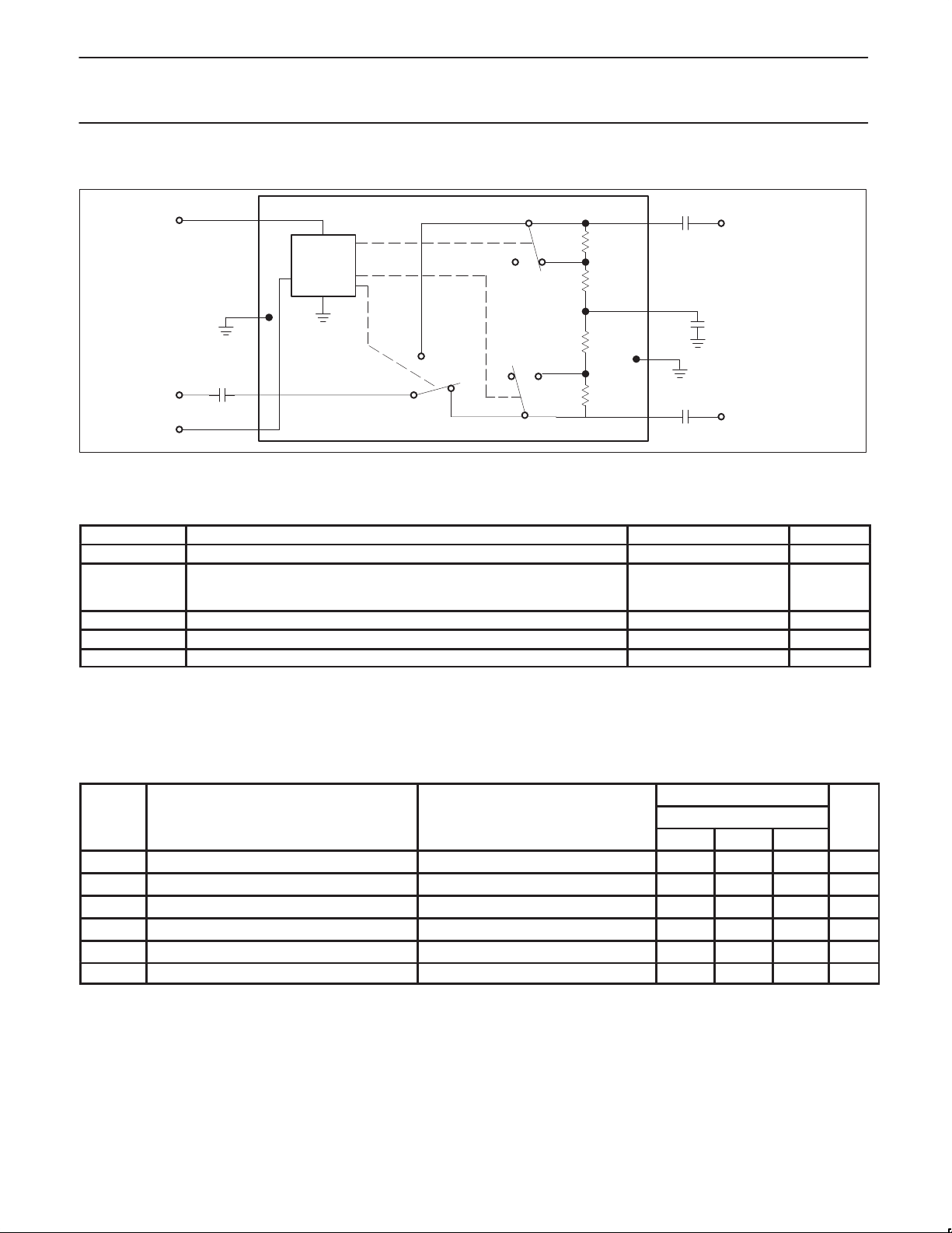
BLOCK DIAGRAM
OUTPUT/INPUT
INPUT/OUTPUT
OUTPUT/INPUT
ENCH1
SR00579
Figure 2. Block Diagram
RECOMMENDED OPERATING CONDITIONS
SYMBOL PARAMETER RATING UNITS
V
DD
T
A
T
J
Supply voltage 3.0 to 5.5V V
Operating ambient temperature range
SA Grade
Operating junction temperature range
SA Grade
-40 to +85 °C
-40 to +105 °C
1997 Nov 07 853-1577 18666
2
Philips Semiconductors Product specification
SA630Single pole double throw (SPDT) switch
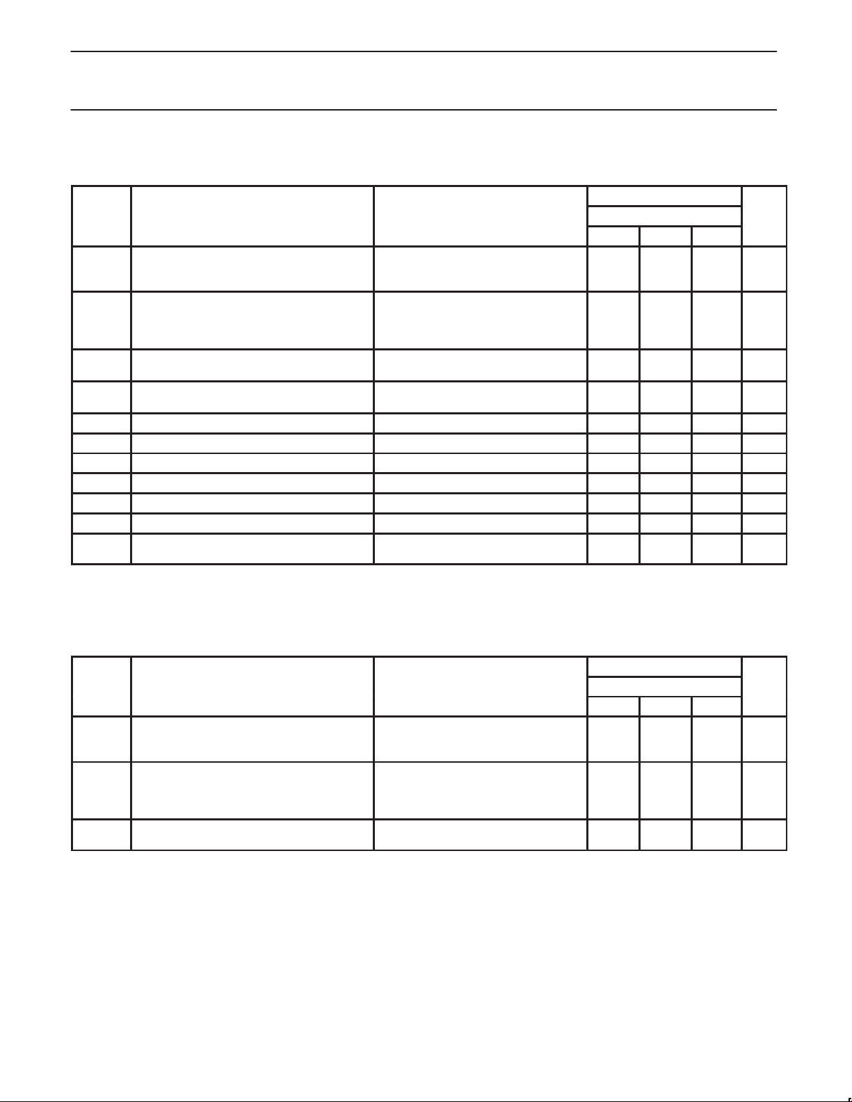
EQUIVALENT CIRCUIT
V
DD
+5V
1
20kΩ
CONTROL
LOGIC
2
50Ω
8
7
OUT
1
AC BYPASS
INPUT
ENCH1
50Ω
3
4
20kΩ
6
OUT
5
2
SR00580
Figure 3. Equivalent Circuit
ABSOLUTE MAXIMUM RATINGS
SYMBOL PARAMETER RATING UNITS
V
T
P
T
DD
P
D
JMAX
MAX
STG
Supply voltage -0.5 to +5.5 V
Power dissipation, TA = 25oC (still air)
8-Pin Plastic DIP
8-Pin Plastic SO
1
1160
780
mW
mW
Maximum operating junction temperature 150 °C
Maximum power input/output +20 dBm
Storage temperature range -65 to +150 °C
NOTES:
1. Maximum dissipation is determined by the operating ambient temperature and the thermal resistance, θ
8-Pin DIP: θ
8-Pin SO: θ
= 108°C/W
JA
= 158°C/W
JA
:
JA
DC ELECTRICAL CHARACTERISTICS
VDD = +5V, TA = 25°C; unless otherwise stated.
LIMITS
SYMBOL PARAMETER TEST CONDITIONS SA630 UNITS
MIN TYP MAX
I
V
V
NOTE:
1. The ENCH1 input must be connected to a valid Logic Level for proper operation of the SA630.
Supply current 40 170 300 µA
DD
V
TTL/CMOS logic threshold voltage
T
Logic 1 level Enable channel 1 2.0 V
IH
Logic 0 level Enable channel 2 -0.3 0.8 V
IL
I
ENCH1 input current ENCH1 = 0.4V -1 0 1 µA
IL
I
ENCH1 input current ENCH1 = 2.4V -1 0 1 µA
IH
1
1.1 1.25 1.4 V
DD
V
1997 Nov 07
3
Philips Semiconductors Product specification
SA630Single pole double throw (SPDT) switch
AC ELECTRICAL CHARACTERISTICS1 - D PACKAGE
VDD = +5V, TA = 25°C; unless otherwise stated.
LIMITS
SYMBOL PARAMETER TEST CONDITIONS SA630 UNITS
MIN TYP MAX
DC - 100MHz
S21, S12Insertion loss (ON channel)
S21, S12Isolation (OFF channel)
S11, S22Return loss (ON channel)
S11, S22Return loss (OFF channel)
t
Switching speed (on-off delay) 50% TTL to 90/10% RF 20 ns
D
tr, t
P
IP
IP
NF Noise figure (ZO = 50Ω )
NOTE:
1. All measurements include the effects of the D package SA630 Evaluation Board (see Figure 4B). Measurement system impedance is 50Ω .
2. The placement of the AC bypass capacitor is critical to achieve these specifications. See the applications section for more details.
Switching speeds (on-off rise/fall time) 90%/10% to 10%/90% RF 5 ns
f
Switching transients 165 mV
1dB gain compression DC - 1GHz +18 dBm
-1dB
Third-order intermodulation intercept 100MHz +33 dBm
3
Second-order intermodulation intercept 100MHz +52 dBm
2
2
500MHz
900MHz
10MHz
100MHz
500MHz
900MHz
DC - 400MHz
900MHz
DC - 400MHz
900MHz
100MHz
900MHz
70
24
1
1.4
2
80
60
50
30
20
12
17
13
1.0
2.0
2.8
dB
dB
dB
dB
P-P
dB
AC ELECTRICAL CHARACTERISTICS1 - N PACKAGE
VDD = +5V, TA = 25°C; all other characteristics similar to the D-Package, unless otherwise stated.
LIMITS
SYMBOL PARAMETER TEST CONDITIONS SA630 UNITS
MIN TYP MAX
DC - 100MHz
S21, S12Insertion loss (ON channel)
S21, S12Isolation (OFF channel)
NF Noise figure (ZO = 50Ω )
NOTE:
1. All measurements include the effects of the N package SA630 Evaluation Board (see Figure 4C). Measurement system impedance is 50Ω .
APPLICATIONS
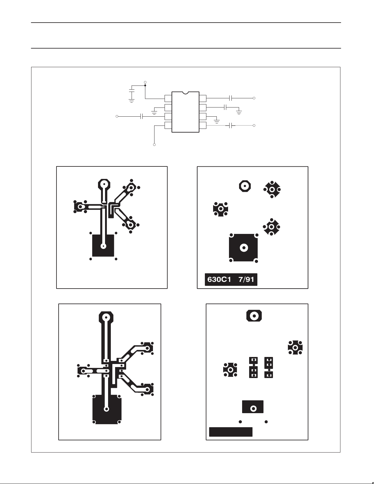
The typical applications schematic and printed circuit board layout of
the SA630 evaluation board is shown in Figure 4. The layout of the
board is simple, but a few cautions need to be observed. The input
and output traces should be 50Ω. The placement of the AC bypass
capacitor is
two channels is desired. The trace from Pin 7 should be drawn back
towards the package and then be routed downwards. The capacitor
extremely critical
if a symmetric isolation between the
500MHz
900MHz
10MHz
100MHz
500MHz
900MHz
100MHz
900MHz
should be placed straight down as close to the device as practical.
For better isolation between the two channels at higher frequencies,
it is also advisable to run the two output/input traces at an angle.
This also minimizes any inductive coupling between the two traces.
The power supply bypass capacitor should be placed close to the
device. Figure 10 shows the frequency response of the SA630.
The loss matching between the two channels is excellent to 1.2GHz
as shown in Figure 13.
58
1
1.4
2.5
68
50
37
15
1.0
2.5
dB
dB
dB
1997 Nov 07
4
Philips Semiconductors Product specification
SA630Single pole double throw (SPDT) switch
V
DD
+5V
0.1µF
INPUT
0.01µF
a. Evaluation Board Schematic
D and N Packages
1
GND
2
3
45
ENCH
1
8
7
6
AC GND
GND
0.01µF
0.01µF
0.01µF
OUT
OUT
1
2
1997 Nov 07
b. 630 D-Package Board Layout
630N1 7/91
c. 630 N-Package Board Layout
Figure 4. Board and Package Graphics
5
SR00581
 Loading...