

Philips sa626 DATASHEETS

INTEGRATED CIRCUITS
SA626
Low voltage high performance mixer FM
IF system with high-speed RSSI
Product specification
IC17 Data Handbook
1997 Sept 25
Philips Semiconductors Product specification
Low voltage high performance mixer FM IF
system with high-speed RSSI
DESCRIPTION
The SA626 is a low-voltage high performance monolithic FM IF
system incorporating a mixer/oscillator, two limiting intermediate
frequency amplifiers, quadrature detector, high speed logarithmic
received signal strength indicator (RSSI), voltage regulator and
audio and fast RSSI op amps. The SA626 is available in 20-lead
SOL (surface-mounted small outline large package) and 20-lead
SSOP (shrink small outline package).
The SA626 was designed for high bandwidth portable
communication applications and will function down to 2.7V . The RF
section is similar to the famous NE605. The audio and RSSI
outputs have amplifiers. The RSSI output has access to the
feedback pin. This enables the designer to level adjust the outputs
or add filtering.
SA626 incorporates a power down mode which powers down the
device when Pin 8 is low. Power down logic levels are CMOS and
TTL compatible with high input impedance.
APPLICATIONS
•Digital cordless telephones
•Digital cellular telephones
•Digital cellular base stations
•Portable high performance communications receivers
•Single conversion VHF/UHF receivers
•SCA receivers
•RF level meter
•Spectrum analyzer
•Instrumentation
•FSK and ASK data receivers
•Log amps
•Wideband low current amplification
FEA TURES
•Fast RSSI rise and fall times
•Low power consumption: 6.5mA typ at 3V
•Power down mode (I
= 200µA)
CC
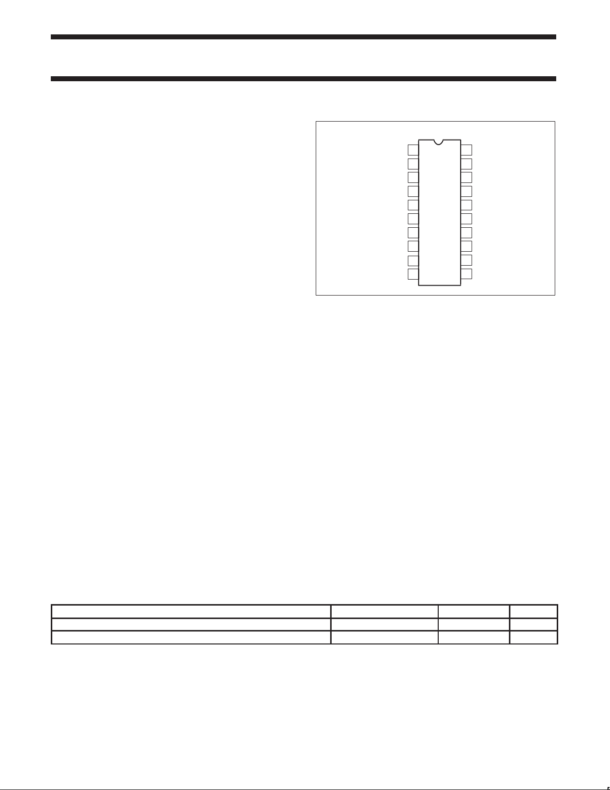
PIN CONFIGURATION
•Mixer input to >500MHz
•Mixer conversion power gain of 11dB at 240MHz
•Mixer noise figure of 14dB at 240MHz
•XTAL oscillator effective to 150MHz (L.C. oscillator to 1GHz, local
•92dB of IF Amp/Limiter power gain
•25MHz limiter small signal bandwidth
•Temperature compensated logarithmic Received Signal Strength
•Audio output internal buffer
•RSSI output internal buffer
•Internal op amps with rail-to-rail outputs
•10.7MHz filter matching (330Ω) reduces external component
•Excellent sensitivity: 0.54µV into 50Ω matching network for 12dB
•SA626 meets cellular radio specifications
•ESD hardened
SA626
D and DK Packages
RF
1
IN
RF BYPASS 2
XTAL OSC EMITTER 3
XTAL OSC (BASE) 4
V
5
CC
RSSI FEEDBACK
RSSI
POWER DOWN CONTROL
AUDIO OUT
QUADRATURE IN
oscillator can be injected)
Indicator (RSSI) with a dynamic range in excess of 90dB
count; suitable for crystal/ceramic/LC filters
SINAD (Signal to Noise and Distortion ratio) for 1kHz tone with RF
at 240MHz and IF at 10.7MHz
6
7
OUT
8
9
10
Figure 1. Pin Configuration
20 MIXER OUT
19
IF AMP DECOUPLING
18 IF AMP IN
17
IF AMP DECOUPLING
16 IF AMP OUT
15 GND
14 LIMITER IN
LIMITER DECOUPLING
13
12
LIMITER DECOUPLING
11 LIMITER OUT
SR00470
ORDERING INFORMATION
DESCRIPTION TEMPERATURE RANGE ORDER CODE DWG #
20-Pin Plastic Small Outline Large (SOL) package (Surface-mount) -40 to +85°C SA626D SOT163-1
20-Pin Plastic Shrink Small Outline Package (Surface-mount) -40 to +85°C SA626DK
1997 Sept 25 853-1723 18427
2
SOT266-1
Philips Semiconductors Product specification
Low voltage high performance mixer FM IF system
with high-speed RSSI
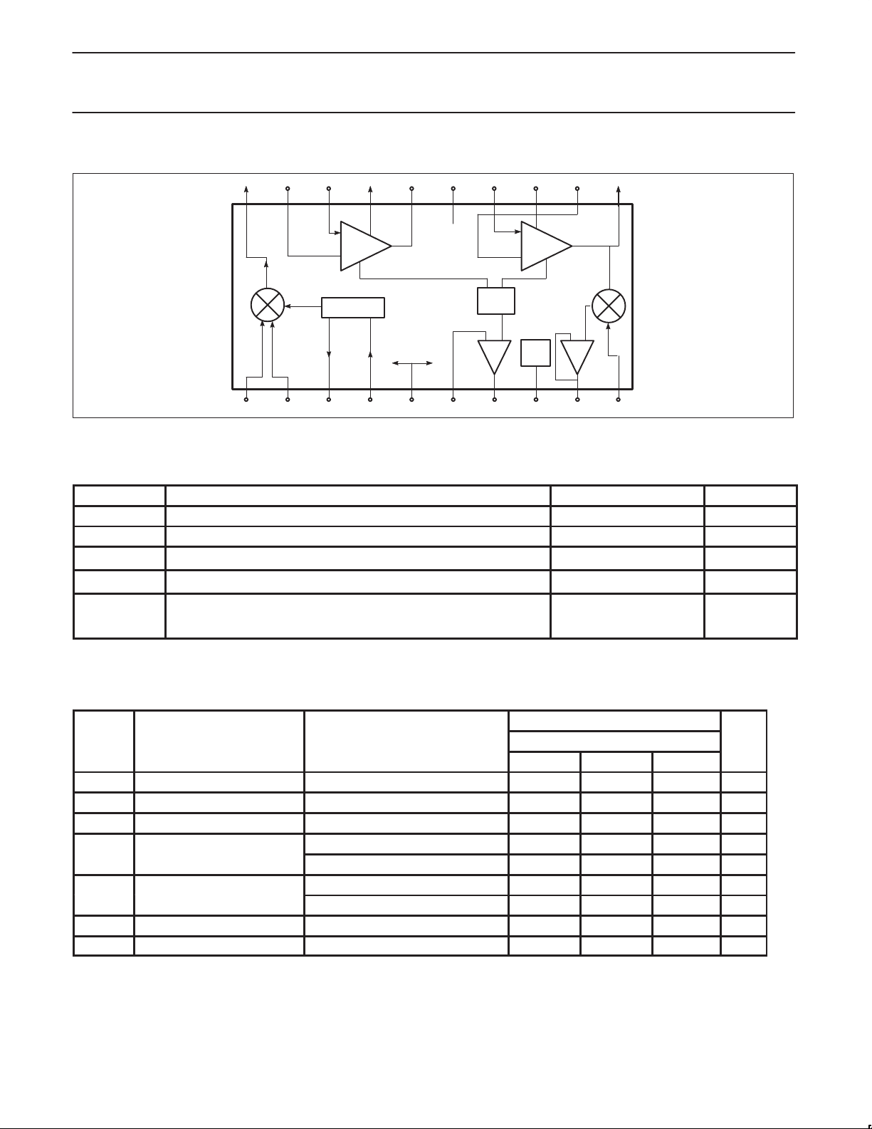
BLOCK DIAGRAM
20 19 18 17 16 15 14 13 12 11
IF
AMP
MIXER
OSCILLATOR
EB
Figure 2. Block Diagram
ABSOLUTE MAXIMUM RATINGS
SYMBOL PARAMETER RATING UNITS
T
V
V
θ
CC
IN
STG
T
A
JA
Single supply voltage 0.3 to 7 V
Voltage applied to any other pin –0.3 to (VCC+0.3) V
Storage temperature range -65 to +150
Operating ambient temperature range SA626 –40 to +85
Thermal impedance D package 90
DK package 117
GND
V
CC
RSSI
FAST
RSSI
LIMITER
QUAD
+–
PWR
DWN
+–
AUDIO
10987654321
SA626
SR00471
°C
°C
°C/W
°C/W
DC ELECTRICAL CHARACTERISTICS
VCC = +3V, TA = 25°C; unless otherwise stated.
LIMITS
SYMBOL PARAMETER TEST CONDITIONS SA626 UNITS
MIN TYP MAX
V
I
I
t
t
OFF
Power supply voltage range 2.7 3.0 5.5 V
CC
DC current drain Pin 8 = HIGH 5.5 6.5 7.5 mA
CC
Standby Pin 8 = LOW 0.2 0.5 mA
CC
Input current Pin 8 LOW –10 10 µA
Pin 8 HIGH –10 10 µA
Input level Pin 8 LOW 0 0.3V
Pin 8 HIGH 0.7V
Power up time RSSI valid (10% to 90%) 10 µs
ON
CC
Power down time RSSI invalid (90% to 10%) 5 µs
CC
V
CC
V
V
1997 Sept 25
3
Philips Semiconductors Product specification
Low voltage high performance mixer FM IF system
with high-speed RSSI
AC ELECTRICAL CHARACTERISTICS
TA = 25°C; VCC = +3V, unless otherwise stated. RF frequency = 240.05MHz + 14.5dBV RF input step-up; IF frequency = 10.7MHz; RF level =
-68dBm; FM modulation = 1kHz with ±125kHz peak deviation. Audio output with C-message weighted filter and de-emphasis filter. Test circuit
Figure 1. The parameters listed below are tested using automatic test equipment to assure consistent electrical characteristics. The limits do
not represent the ultimate performance limits of the device. Use of an optimized RF layout will improve many of the listed parameters.
LIMITS
SYMBOL PARAMETER TEST CONDITIONS SA626 UNITS
MIN TYP MAX
Mixer/Osc section (ext LO = 160mV
f
Input signal frequency 500 MHz
IN
f
OSC
IF section
THD Total harmonic distortion -43 –38 dB
S/N Signal-to-noise ratio No modulation for noise 60 dB
RF/IF section (int LO)
External oscillator (buffer) 500 MHz
Noise figure at 240MHz 14 dB
Third-order input intercept point Matched f1=240.05; f2=240.35MHz -16 dBm
Conversion power gain Matched 14.5dBV step-up 8 11 14 dB
RF input resistance Single-ended input 700 Ω
RF input capacitance 3.5 pF
Mixer output resistance (Pin 20) 330 Ω
IF amp power gain 38 dB
Limiter amp power gain 54 dB
Input limiting -3dB Test at Pin 18 –105 dBm
AM rejection 80% AM 1kHz 50 dB
Audio level Unity gain 120 160 200 mV
Audio DC level Pin 9, no signal 1.0 V
SINAD sensitivity IF level = -111dBm 16 dB
IF RSSI output with buffer IF level = -118dBm 0.2 0.5 V
IF RSSI output rise time IF frequency = 10.7MHz
(10kHz pulse, no 10.7MHz filter) RF level = -56dBm 1.2 µs
(no RSSI bypass capacitor) RF level = -28dBm 1.1 µs
IF RSSI output fall time IF frequency = 10.7MHz
(10kHz pulse, no 10.7MHz filter) RF level = -56dBm 2.0 µs
(no RSSI bypass capacitor) RF level = -28dBm 7.3 µs
RSSI range 90 dB
RSSI accuracy +1.5 dB
IF input impedance 330 Ω
IF output impedance 330 Ω
Limiter input impedance 330 Ω
Limiter output impedance 300 Ω
Limiter output level with no load 130 mV
Audio level RF level = -10dBm 160 mV
System RSSI output RF level = -10dBm 1.4 V
System SINAD RF level = -106dBm 12 dB
RMS
)
IF level = -68dBm 0.3 0.6 1.0 V
IF level = -10dBm 0.9 1.3 1.8 V
SA626
RMS
RMS
RMS
1997 Sept 25
4
Philips Semiconductors Product specification
Low voltage high performance mixer FM IF system
with high-speed RSSI
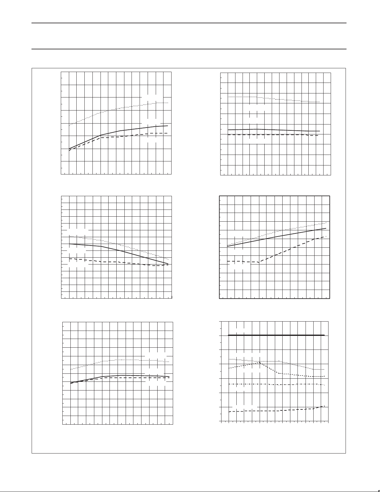
9.0
8.5
V
8.0
7.5
7.0
6.5
SUPPLY CURRENT (mA)
6.0
5.5
5.0
–50 –40 –30 –20 –10 0 10 20 30 40 50 60 70 80 90
TEMPERATURE (°C)
= 5V
CC
VCC = 3V
= 2.7V
V
CC
Supply Current vs Temp and Supply Voltage Power Down Supply Current vs Temp and Supply Voltage
20
19
18
17
16
15
14
13
12
MIXER GAIN (dB)
11
10
9
8
7
6
5
Mixer Power Gain vs Temperature and Supply Voltage
300
275
250
225
200
175
150
AUDIO (mV)
125
100
75
50
25
= 5V
V
CC
VCC = 3V
= 2.7V
V
CC
–50 –40 –30 –20 –10 0 10 20 30 40 50 60 70 80 90
0
–50 –40 –30 –20 –10 0 10 20 30 40 50 60 70 80 90
TEMPERATURE (°C)
TEMPERATURE (°C)
= 5V
V
CC
VCC = 3V
= 2.7V
V
CC
Third Order Input Intercept Point vs Temp and Supply Voltage
Audio Output Level vs. Temp and Supply Voltage
Figure 3. Performance Characteristics
0.50
0.45
0.40
0.35
0.30
0.25
0.20
0.15
0.10
POWER DOWN SUPPLY CURRENT (mA)
0.05
0.00
–50 –40 –30 –20 –10 0 10 20 30 40 50 60 70 80 90
–6
–8
–10
–12
–14
–16
–18
–20
–22
–24
–26
THIRD ORDER INPUT INTERCEPT POINT dBm)
–28
–30
–50 –40 –30 –20 –10 0 10 20 30 40 50 60 70 80 90
20
0
–20
–40
AUDIO (dB)
–60
–80
–100
–120
–50–40 –30 –20 –10 0 10 20 30 40 50 60 70 80 90
12dB SINAD and Relative Audio, THD, Noise and AM
Rejection for VCC = 3V vs Temperature RF = 240MHz,
Level = –68dBm, Deviation = 125kHz
= 5V
V
CC
V
= 3V
CC
VCC = 2.7V
V
= 5V
CC
VCC = 3V
= 2.7V
V
CC
AUDIO
AM REJECTION
DISTORTION
NOISE
12dB SINAD
SA626
100
TEMPERATURE (°C)
TEMPERATURE (°C)
TEMPERATURE (°C)
SR00472
1997 Sept 25
5
 Loading...