

Philips sa621 DATASHEETS

INTEGRATED CIRCUITS
SA621
1GHz - Low voltage LNA, mixer and VCO
Product specification 1997 Nov 07
IC17 Data handbook
Philips Semiconductors Product specification
SA6211GHz low voltage LNA, mixer and VCO
DESCRIPTION
The SA621 is a combined low-noise amplifier, mixer and VCO
designed for high-performance low-power communication systems
from 800-1000MHz. The low-noise preamplifier has a 1.7dB noise
figure at 881MHz with 15dB gain and an IP3 intercept of -7dBm at
the input. The gain is stabilized by on-chip compensation to vary
less than ±0.2dB over -40 to +85°C temperature range. The
wide-dynamic-range mixer has a 12dB noise figure and IP3 of
+4.5dBm at the input at 881MHz. The integrated VCO circuit with
external resonator produces a high quality LO signal that drives the
mixer and is buffered to an external PLL synthesizer IC. The
nominal current drawn from a single 3V supply is 13.3mA.
Additionally, the entire circuit can be powered down to further reduce
the supply current to less than 20µA.
FEATURES
•Low current consumption
•Outstanding gain and noise figure
•Excellent gain stability versus temperature and supply voltage
•LNA, mixer and VCO power down capability
•Monotonic VCO frequency vs control voltage
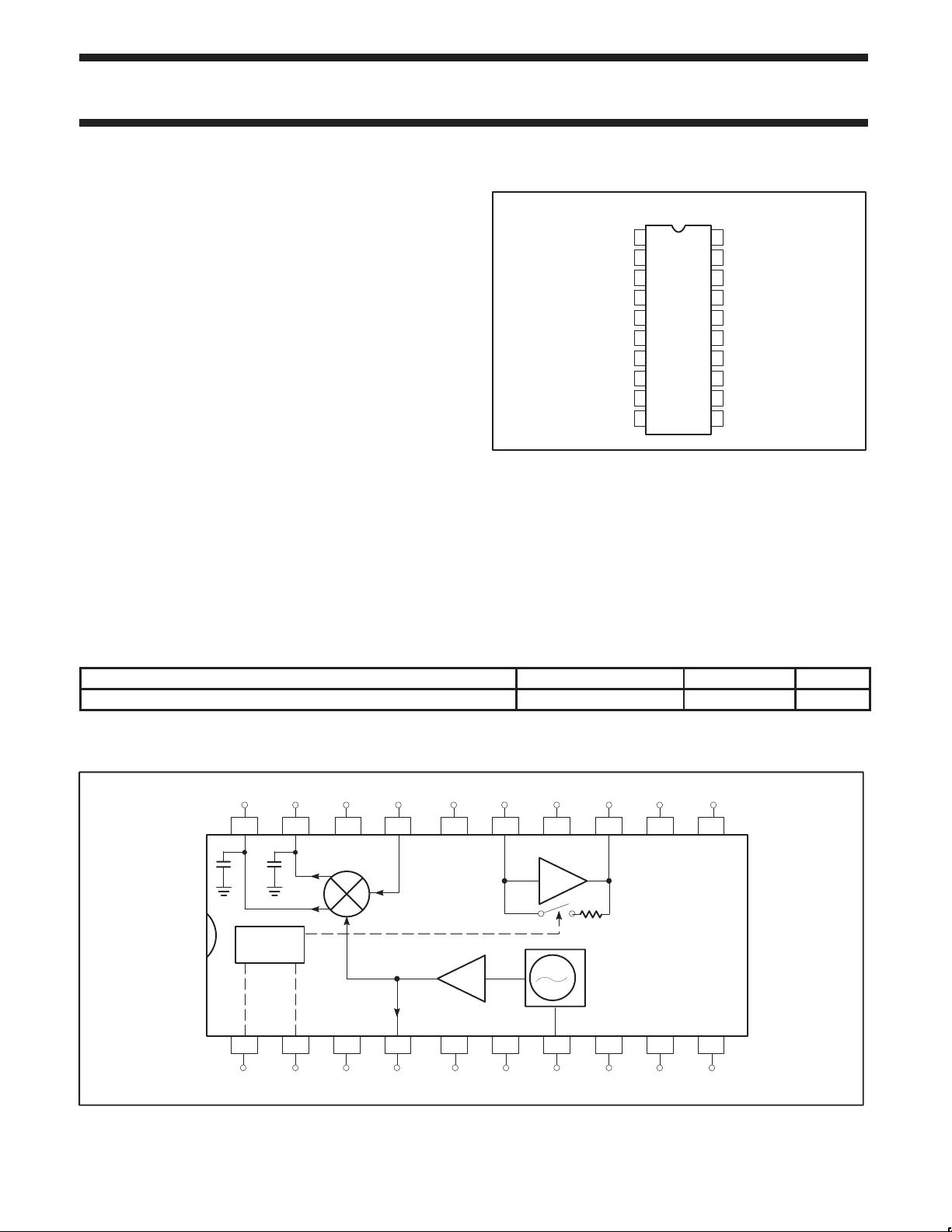
PIN CONFIGURATION
1
PD1
2
PD2
3
GND
4
LO OUT
5
GND
GND
6
7
TANK
8
GND
GND
9
BYPASS
10
Figure 1. Pin Configuration
APPLICATIONS
•900MHz cellular and cordless front-end
•Spread spectrum receivers
•RF data links
•UHF frequency conversion
•Portable radio
20
MIXER OUT
MIXER OUT
19
18
GND
17
MIXER IN
GND
16
LNA IN
15
GND
14
LNA OUT
13
12
V
CC
GND
11
SR01429
ORDERING INFORMATION
DESCRIPTION TEMPERATURE RANGE ORDER CODE DWG #
20-Pin Thin Shrink Small Outline Package (Surface-mount, TSSOP)
BLOCK DIAGRAM
OUT
MIXER
OUT
GND
MIXER
20 19 18 17 16
10pF 10pF
PD1 PD2 GND
MIXER
IN
43215
LO GND BYPASS
OUT
Figure 2. SA621 Block Diagram
GND
GND
-40 to +85°C
LNA
IN GND
GND
LNA
OUT
V
CC
15 14 13 12 11
LNA
761098
GND GND
TANK
SA621DH SOT360-1
SR01428
1997 Nov 07 853-1849 018660
2
Philips Semiconductors Product specification
SYMBOL
PARAMETER
TEST CONDITIONS
UNITS
ICCSu ly current
SA6211GHz low voltage LNA, mixer and VCO
ABSOLUTE MAXIMUM RATINGS
SYMBOL PARAMETER RATING UNITS
V
T
P
T
CC
V
IN
P
D
JMAX
MAX
STG
Supply voltage
Voltage applied to any other pin -0.3 to (VCC + 0.3) V
Power dissipation, TA = 25°C (still air)2
Maximum operating junction temperature 150 °C
Maximum power input/output +20 dBm
Storage temperature range –65 to +150 °C
NOTE:
1. Transients exceeding 8V on V
2. Maximum dissipation is determined by the operating ambient temperature and the thermal resistance,
θ
3. Pins 19 and 20 are ESD sensitive (mixer outputs).
JA
RECOMMENDED OPERATING CONDITIONS
SYMBOL PARAMETER RATING UNITS
V
CC
T
A
T
J
Supply voltage 2.7 to 5.5 V
Operating ambient temperature range -40 to +85 °C
Operating junction temperature -40 to +105 °C
1
20-Pin Plastic SSOP
pin may damage product.
CC
: 20-Pin SSOP = 110°C/W
-0.3 to +6 V
980 mW
DC ELECTRICAL CHARACTERISTICS
VCC = +3.0V , TA = 25°C; unless otherwise stated.
pp
V
PD logic threshold voltage 1.2 1.6 1.8 V
T
V
V
Logic 1 level 2.0 V
IH
Logic 0 level –0.3 0.8 V
IL
I
PD1 input current Enable = 0.4V 10 µA
IL
I
PD2 input current Enable = 2.4V 10 µA
IH
LIMITS
MIN TYP MAX
Full power-on 13.3 mA
LNA powered-down 10 mA
Standby (VCO + bias) 5.7 mA
Full power-down 20 µA
CC
V
1997 Nov 07
3
Philips Semiconductors Product specification
SYMBOL
PARAMETER
TEST CONDITIONS
UNITS
2
VCO hase noise
2
dBc/Hz
SA6211GHz low voltage LNA, mixer and VCO
AC ELECTRICAL CHARACTERISTICS
VCC = +3.0V , TA = 25°C; RFIN = 881MHz, f
Low Noise Amplifier
f
S
S
RF input frequency range 800 1000 MHz
RF
Amplifier gain 15 dB
21
Amplifier gain in power-down mode -28 dB
21
∆S21/∆T Gain temperature sensitivity enabled 0.006 dB/°C
∆S21/∆f Gain frequency variation 800MHz - 1.0GHz ±0.013 dB/MHz
S
S
S
P
Amplifier reverse isolation @ 881 MHz -28 dB
12
Amplifier input match With ext. impedance matching -10 dB
11
Amplifier output match -10 dB
22
Amplifier input 1dB gain compression -20 dBm
-1dB
IP3 Amplifier input third order intercept -7 dBm
NF Amplifier noise figure 1.7 dB
t
t
OFF
Amplifier turn-on time (Enable Lo → Hi) 120 µs
ON
Amplifier turn-off time (Enable Hi → Lo) 0.3 µs
Mixer
PG
S
NF
P
IP3
IP
P
RFM-IF
P
LO-IF
P
LO-RFM
P
LO-RF
Voltage Controlled Oscillator (VCO)
f
VCO
P
Mixer power conversion gain: RP = RL = 1.2kΩ,
C
Mixer input match Ext. impedance matching req. -10 dB
11M
Mixer SSB noise figure 12 dB
M
Mixer input 1dB gain compression -10 dBm
-1dB
Mixer input third order intercept 4.5 dBm
M
Mixer input second order intercept 15 dBm
2INT
Mixer RF feedthrough RFIN = -25dBm -41 dBm
LO feedthrough to IF LO = -10dBm -23 dBm
LO to mixer input feedthrough -52 dBm
LO to LNA input feedthrough -38 dBm
1
VCO frequency range 883 1083 MHz
VCO power out See Figure 3 -10 -8 dBm
VCO
p
Harmonic content -22 dBc
Residual modulation 45 dB
Pulling figure VSWR=2:1, all phases ±500 kHz
Pushing figure ±100 kHz/V
Overall System
G
System gain LNA + Mixer 23.0 23.7 24.4 dB
SYS
NOTES:
1. VCO performance dependent on external components.
2. Based on copper-plated 2mm ceramic resonator (1/4 wave), f = 1025MHz, and can be improved by silver-plated or larger resonators.
= 964MHz; unless otherwise stated.
VCO
fRF = 881MHz, fLO = 964MHz,
Offset = 30kHz -109
Offset = 60kHz -115
= 83MHz
f
IF
–3
LIMITS
TYP
+3
8.7 dB
1997 Nov 07
4
Philips Semiconductors Product specification
SA6211GHz low voltage LNA, mixer and VCO
Table 1. Power ON/OFF Control Logic
PD1 PD2
0 0 Full chip power-down
0 1 or open VCO on, Mixer on, LNA power-down
1 or open 0 VCO on, LNA and Mixer power-down
1 or open 1 or open Full chip power-on (default)
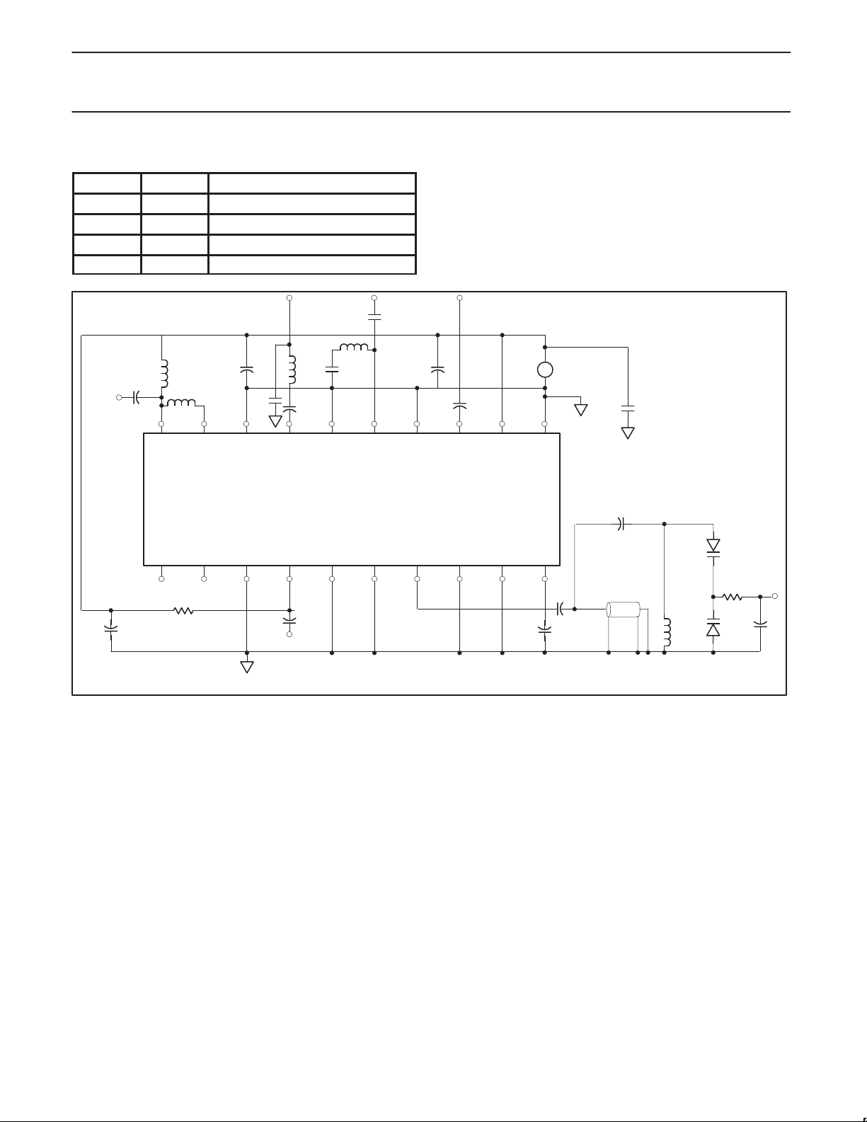
C1
100pF
L6
12nH
L3
C3
6.8pF
IF
OUT
L1
560nH
L4
560nH
20 19 18 17 16 15 14 13 12 11
OUT
MIXER
OUT
MIXER GND GND GND GND
C2
10nF
C10
2.2pF
MIXER
IN
C14
6.8pF
C11
10nF
6.8nH
LNA
IN
C8
10nF
LNA
OUT
C13
33pF
V
+
CC
–
3V
C9
0.1µF
V
CC
SA621
PD1 PD2 GND GND GND TANK GND GND BYPASS
12345678910
R2
C6
10nF
24Ω
LO
VCO
OUT
OUT
C12
100pF
Figure 3. SA621 Applications Circuit
C10
220pF
C5
.5pF
C4
2.2pF
MURATA 2mm
1/4 WAVE
FREQ=1025MHz
L7
18.5nH
Hi–Q
VCO
CONTROL
D1
R1
D7
5.1kΩ
10nF
SR01424
1997 Nov 07
5
 Loading...