

Philips SA5778 Datasheet
INTEGRATED CIRCUITS
SA5778
Serial triple gauge driver (STGD)
Product specification
Supersedes data of 1997 May 27
IC18 Data Handbook
1998 Apr 03
Philips Semiconductors Product specification
SA5778Serial triple gauge driver (STGD)
DESCRIPTION
The Serial Triple Gauge Driver (STGD), is a single chip air core
driver providing drive to one major gauge, and two minor gauges, for
automotive applications such as Speedometer, Fuel, Temperature,
Tachometer, Volts, and Oil pressure information display. The STGD
operates in conjunction with a microcontroller receiving serial data
inputs, and can provide status back to the microcontroller either
serially or via a status line. The protocol is compatible with the
Philips Single Gauge Driver (SGD) and Dual Gauge Driver (DGD).
The STGD also includes a protected battery supply for external
single Serial Gauge Drivers or Dual Gauge Drivers.
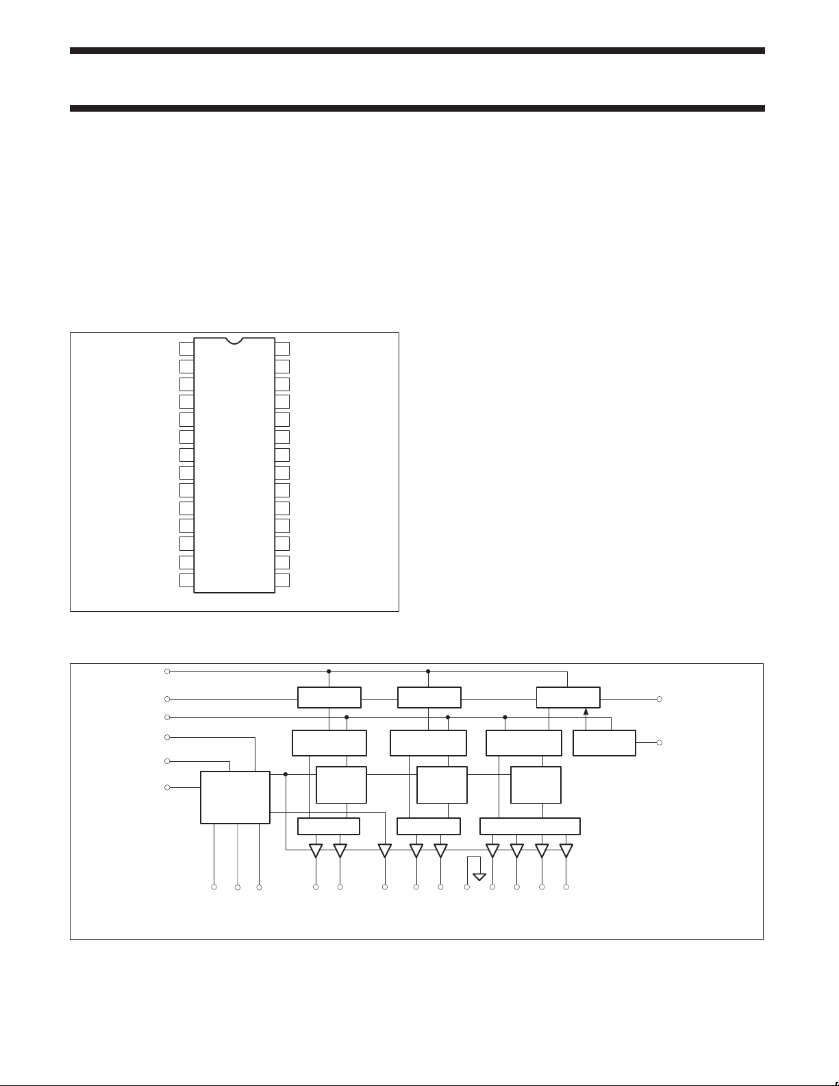
PIN CONFIGURATION
SIN+
1
RUN
2
GOE
3
SwCONTROL
SwBATT1
SwBATT2
DATA
4
5
GND GND
6
GND
7
GND GND
821
GND GND
9
V
10
BATT
11
12
OUT
COM
13
C2–
14
SIN–
28
COS+
27
26
COS–
ST
25
24
S
CLK
23
GND
22
20
CS
19
DATA
18
IN
C1–
17
C1+
16
C2+
15
FEATURES
•Major Gauge 10-bit resolution Drive provides 0.35° resolution
– Sine/Cosine outputs for 360° operation
– 0.2° accuracy typical throughout entire range
•Minor gauge drivers provide 0.35° resolution
– 112° operation
– 0.5° accuracy typical throughout entire range
•Serial Data Input
– Supports interface from microcontrollers
– Compatible with Philips SGD SA5775A and DGD SA5777A
•Serial Data Output
– Permits the STGD to be wired in series using a common chip
select to additional STGDs, SGDs, and DGDs
– Permits fault status information to be returned to the
microcontroller
•Over Voltage Protection, Over Temperature Protection and Low
Standby Current Operation
– Gauge drivers disabled when supply voltage exceeds specified
operating voltage, protection to 40V .
– Gauge drivers disabled when die temperature exceeds
operating range
– External switch may supply overvoltage protected battery
supply to other devices operating off battery
•Thermally Enhanced SO-28 surface mount package
Figure 1. Pin Configuration
BLOCK DIAGRAM
S
CLK
DATA
IN
CS
GOE
RUN
V
BATT
BIAS, TSD
SwBATT,
COMMON
REFERENCE
SwBATT1
SwControl
SR01116
MINOR GAUGE 2
10-BIT SR 10-BIT SR 10-BIT SR
9-BIT DATA
ENABLE
SwBATT2
MINOR GAUGE 1 MAJOR GAUGE
LATCH
7-BIT
MUX
C2–
Tan
DAC
C2+
9-BIT DATA
LATCH
7-BIT
Tan
DAC
MUX MUX
C1–
COM
C1+
GND
10-BIT DATA
LATCH
COS–
Figure 2. STGD Internal Block Diagram
7–BIT, SINE
/COSINE
DAC
SIN–
COS+
4-BIT STATUS
LATCH
SIN+
DATA
ST
OUT
SR01117
1998 Apr 03 853–2055 19199
2
Philips Semiconductors Product specification
Á
Á
Á
Á
Á
Á
Á
Á
Á
Á
Á
Á
Á
Á
Á
Á
Á
Á
Á
Á
Á
Á
Á
Á
Á
Á
Á
Á
Á
Á
SA5778Serial triple gauge driver (STGD)
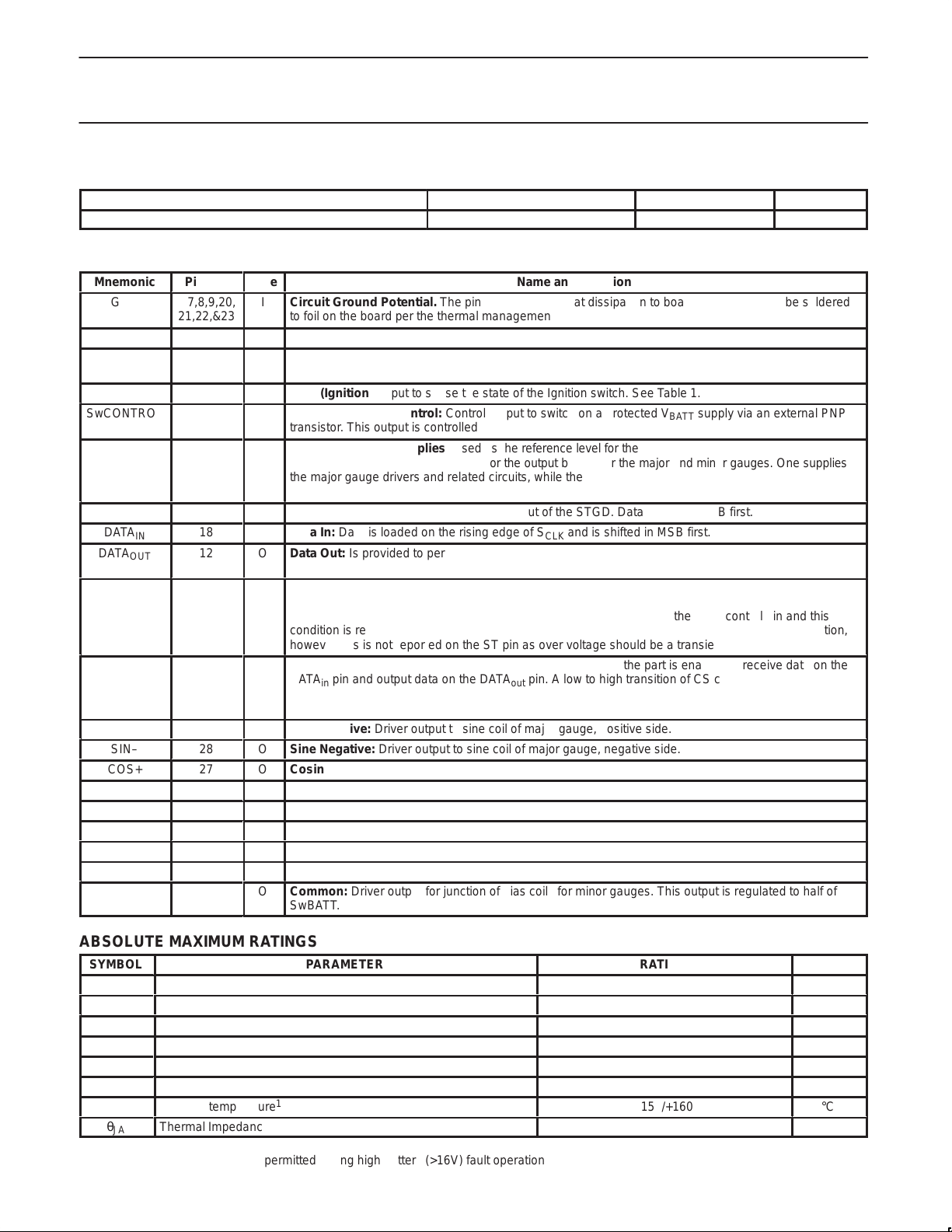
ORDERING INFORMATION
DESCRIPTION TEMPERATURE RANGE ORDER CODE DWG #
28-Pin Small Outline (SO) thermally enhanced Package –40 to +105°C SA5778D SOT136-1
PIN DESCRIPTION
Mnemonic
GND
V
BATT
GOE
ÁÁÁ
RUN
SwCONTROL
ÁÁÁ
SwBATT1
SwBATT2
ÁÁÁ
ÁÁÁ
S
CLK
DATA
IN
DATA
OUT
ÁÁÁ
ST
ÁÁÁ
ÁÁÁ
CS
ÁÁÁ
ÁÁÁ
SIN+
SIN–
COS+
COS–
C1+
C1–
C2+
C2–
COM
ÁÁÁ
Pin No.
6,7,8,9,20,
21,22,&23
10
3
ÁÁ
2
4
ÁÁ
5,
11
ÁÁ
ÁÁ
24
18
12
ÁÁ
25
ÁÁ
ÁÁ
19
ÁÁ
ÁÁ
1
28
27
26
16
17
15
14
13
ÁÁ
Type
I
Circuit Ground Potential. The pins are used for heat dissipation to board. All pins should be soldered
Name and Function
to foil on the board per the thermal management description.
I
Battery supply voltage
I
Gauge Output Enable: A high on this input enables normal operation of the gauge coil drivers.
See Table 1.
ББББББББББББББББББББББББ
I
RUN (Ignition): Input to sense the state of the Ignition switch. See Table 1.
O
Switched Battery Control: Control output to switch on a protected V
ББББББББББББББББББББББББ
transistor. This output is controlled by the RUN input, GOE input and the on chip protection circuits.
I
Switched Battery Supplies: Used as the reference level for the DACs, bias voltage for the second coils
I
of the minor gauges, and the supply for the output buffers for the major and minor gauges. One supplies
ББББББББББББББББББББББББ
the major gauge drivers and related circuits, while the other supplies the minor gauge circuits. Both
SwBATT inputs must be connected to the control transistor as the two inputs are not connected internally.
ББББББББББББББББББББББББ
I
Serial Clock: Used to clock data into and out of the STGD. Data is shifted MSB first.
I
Data In: Data is loaded on the rising edge of S
O
Data Out: Is provided to permit the STGD to pass status information back to the controlling
microcontroller, and to allow multiple devices to be connected in series.
ББББББББББББББББББББББББ
O
Status Output: This is an open drain output. Status outputs from several devices may be wire OR’ed
and is shifted in MSB first.
CLK
supply via an external PNP
BATT
together. This output is low when the outputs are disabled due to a fault condition. The outputs may be
disabled due to shorted outputs, over temperature, power up reset, or the GOE control pin and this
ББББББББББББББББББББББББ
condition is reflected on the ST pin. The outputs will also be disabled due to an over voltage condition,
ББББББББББББББББББББББББ
however this is not reported on the ST pin as over voltage should be a transient condition.
I
Chip Select: Active high chip select input. When CS is high, the part is enabled to receive data on the
pin and output data on the DATA
DATA
in
ББББББББББББББББББББББББ
the shift register for output. A high to low transition of CS loads gauge data from the shift register into
the data latches.
ББББББББББББББББББББББББ
O
Sine Positive: Driver output to sine coil of major gauge, positive side.
O
Sine Negative: Driver output to sine coil of major gauge, negative side.
O
Cosine Positive: Driver output to cosine coil of major gauge, positive side.
O
Cosine Negative: Driver output to cosine coil of major gauge, negative side.
O
Coil 1 Positive: Driver output to driven coil of minor gauge 1, positive side.
O
Coil 1 Negative: Driver output to driven coil of minor gauge 1, negative side.
O
Coil 2 Positive: Driver output to driven coil of minor gauge 2, positive side.
O
Coil 2 Negative: Driver output to driven coil of minor gauge 2, negative side.
O
Common: Driver output for junction of bias coils for minor gauges. This output is regulated to half of
ББББББББББББББББББББББББ
SwBATT.
pin. A low to high transition of CS captures device status in
out
ABSOLUTE MAXIMUM RATINGS
SYMBOL
V
VIN1
VIN2
VIN3
T
BATT
P
amb
T
θ
Battery supply voltage, with recommended 1K series resistor
Input voltage; Data In, CS, SCLK, GOE
Input voltage; Sw
BATT
Input voltage; RUN, with recommended RC Circuit
Power Dissipation (T
D
Ambient operating temperature
Junction temperature
J
Thermal Impedance
JA
NOTE:
1. 160°C junction temperature is permitted during high battery (>16V) fault operation
1998 Apr 03
PARAMETER
= 105°C) SO-28 Package
amb
1
3
RATING
40
–1 to +7
–1 to +24
–1 to +40
1400
–40 to +105
+150/+160
See Thermal Management Section
UNIT
V
V
V
V
mw
°C
°C
°C/W
Philips Semiconductors Product specification
SYMBOL
PARAMETER
TEST CONDITION
UNITS
Á
Á
Á
Á
Á
Á
Á
Á
Á
Á
Á
Á
Á
Á
Á
Á
SYMBOL
PARAMETER
TEST CONDITION
UNITS
SA5778Serial triple gauge driver (STGD)
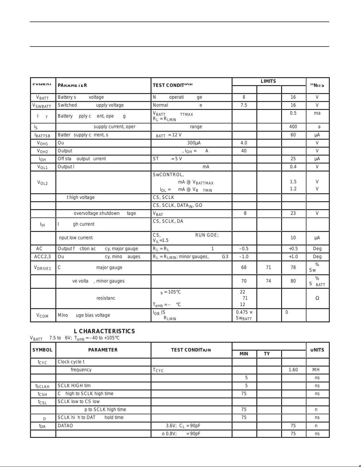
DC ELECTRICAL CHARACTERISTICS
V
= 8.0 to 16V; T
BATT
V
BATT
V
SWBATT
I
BATT
I
SWBATT
I
BATTSB
V
OH1
V
OH2
I
OH
V
OL1
V
OL2
V
IH
V
IL
V
OVSD
I
ÁÁ
IH
I
IL
ÁÁ
ACC1
ACC2,3
V
DRIVE1
ÁÁ
V
DRIVE2,3
R
LMIN
V
COM
Battery supply voltage
Switched battery supply voltage
Battery supply current, operating
Switched battery supply current, operating
Battery supply current, standby
Output high voltage
Output high voltage
Off state output current
Output low voltage
Output low voltage
Input high voltage
Input low voltage
Battery overvoltage shutdown voltage
Input high current
БББББББББ
Input low current
БББББББББ
Output function accuracy, major gauge
Output function accuracy, minor gauges
Coil drive voltage, major gauge
БББББББББ
Coil drive voltage, minor gauges
Minimum coil load resistance
Minor gauge bias voltage
= –40 to +105°C
amb
MIN
Normal operating range
Normal operating range
V
= V
BATT
RL = R
BATTMAX
LMIN
8
7.5
Normal operating range
V
= 12 V
BATT
DATA
SwCONTROL, IOH = 10µA
, IOH = 300µA
OUT
4.0
40
ST, VOH = 5 V
ST, DATA
, IOL = 1.5 mA
OUT
SwCONTROL,
IOL = 50 mA @ V
IOL = 20 mA @ V
CS, SCLK, DATAIN, GOE, RUN
BATTMAX
BATTMIN
3.5
CS, SCLK, DATAIN, GOE, RUN
V
BATT
CS, SCLK, DATAIN, RUN GOE;
ББББББББ
V
= 3.5
IH
18
ÁÁÁÁÁÁÁ
CS, SCLK, DATAIN, RUN GOE;
=1.5
V
IL
ББББББББ
RL = R
RL = R
ББББББББÁÁÁ
; major gauge, G1
LMIN
; minor gauges, G2 & G3
LMIN
ÁÁÁÁÁÁÁ
–0.5
–1.0
68
70
T
= 105°C
amb
T
= 25°C
amb
T
= –40°C
amb
IOB (Source or Sink)
R
= R
L
LMIN
226
171
127
0.475 ×
Sw
BATT
LIMITS
TYP
71
ÁÁ
74
MAX
16
16
0.5
400
60
25
0.4
1.5
1.2
1.5
23
10
10
+0.5
+1.0
78
Á
80
0.525 ×
Sw
BATT
V
V
ma
ma
µA
V
V
µA
V
V
V
V
V
V
µA
ÁÁ
µA
ÁÁ
Deg
Deg
%
ÁÁ
Sw
BATT
%
Sw
BATT
Ω
Ω
Ω
V
AC ELECTRICAL CHARACTERISTICS
V
BATT
F
t
SCLKL
t
SCLKH
1998 Apr 03
= 7.5 to 16V; T
t
CYC
SCLK
Clock cycle time
Clock frequency
SCLK LOW time
SCLK HIGH time
t
CSH
t
CSL
t
t
t
t
CS high to SCLK high time
SCLK low to CS low time
DATAIN setup to SCLK high time
SU
SCLK high to DATAIN hold time
HD
DATAOUT rise time
DR
DATAOUT fall time
DF
= –40 to +105°C
amb
T
CYC
0.8 to 3.6V; CL = 90pF
3.6 to 0.8V; CL = 90pF
4
MIN
625
175
175
75
75
75
75
LIMITS
TYP
MAX
1.60
75
75
ns
MHz
ns
ns
ns
ns
ns
ns
ns
ns

Philips Semiconductors Product specification
SA5778Serial triple gauge driver (STGD)
J1850
PROTOCOL
CONTROLLER
AU5780
J1850 VPW
TRANSCEIVER
J1850 BUS
80C51
MICRO–
CONTROLLER
ADDITIONAL GAUGE
DRIVERS; SA5775A
OR SA5777A
PROTECTED BY
SA5778
Figure 3. System Connections for the STGD
FUNCTIONAL DESCRIPTION
Figure 1 shows the pin-out of the STGD, which is packaged in an
SO-28 pin package, enhanced for improved thermal management.
Four pins on each side of the package serve as a heat spreader to
remove heat from the die, and also function as the ground
connection. The recommended mounting includes an area of copper
on the PC board to aid in thermal management.
Figure 2 is a block diagram of the STGD. A serial interface connects
the STGD to the microcontroller. A data output pin is provided to
permit the STGD to be wired in series with other Philips air core
gauge drivers such as the Serial Gauge Driver, SA5775, and the
Dual Gauge Driver, SA5777 or additional STGDs. Status information
may be passed back to the microcontroller via a status output, or via
the serial interface.
Figure 3 shows the connection of the STGD in a typical application.
GOE
SERIAL
SA5778
SERIAL
TRIPLE
GAUGE
DRIVER
MICROCONTROLLER
DATA
PORT N
DATA
5V
S
OUT
CLK
INT
4
2
2
V
IN
RUN
IGNITION
BATT
360° MAJOR
GAUGE
112° MINOR
GAUGE
SR01118
DATA
IN
S
CLK
CS
DATA
OUT
ST
DATA
IN
S
CLK
CS
DATA
OUT
ST
SA5778 SERIAL
TRIPLE
GAUGE DRIVER
ADDITIONAL
GAUGE DRIVER(S),
SA5775A,
SA5777A OR
SA5778
APPLICATION INFORMATION
Figure 4 demonstrates the connections between the STGD, the
microcontroller, and optionally additional gauge drivers such as the
SGD and DGD. With an active high on the chip select input (CS),
data is shifted into the STGD through DATA
. Several gauge drivers may be wired in series using a
S
CLK
common chip select and clock line, when more than three gauges
are needed. The DATA
pins are cascaded to the DATAIN pins of
OUT
the following gauge drivers. Status information can be returned to
the microcontroller via the ST pins of each gauge driver. These are
open-drain, active low outputs, which may be wire OR’ed together to
signal that a fault, such as a thermal shut down, has occurred within
one of the gauge drivers. This pin may be connected to a
microcontroller port pin for polling in software, or may be connected
to an external interrupt input to cause entry into an interrupt service
routine. The STGD, may also pass status information back to the
microcontroller serially. The rising edge of chip select loads status
information into the shift register for the first four bits that will be
shifted out of the STGD by the shift clock. Figure 11 shows the data
bits within the shift register. A low on the ST pin signals that one or
more status bits have been set in the status register. A high
indicates all status bits are reset. The status output bits include
minor gauge over current, major gauge over current, thermal
shutdown and RUN. Gauge data is captured in latches by the falling
edge of the chip select.
on the rising edge of
IN
SR01119
Figure 4. Serial Communications Between STGD,
Microcontroller and Other Gauge Drivers
Figure 5 shows the gauge connections to the STGD. The major
gauge, G1, supports full 360° operation with two coils driven. The
seven least significant bits of the gauge information are converted to
an analog level by digital-to-analog converter. The display range is
divided into eight sections, two sections per quadrant. The coils are
driven with a Sine/Cosine approximation. The three most significant
bits of gauge display information control the multiplexer to select
which coil is fed by the DAC and which coil receives a fixed bias.
The multiplexer also determines the polarity of the voltages supplied
to the coils.
The minor gauges, G2 and G3, each have one coil driven by a DAC.
The other coils of each gauge are wired in series with the switched
battery supply to supply the bias. The switched battery supply is
turned off during over voltage conditions. Only 9-bits of information
are required for the minor gauges, however, 10-bits are shifted
through the part to maintain compatibility with the SGD and DGD.
Hence, all gauges, both major and minor, are supplied with 10-bit
data for consistency.
1998 Apr 03
5
 Loading...