

Philips SA5777A Datasheet
INTEGRATED CIRCUITS
SA5777A
Dual air–core gauge driver
Product specification
Supersedes data of 1997 Feb 24
1999 Sep 20
Philips Semiconductors Product specification
SA5777ADual air-core gauge driver
DESCRIPTION
The SA5777A is a monolithic driver for controlling air-core (or
differential) meters typically used in automotive instrument cluster
applications. The circuit interfaces with a microprocessor through a
serial bus and directly drives the air-core meter. The SA5777A has
10-bit resolution (0.35 degree) and is guaranteed to be monotonic.
Data can be shifted through the part, allowing several SA5777As to
be cascaded with only one chip-select line. On-chip current shut
down logic protects the circuit from external faults.
FEATURES
•10-Bit resolution (0.35 degrees)
•Exceptional accuracy (0.5 degrees, typical)
•High-torque capability
•Active differential drivers eliminate back-EMF issues
•No RFI/EMI generation issues
•Simple serial interface
•Simple cascading capability for multiple meters
•Internal fault protection
•Only one external component required (bypass capacitor)
APPLICATION
•Instrumentation utilizing air-core meters
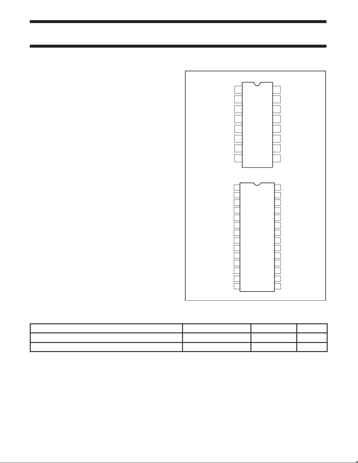
PIN CONFIGURATION
1
C1–
C1+
2
A
3
GND
4
V
BB
DATA
DATA
DATA
DATA
5
OUT
6
IN
V
7
CC
89
OE
1
C1–
C1+
2
3
NC
NC
4
5
NC
6
A
GND
7
V
BB
8
OUT
9
IN
10
NC
NC NC
11
12
NC NC
13
V
CC
OE
14
N Package
D Package
16
C2+
15
C2-
14
COM
13
A
GND
12
D
GND
11
ST
10
CS
S
CLK
28
C2+
C2-
27
NC
26
25
NC
24
COM
23
A
GND
NC
22
NC
21
20
D
GND
19
ST
18
17
16
CS
15
S
CLK
SL00460
Figure 1. Pin configuration
ORDERING INFORMATION
DESCRIPTION TEMPERATURE RANGE ORDER CODE DWG #
16-Pin Plastic Dual In-Line Package (DIP)
28-Pin Plastic Small Outline Package (SO)
1999 Sep 20 853-1930 022368
2
-40 to +85°C
-40 to +85°C
SA5777AN SOT38-4
SA5777AD SOT136-1
Philips Semiconductors Product specification
SA5777ADual air-core gauge driver
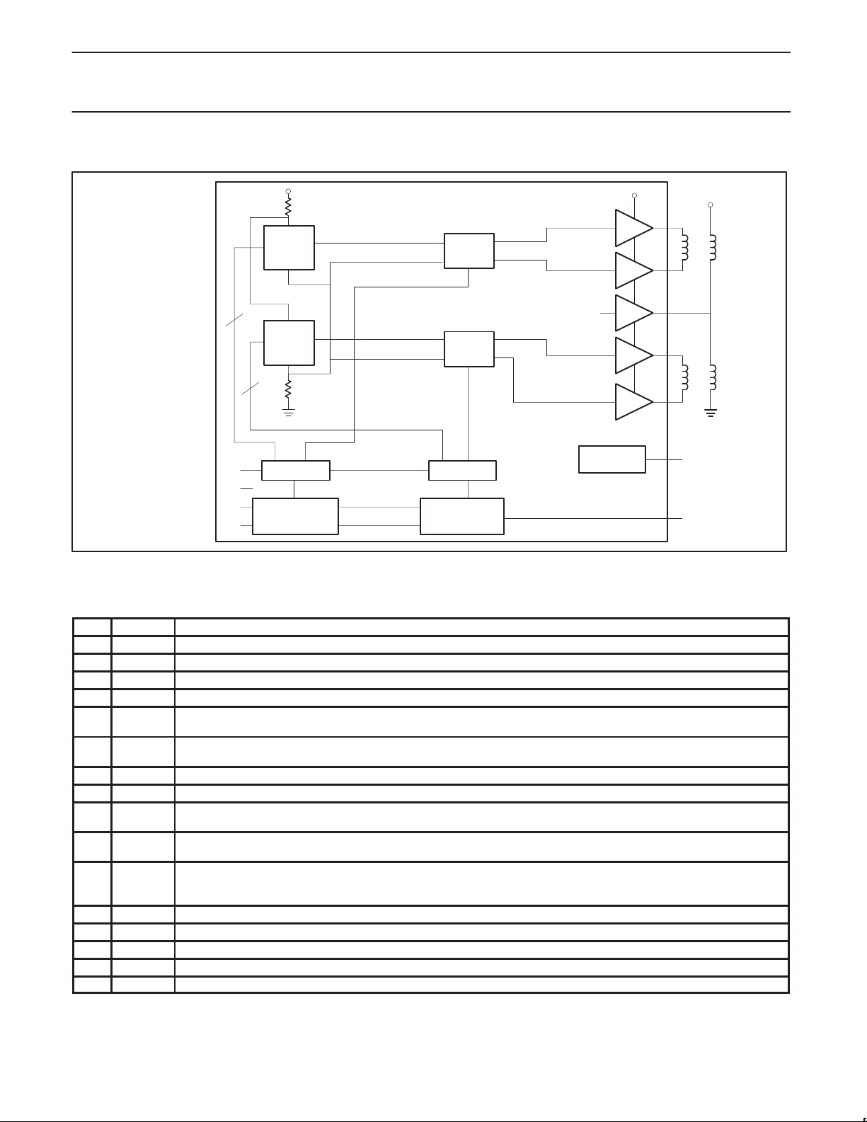
BLOCK DIAGRAM
V
7 + – BIT
DAC
BB
OE
MUX
C2+
C2–
V
BB
8
V
D
S
CS
CC
IN
CLK
7 + – BIT
DAC
8
9-BIT LATCH
10-BIT
SHIFT REGISTER
MUX
9-BIT LATCH
10-BIT
SHIFT REGISTER
Figure 2. Block diagram
Table 1. SA5777A Pin Descriptions for the N Package (Dual In-Line)
Pin # Name Function
1. C1– Negative output connection to the TAN coil of meter #1.
2. C1+ Positive output connection to the TAN coil of meter #1.
3. A
GND
4. V
DATA
5.
DATAINSerial data input. A new data word is serially shifted into the part on the rising edge of S
6.
7. V
8. OE Output drivers are turned off when this input is low.
S
9.
10.
CLK
CS Active high chip select input. When CS is high, the part is enabled to receive a new serial input word. The high-to-low
ST Status output. This is an open drain output and goes low when the coil output buffers (C1+, C1–, C2+, C2–, COM) have
11.
12. D
13. A
GND
GND
14. COM Output drive for biased coils. This output will be 1/2 of VBB.
15. C2– Negative output connection to the TAN coil of meter #2.
16. C2+ Positive output connection to the TAN coil of meter #2.
Ground for VBB supply. Pins 3, 12 and 13 should be connected on the circuit board.
Analog supply . Nominally 13.5 V.
BB
Serial data output. Output of the internal shift register. When a new data word is shifted in, the old word is shifted out the
OUT
DATA
pin. DATA
OUT
output is always active.
OUT
first, gauge 1 first.
5 V logic supply. The internal latches and registers are set to zero on the rising edge of this signal.
CC
Serial clock input. Data is loaded into the part on the rising edge of S
edge of S
CLK
.
transition of CS loads the new 20-bit word into the DAC registers and updates the output.
been disabled. The coil outputs may be disabled due to shorted outputs, over-temperature conditions, power-on reset,
or by the output enable (OE) pin. Multiple status outputs , ST, may be wire OR’ed together.
Ground for VCC supply. Connect to Pins 3 and 13.
Ground for VBB supply. Connect to Pins 3 and 12.
VBB/2
FAULT
DETECTION
. The data is shifted in MSB
CLK
. Data is shifted out of DATA
CLK
COM
C1+
C1–
ST
D
SL00461
OUT
OUT
on the falling
1999 Sep 20
3

Philips Semiconductors Product specification
SA5777ADual air-core gauge driver
Table 2. SA5777A Pin Descriptions for the D Package (Small Outline)
Pin # Name Function
1. C1– Negative output connection to the TAN coil of meter #1.
2. C1+ Positive output connection to the TAN coil of meter #1.
3. NC No connect
4. NC No connect
5. NC No connect
6. A
GND
7. V
DATA
8.
DATAINSerial data input. A new data word is serially shifted into the part on the rising edge of S
9.
10. NC No connect
11. NC No connect
12. NC No connect
13. V
14. OE Output drivers are turned off when this input is low.
S
15.
16.
CLK
CS Active high chip select input. When CS is high, the part is enabled to receive a new serial input word. The high-to-low
17. NC No connect
18. NC No connect
ST Status output. This is an open drain output and goes low when the coil output buffers (C1+, C1–, C2+, C2–, COM) have
19.
20. D
GND
21. NC No connect
22. NC No connect
23. A
GND
24. COM Output drive for biased coils. This output will be 1/2 of VBB.
25. NC No connect
26. NC No connect
27. C2– Negative output connection to the TAN coil of meter #2.
28. C2+ Positive output connection to the TAN coil of meter #2.
Ground for VBB supply. Pins 6, 20 and 23 should be connected on the circuit board.
Analog supply . Nominally 13.5 V.
BB
Serial data output. Output of the internal shift register. When a new data word is shifted in, the old word is shifted out
OUT
the DATA
first, gauge 1 first.
5 V logic supply. The internal latches and registers are set to zero on the rising edge of this signal.
CC
Serial clock input. Data is loaded into the part on the rising edge of S
edge of S
pin. DATA
OUT
.
CLK
output is always active.
OUT
. The data is shifted in MSB
CLK
. Data is shifted out of DATA
CLK
transition of CS loads the new 20-bit word into the DAC registers and updates the output.
been disabled. The coil outputs may be disabled due to shorted outputs, over-temperature conditions, power-on reset,
or by the output enable (OE) pin. Multiple status outputs , ST, may be wire OR’ed together.
Ground for VCC supply. Connect to Pins 6 and 23.
Ground for VBB supply. Connect to Pins 6 and 20.
on the falling
OUT
ABSOLUTE MAXIMUM RATINGS
SYMBOL PARAMETER RATING UNIT
V
BB
V
CC
V
IN
D
to A
T
T
T
P
θ
GND
A
J
STG
D
JA
GND
NOTE:
1. For power dissipation ratings in still air, derate above 25°C at the following rates:
N and D packages at 12mW/°C
1999 Sep 20
Analog supply -1 to +23 V
Digital supply -1 to +6 V
Digital input voltage, Data In, OE, CS, S
CLK
-1 to +6 V
Ground difference ±0.5 V
Ambient operating temperature –40 to +85
Junction temperature 150
Storage temperature –65 to +150
1
Power dissipation (TA = 25°C)
N, D packages 1500 mW
DIP and SO packages 90
4
°C
°C
°C
°C/W
 Loading...