

Page 1
查询SA57031-18UK供应商
INTEGRATED CIRCUITS
SA57031-XX
Micropower 150 mA, low-noise, low dropout
linear regulator with on/off
Product data
Supersedes data of 2003 Feb 24
2003 Jun 23
Page 2
Philips Semiconductors Product data
Micropower 150 mA, low-noise, low dropout linear
regulator with on/off
GENERAL DESCRIPTION
The SA57031 is a 150 mA, fixed output voltage regulator designed
to provide very low dropout voltage and low noise in battery
powered and portable applications. The output voltage is preset to
voltages between 1.8 to 5.0 Volts, in 100 mV increments.
The SA57031 achieves excellent performance in all specifications
such as excellent power supply ripple rejection at low frequency, low
supply-current, low dropout voltage, low power consumption,
extremely small size with chip scaled package (CSP), extremely low
output noise voltage, very fast start-up response time, precision
output, fast dynamic response to line and load regulation, etc. This
regulator consists of an internal voltage reference, and current limit.
The SA57031 is housed in a WL-CSP4 package (see dimensional
drawing for layout).
FEATURES
•Many Preset Output Voltages: 1.8 to 5.0 V in 0.1 V increments
•Wafer-level chip scale package (WL-CSP4)
•Extremely low PSRR: 80 dB typical at 1 kHz
•Low Dropout Voltage: 100 mV (typ) @ 50 mA output current
•Very Low Consumption Current: 100 mA typ. (when not loaded),
0.1 mA max. (when off)
•High precision Output Voltage: ±2%
•Output Current Capacity: 150 mA (typ)
•Low Noise: 30mVrms @ 10 Hz to 100 kHz
•Good Line Regulation: 0.01%/V typ.
•Good Load Regulation: 0.003%/mA typ.
•Low T emperature Drift Co-ef ficient to V
•Built-in Current Limiter
•Wide Operating Temperature Range: –40 to +85 °C
APPLICATIONS
•Cellular Phones, Cordless Phones and 2-way Radios
•Electronic Notebooks, PDAs and Palmtop Computers
•Cameras, VCRs and Camcorders
•PCMCIA Cards
•Modems
•Battery-powered or Hand-held Instruments
Bottom View
SA57031-XX
: ±100 ppm/°C
O
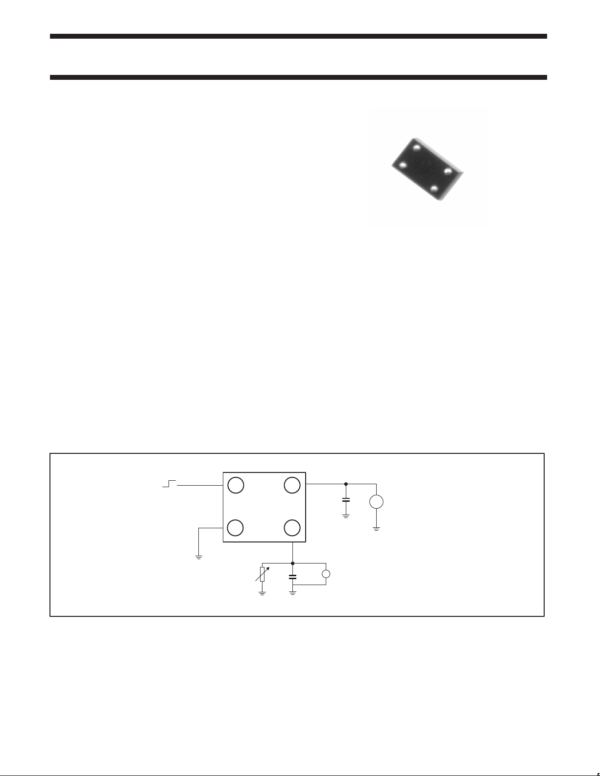
SIMPLIFIED SYSTEM DIAGRAM (BOTTOM VIEW)
ON
OFF
A2
SA57031-XX
GND
A1 B1
R
LOAD
Figure 1. Simplified system diagram.
V
I
B2
V
O
C
I
2.2 µF
Preset output voltages:
V
C
O
1.8 V to 5.0 V
(in 100 mV increments)
+
DC
2.0 V TO 6.0 V
–
SL02001
2003 Jun 23 853-2361 28634
2
Page 3
Philips Semiconductors Product data
TYPE NUMBER
Micropower 150 mA, low-noise, low dropout linear
SA57031-XX
regulator with on/off
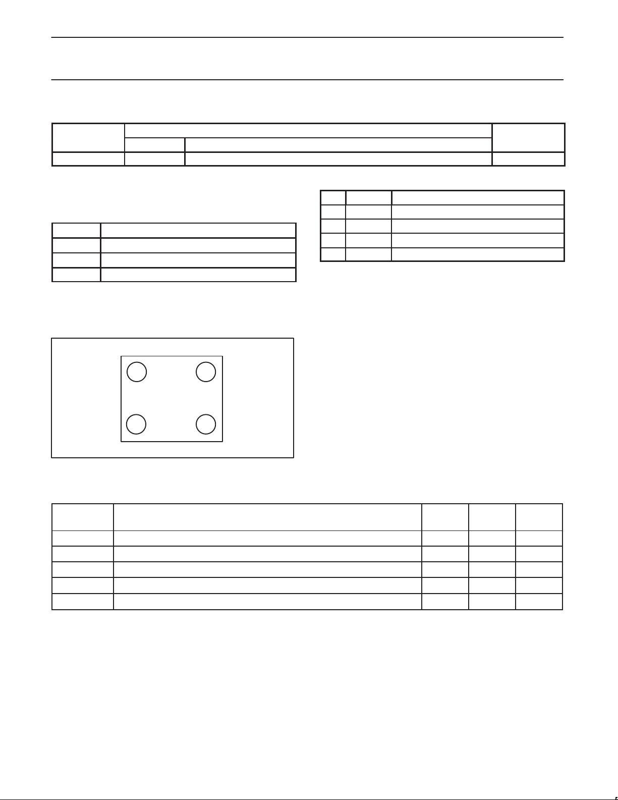
ORDERING INFORMATION
PACKAGE
NAME DESCRIPTION
SA57031-XXUK WL–CSP4 wafer level, chip-scale package; 4 bumps –40 to +85 °C
NOTE:
The device has five voltage output options, indicated by the XX on
the Type Number. Other voltages, between 2.5 to 5.0 V in 100 mV
increments, are available on request.
XX
18 1.8 V
24 2.4 V
28 2.8 V
VOLTAGE (Typical)
PIN DESCRIPTION
PIN SYMBOL DESCRIPTION
A1 GND Device ground
B1 VO V oltage output
B2 VI Voltage input
A2 ON/OFF Control pin. Connect to VI if not used.
PIN CONFIGURATION (TOP VIEW)
TEMPERATURE
RANGE
ON/OFF
A2
SA57031-XX
A1 B1
GND
Figure 2. Pin configuration.
V
B2
V
I
O
SA00633
MAXIMUM RATINGS
Symbol
Tstg Storage temperature range –40 +150 °C
Toper Operating Temperature Range –40 +85 °C
VI Supply voltage –0.3 +7 V
IO Output Current
P Power dissipation
Parameter
Min Max Unit
–
–
200 mA
190 mW
2003 Jun 23
3
Page 4
Philips Semiconductors Product data
PSRR
Power supply ripple rejection
dB
Micropower 150 mA, low-noise, low dropout linear
regulator with on/off
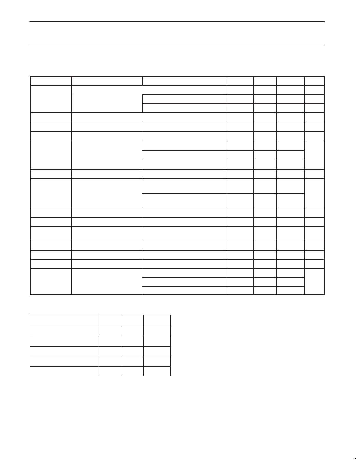
CHARACTERISTICS
Tamb = 25 °C; VI = V
SYMBOL
I
CC
I
(OFF) Input current (off) VON/OFF = 0.25 V
CC
Iq Quiescent Current IO = 0 to 150 mA
∆V
LNR
∆V
LDR
∆VO/∆T VO Temperature coefficient Tj = –30 to +85 °C
Vn Output noise voltage fBW = 20 to 80 kHz; CO = 2.2 µF
I
ON/OFF
V
ON/OFF(H)
V
ON/OFF(L)
R
ON/OFF
V
O
V
dropout
(nom) +1 V; VON/OFF = 2 V; IO = 1 mA unless otherwise specified.
O
PARAMETER CONDITIONS MIN. TYP. MAX. UNIT
No-load input current
Line regulation VI = VO +0.5 V to 6 V
Load regulation
pp
pp
Output short-circuit current VI = VO +1 V ; VO = 0 V
ON/OFF HIGH threshold
voltage
ON/OFF LOW threshold voltage 0
ON/OFF Pull-down resistance 2.5 5 15 MΩ
Output voltage (nominal) x0.98 nom x1.02 V
Dropout voltage
IO = 0 mA
IO = 50 mA – 55 –
IO = 150 mA – 60 –
IO = 1 to 50 mA
IO = 1 to 100 mA
IO = 1 to 150 mA
f = 1 kHz; IO = 1 mA; Vripple = 0.5 V ;
= 1.8 to 4.0 V
V
O
f = 1 kHz; IO = 1 mA; Vripple = 0.5 V ;
= 4.1 to 5.0 V
V
O
VO = 2.0 to 2.3 – 0.25 0.35
VO = 2.4 to 2.7 – 0.24 0.29
VO = 2.8 to 5.0 – 0.23 0.26
SA57031-XX
–
–
–
–
–
–
–
– –
–
–
–
–
1.5
45 100 µA
0.1 1 µA
100 190 µA
5 10 mV
10 25
20 50
30 70
80
70
30
30
–
–
mV
ppm/°C
–
–
–
–
VI V
0.25 V
µVrms
mA
V
PRESET OUTPUT VOLTAGES
Part Number Min Typ Max
SA57031-25UK 2.450 2.500 2.550
SA57031-28UK 2.744 2.800 2.856
SA57031-30UK 2.940 3.000 3.060
SA57031-33UK 3.234 3.300 3.366
SA57031-36UK 3.528 3.600 3.672
2003 Jun 23
4
Page 5
Philips Semiconductors Product data
Micropower 150 mA, low-noise, low dropout linear
regulator with on/off
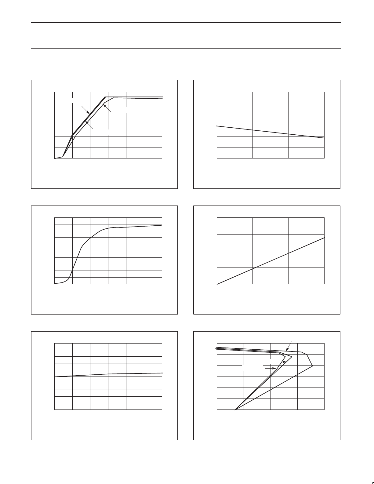
TYPICAL PERFORMANCE CURVES
Shown for the SA57031-28UK only; T
3.0
IO = 1mA
2.5
2.0
1.5
1.0
OUTPUT VOLTAGE (V)
0.5
0
0123456
IO = 30 mA
INPUT VOLTAGE VI(V)
Figure 3. Output voltage versus input voltage.
= 25 °C; VI = VO + 1 V; V
amb
IO = 100 mA
SL01970
= VI; Cin = 2.2 µF, C
On/Off
LOAD REGULATION Vload(mV)
150
100
–50
–100
–150
SA57031-XX
= 2.2 µF unless otherwise specified
O
50
0
0 50 100 150
OUTPUT CURRENT IO(mA)
Figure 6. Load regulation versus load current.
SL01973
50
µ
45
( A)
40
DD
35
30
25
20
15
10
5
NO-LOAD INPUT CURRENT I
0
0123456
INPUT VOLTAGE VI(V)
Figure 4. No-load input current versus input voltage.
1.0
0.8
0.6
0.4
0.2
–0.0
–0.2
–0.4
–0.6
LINE REGULATION Vline (mV)
–0.8
–1
3 3.5 4.0 4.5 5.0 5.5 6.0
IO = 30 mA
SL01971
0.4
0.3
0.2
0.1
DROPOUT VOLTAGE Vio(V)
0
0 50 100 150
VI = 2.6 V, IO = 10 mA
OUTPUT CURRENT IO(mA)
Figure 7. Dropout voltage versus output current.
3.0
2.5
2.0
1.5
1.0
OUTPUT VOLTAGE Vo(V)
0.5
0
0 100 200 300 400
VI = 5.0 V
VI = 6.0 V
VI = 3.8 V
SL01974
Figure 5. Line regulation versus input voltage.
2003 Jun 23
INPUT VOLTAGE VI(V)
SL01972
OUTPUT CURRENT IO(mA)
SL01975
Figure 8. Current limit versus output current.
5
Page 6
Philips Semiconductors Product data
Micropower 150 mA, low-noise, low dropout linear
regulator with on/off
100
µ
90
( A)
80
70
60
50
40
GND PIN CURRENT
30
20
10
0
0 25 50 75 100 125 150
OUTPUT CURRENT (mA)
SL01976
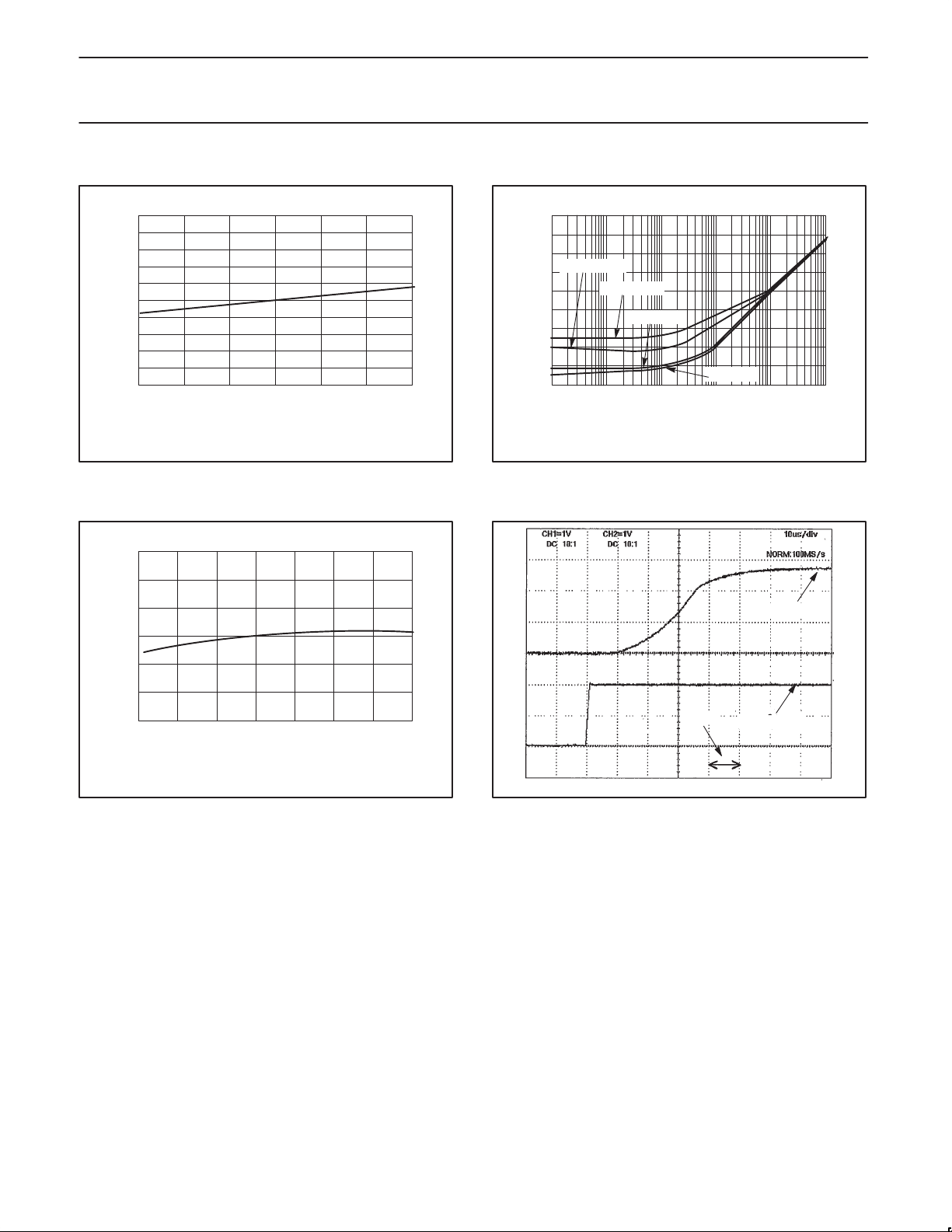
Figure 9. Ground pin current.
–10
–20
–30
–40
–50
–60
–70
RIPPLE REJECTION (dB)
–80
–90
SA57031-XX
0
IO = 100 mA
IO = 150 mA
IO = 30 mA
IO = 1 mA
0.01 0.10 1.00 10.00 100.00 1000.00
FREQUENCY (kHz)
SL01978
Figure 11. Ripple rejection.
2.84
2.82
2.80
2.78
2.76
OUTPUT VOLTAGE Vo(V)
2.74
2.72
–50 –25 0 25 50 75 100 125
TEMPERATURE T(°C)
SL01977
Figure 10. Output voltage versus ambient temperatures.
10 µS
V
on/off
Figure 12. On/off control pin.
VO = 2.8 V
= 2 V
SL01991
2003 Jun 23
6
Page 7
Philips Semiconductors Product data
Micropower 150 mA, low-noise, low dropout linear
regulator with on/off
VI = 4.8 V
VI = 3.8 V
200 µS
VI = 2 V/div
VO = 10 mV/div
SL01992
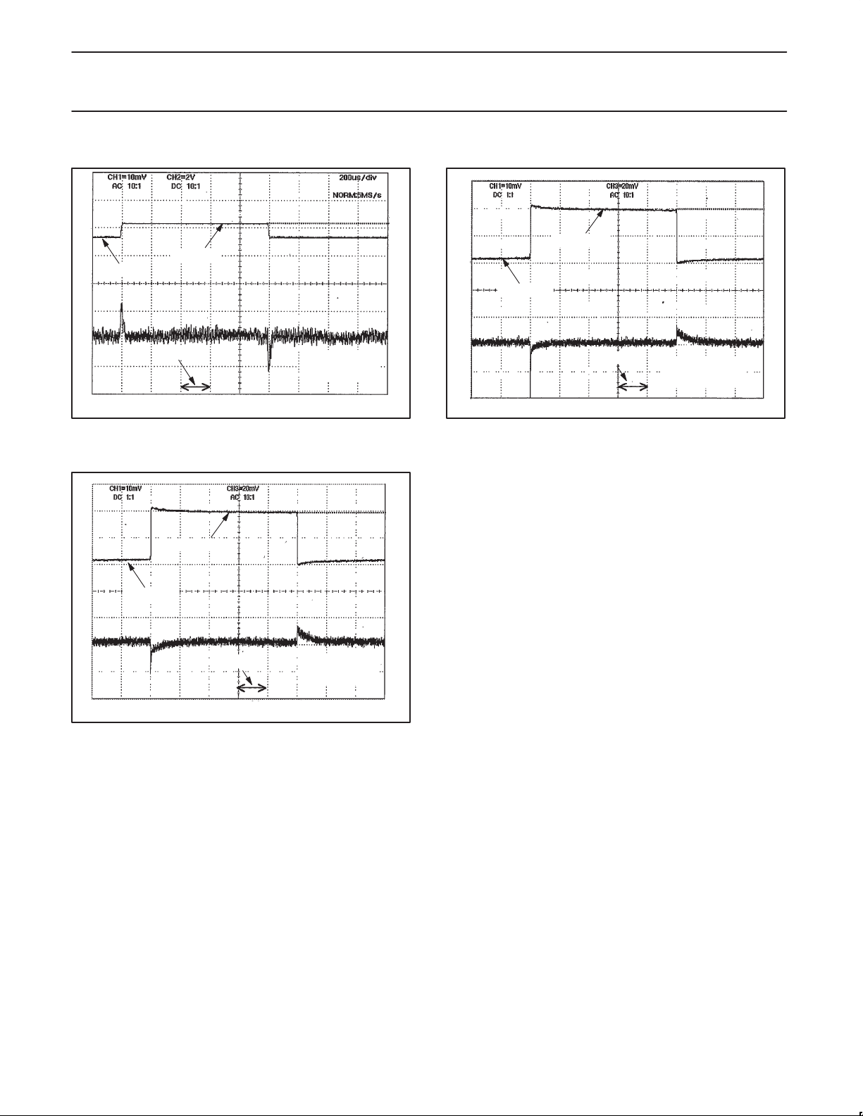
Figure 13. Line transient response.
SA57031-XX
IO = 100 mA
IO = 0.1 mA
500 µS
Figure 15. Load transient response.
C
= 1.0 µF
O
IO = 50 mA/div
VO = 10 mV/div
SL01994
IO = 100 mA
IO = 0.1 mA
500 µS
Figure 14. Load transient response.
C
= 2.2 µF
O
IO = 50 mA/div
VO = 10 mV/div
SL01993
2003 Jun 23
7
Page 8
Philips Semiconductors Product data
Micropower 150 mA, low-noise, low dropout linear
regulator with on/off
TECHNICAL DISCUSSION
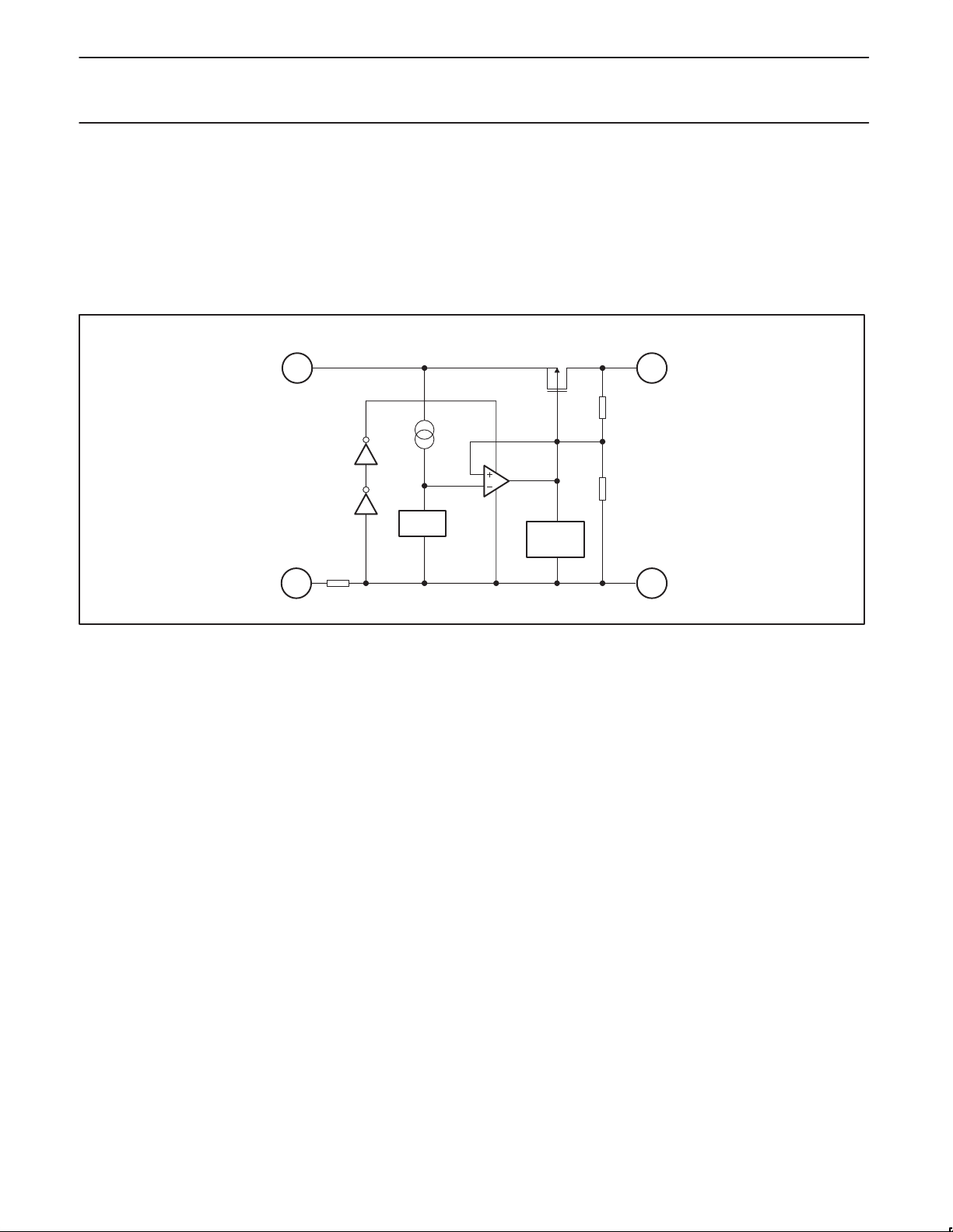
As illustrated in Figure 16, the SA57031 consists of a band-gap
voltage reference, an error amplifier, P-channel pass transistor ,
current limit circuit and an internal feedback voltage divider. The
output voltage is fed back through an internal resistor voltage divider
connected to the V
O pin.
The reference is connected to the error amplifier’s inverting input.
The error amplifier compares the reference with the feedback
SA57031-XX
V
3
I
V
REF
voltage and amplifies the difference. If the feedback voltage is lower
than the reference voltage, the pass transistor’s gate is pulled lower,
which allows more current to pass to the output and increase the
output voltage. If the feedback voltage is too high, the pass
transistor gate is pulled up, allowing less current to pass to the
output, resulting in a decrease in output voltage.
CURRENT
LIMITER
SA57031-XX
2
V
O
ON/OFF
4 1
Figure 16. Block diagram (bottom view).
GND
SA00634
2003 Jun 23
8
Page 9
Philips Semiconductors Product data
Micropower 150 mA, low-noise, low dropout linear
regulator with on/off
APPLICATION INFORMATION
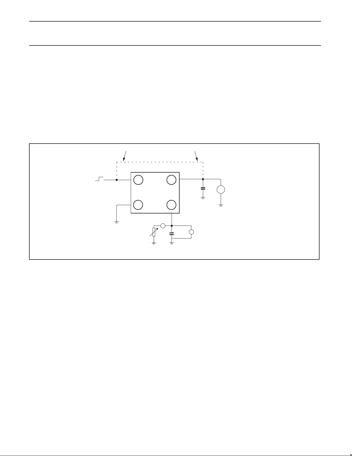
The following points have to be kept in mind for good performance
while using these devices.
Input Capacitor
An input capacitor of 2.2 µF is required between the SA57031 input
pin and the circuit ground. This capacitor must be located as close
as possible to the V
I or GND pin (not more than 1 cm away from the
pin) and returned to a clean analog ground. Any good quality
ceramic, tantalum, or film capacitor will work.
Output Capacitor
Phase compensation is used for securing stable operation even if
the load current varies. For this reason, an output capacitor with
ON/OFF PIN MUST BE ACTIVELY TERMINATED
ON
OFF
A2
SA57031-XX
GND
A1 B1
good frequency characteristics is needed. Set it as close to the
circuit as possible and make the wiring as short as possible. The
value of the output capacitance has to be at least 2.2µF and has to
have B-type temperature characteristics.
ON/OFF (Chip Enable) Pin
The ON/OFF pin must be actively terminated, not floating. If the
function is not needed, the pin should be tied to V
enable the device.
Line Impedance of VI and GND
The VI and GND lines should be sufficiently wide to minimize
impedance. If the impedance of these lines is high, there is a chance
to pick up noise or malfunction.
V
I
B2
2.2 µF
C
I
+
DC
2.0 V TO 6.0 V
–
SA57031-XX
I to permanently
V
O
R
LOAD
A
V
C
O
C
= 2.2 mF for VO = 2.5 to 5.0 V
O
CO = 4.7 mF for VO = 1.8 to 2.5 V
Figure 17. Typical application circuit.
SA00632
2003 Jun 23
9
Page 10
Philips Semiconductors Product data
Micropower 150 mA, low-noise, low dropout linear
regulator with on/off
PACKING METHOD
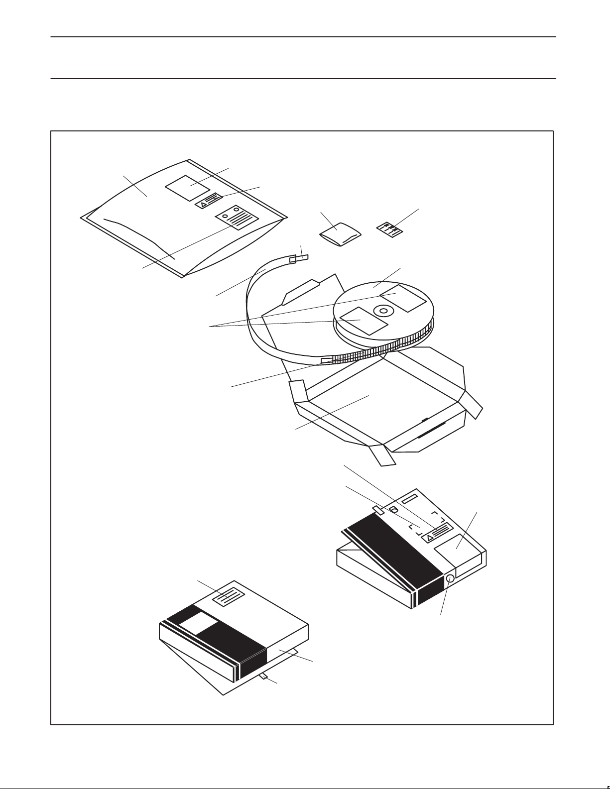
The SA57031-XX is packed in reels, as shown in Figure 18.
BAG
MOISTURE CAUTION
PRINT
GUARD BAND
BARCODE LABEL
BARCODE LABEL
ESD PRINT
DRY-AGENT
TAPE
RELATIVE HUMIDITY
INDICATOR
REEL ASSEMBLY
SA57031-XX
ESD EMBOSSED
PRE-PRINTED HYATT PATENT
PRINTED PLANO BOX
PRINTED ESD WARNING
SPACE FOR ADDITIONAL LABEL
BARCODE LABEL
DRYPACK ID STICKER
PRINTED PLANO BOX
2003 Jun 23
QA SEAL
SL01962
Figure 18. Tape and reel packing method
10
Page 11
Philips Semiconductors Product data
Micropower 150 mA, low-noise, low dropout linear
regulator with on/off
TAPE PULL OUT DIRECTION
T
B0
K
A0
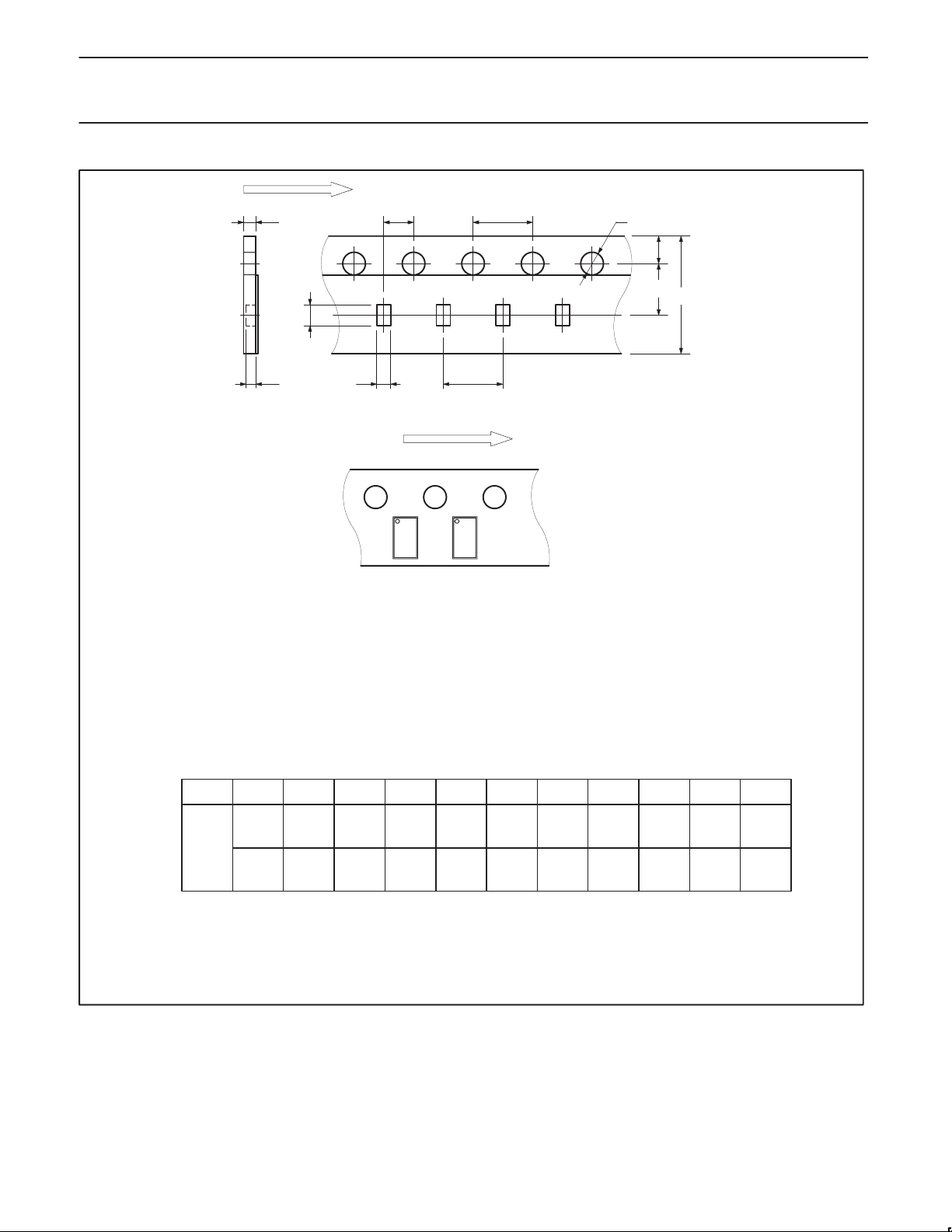
NOTES:
1. IC pull out direction
B HOUSING
P2 P0
P1
TAPE PULL OUT DIRECTION
TOP VIEW
SA57031-XX
D0
E
F
W
2. Carrier tape material:
paper type, with ESD protection.
3. The length of the leader:
More than 400 mm which include 40 holes or more without any products.
IT’s must have the top cover tape.
4. The length of trailer:
More than 40 mm which include without any products.
IT’s must have the top copy tape.
The end of trailer must be detached from reel.
UNIT A0 B0 W F E P1 P2
0.90 1.40 8.0 3.5 1.75 4.0 2.0
mm
"0.03 "0.03 "0.1 "0.05 "0.05 "0.05 "0.05 "0.1 "0.03 "0.03 "0.03
P0
ΘD0
4.0
1.55T0.60K0.58
SL02002
2003 Jun 23
11
Page 12
Philips Semiconductors Product data
Micropower 150 mA, low-noise, low dropout linear
regulator with on/off
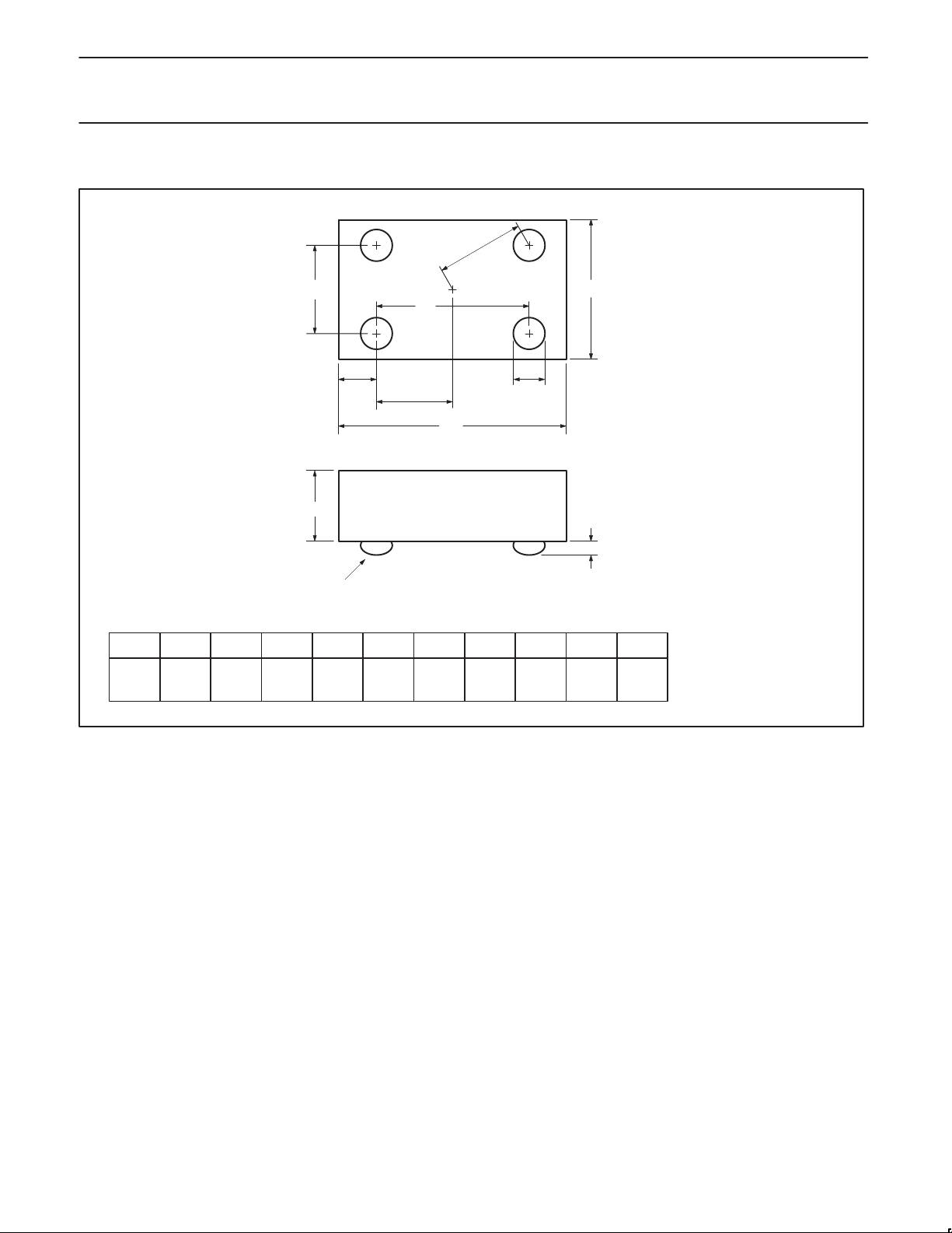
WL-CSP4: wafer level, chip-scale package; 4 bumps
X3
X4
X5
X6
X7
X1
X9
X8
SA57031-XX
X2
BUMP
DIMENSIONS (mm are the original dimensions)
UNIT X1 X2 X3 X4 X5 X6 X7
mm
1.32
1.26
0.82
0.76
0.5 0.5 0.866 0.212 0.433
X8
0.23
0.13
X9
0.42
0.38
X10
X10
0.10
0.06
SL02098
2003 Jun 23
12
Page 13
Philips Semiconductors Product data
Micropower 150 mA, low-noise, low dropout linear
SA57031-XX
regulator with on/off
REVISION HISTORY
Rev Date Description
_2 20030623 Product data (9397 750 11664); ECN 853-2361 30063 dated 23 June 2003.
_1 20030224 Product data (9397 750 11001); ECN 853-2361 28634 dated 2002 Jul 18
Data sheet status
Level
I
II
III
[1] Please consult the most recently issued data sheet before initiating or completing a design.
[2] The product status of the device(s) described in this data sheet may have changed since this data sheet was published. The latest information is available on the Internet at URL
[3] For data sheets describing multiple type numbers, the highest-level product status determines the data sheet status.
Data sheet status
Objective data
Preliminary data
Product data
http://www.semiconductors.philips.com.
Supersedes SA57031-XX_1 (9397 750 11001) of 2003 Feb 24.
Modifications:
•WL-CSP4 package outline dimensional drawing modified.
[1]
Product
[2] [3]
status
Development
Qualification
Production
Definitions
This data sheet contains data from the objective specification for product development.
Philips Semiconductors reserves the right to change the specification in any manner without notice.
This data sheet contains data from the preliminary specification. Supplementary data will be published
at a later date. Philips Semiconductors reserves the right to change the specification without notice, in
order to improve the design and supply the best possible product.
This data sheet contains data from the product specification. Philips Semiconductors reserves the
right to make changes at any time in order to improve the design, manufacturing and supply. Relevant
changes will be communicated via a Customer Product/Process Change Notification (CPCN).
Definitions
Short-form specification — The data in a short-form specification is extracted from a full data sheet with the same type number and title. For detailed information see
the relevant data sheet or data handbook.
Limiting values definition — Limiting values given are in accordance with the Absolute Maximum Rating System (IEC 60134). Stress above one or more of the limiting
values may cause permanent damage to the device. These are stress ratings only and operation of the device at these or at any other conditions above those given
in the Characteristics sections of the specification is not implied. Exposure to limiting values for extended periods may affect device reliability.
Application information — Applications that are described herein for any of these products are for illustrative purposes only. Philips Semiconductors make no
representation or warranty that such applications will be suitable for the specified use without further testing or modification.
Disclaimers
Life support — These products are not designed for use in life support appliances, devices, or systems where malfunction of these products can reasonably be
expected to result in personal injury . Philips Semiconductors customers using or selling these products for use in such applications do so at their own risk and agree
to fully indemnify Philips Semiconductors for any damages resulting from such application.
Right to make changes — Philips Semiconductors reserves the right to make changes in the products—including circuits, standard cells, and/or software—described
or contained herein in order to improve design and/or performance. When the product is in full production (status ‘Production’), relevant changes will be communicated
via a Customer Product/Process Change Notification (CPCN). Philips Semiconductors assumes no responsibility or liability for the use of any of these products, conveys
no license or title under any patent, copyright, or mask work right to these products, and makes no representations or warranties that these products are free from patent,
copyright, or mask work right infringement, unless otherwise specified.
Contact information
For additional information please visit
http://www.semiconductors.philips.com . Fax: +31 40 27 24825
For sales offices addresses send e-mail to:
[email protected].
Document order number: 9397 750 11664
Koninklijke Philips Electronics N.V. 2003
All rights reserved. Printed in U.S.A.
Date of release: 06-03
2003 Jun 23
13
 Loading...