

Page 1

查询SA56614-20供应商查询SA56614-20供应商
INTEGRATED CIRCUITS
SA56614-XX
CMOS system reset
Product data
Supersedes data of 2001 Apr 24
File under Integrated Circuits, Standard Analog
2001 Jun 19
Page 2

Philips Semiconductors Product data
SA56614-XXCMOS system reset
GENERAL DESCRIPTION
The SA56614-XX is a CMOS device designed to generate a reset
signal for a variety of microprocessor and logic systems. Accurate
reset signals are generated during momentary power interruptions,
or whenever power supply voltages sag to intolerable levels.
Several reset threshold versions of the device are available. A
totem-pole output topology is incorporated to provide both current
source and sink capability to the user.
SA56614-XX is available in the SOT23-5 surface mount package.
FEA TURES
•12 V
maximum operating voltage
DC
•Low operating voltage (0.65 V)
•Totem pole CMOS output
•Offered in reset thresholds of
2.0, 2.7, 2.8, 2.9, 3.0, 3.1, 4.2, 4.3, 4.4, 4.5, 4.6, 4.7 V
•Available in SOT23-5 surface mount package
SIMPLIFIED SYSTEM DIAGRAM
V
DD
V
REF
R
V
SS
V
2
R
R
3
V
DC
DD
NE56614-XX
SS
APPLICATIONS
•Microcomputer systems
•Logic systems
•Battery monitoring systems
•Back-up power supply circuits
•Voltage detection circuits
V
OUT
1
RESET
V
CPU
V
SS
SL01343
DD
Figure 1. Simplified system diagram.
2001 Jun 19 853–2248 26559
2
Page 3

Philips Semiconductors Product data
TYPE NUMBER
SA56614-XXCMOS system reset
ORDERING INFORMATION
PACKAGE
NAME DESCRIPTION
SA56614-XXGW SOT23-5, SOT25, SO5 plastic small outline package; 5 leads (see dimensional drawing) –40 to +85 °C
TEMPERATURE
RANGE
NOTE:
The device has twelve detection voltage options, indicated by the
XX on the ‘Type number’.
XX
DETECT VOLTAGE (Typical)
20 2.0 V
27 2.7 V
28 2.8 V
29 2.9 V
30 3.0 V
31 3.1 V
42 4.2 V
43 4.3 V
44 4.4 V
45 4.5 V
46 4.6 V
47 4.7 V
PIN CONFIGURATION
1
V
OUT
2
V
DD
SS
SA56614-XX
34
5 N/C
N/CV
Part number marking
Each package is marked with a four letter code. The first three
letters designate the product. The fourth letter, represented by ‘x’, is
a date tracking code. For example, AALB is device AAW (the
SA56614-28 reset) produced in time period ‘B’.
Part number
Marking
SA56614-20 A A U x
SA56614-27 A A V x
SA56614-28 A A W x
SA56614-29 A A X x
SA56614-30 A A Y x
SA56614-31 A A Z x
SA56614-42 A B A x
SA56614-43 A B B x
SA56614-44 A B C x
SA56614-45 A B D x
SA56614-46 A B E x
SA56614-47 A B F x
PIN DESCRIPTION
PIN SYMBOL DESCRIPTION
1 V
2 V
3 V
OUT
DD
SS
4 N/C No connection.
5 N/C No connection.
Reset HIGH output.
Positive supply.
Ground. Negative supply.
MAXIMUM RATINGS
2001 Jun 19
SL01360
Figure 2. Pin configuration.
SYMBOL PARAMETER MIN. MAX. UNIT
V
V
I
OUT
T
T
DD
OUT
oper
stg
Power supply voltage –0.3 12 V
Output voltage – VSS – 0.3 V
Output current – 50 mA
Operating temperature –40 85 °C
Storage temperature –40 125 °C
P Power dissipation – 150 mW
3
Page 4

Philips Semiconductors Product data
1
Fig. 17
SA56614-XXCMOS system reset
DC ELECTRICAL CHARACTERISTICS
Characteristics measured with T
SYMBOL
V
S
∆V
S
Reset detection threshold VS – 2% V
Hysteresis VDD = 0 V → VS + 1.0 V → 0 V
PARAMETER CONDITIONS TEST
VS/∆T Threshold voltage temperature
coefficient
I
CC
I
OH
I
NDS1
I
NDS2
I
NDS3
I
PDS1
I
PDS2
I
PDS3
Supply current VDD = VS + 1.0 V – 0.25 1.0 µA
IDS leakage current when OFF VDD = VDS = 10 V 3
N-channel IDS output sink current 1 VDD = 1.2 V; VDS = 0.5 V –0.23 –1.4 – mA
N-channel IDS output sink current 2
(for VS > 2.6 V)
N-channel IDS output sink current 3
(for VS > 3.9 V)
P-channel IDS output source current 1
(for VS < 4.0 V)
P-channel IDS output source current 2
(for VS < 5.7 V)
P-channel IDS output source current 3
(for V
< 5.7 V)
S
= 25 °C, unless otherwise specified.
amb
–40 °C ≤ T
VDS = 0.5 V; VDD = 2.4 V
VDS = 0.5 V; VDD = 3.6 V
VDS = 0.5 V; VDD = 4.8 V 0.36 2.1 – mA
VDS = 0.5 V; VDD = 6.0 V;
4.0 V < VS < 5.7 V
VDS = 0.5 V; VDD = 8.4 V 0.59 3.3 – mA
≤ +85 °C
amb
CIRCUIT
Fig. 16
Fig. 18
2
Fig. 17
3
Fig. 18
MIN. TYP. MAX. UNIT
VS + 2% V
S
VS × 0.03 VS × 0.05 VS × 0.08 V
– ±0.01 – %/°C
– – 0.1 µA
–1.6 –8.3 – mA
–3.2 –14.7 – mA
0.46 2.5 – mA
2001 Jun 19
4
Page 5

Philips Semiconductors Product data
SA56614-XXCMOS system reset
TYPICAL PERFORMANCE CURVES
0.50
VDD = VS + 1.0 V
0.45
NORMALIZED TO 25 °C
0.40
0.35
0.30
0.25
, SUPPLY CURRENT (mA)I
0.20
DD
0.15
0.10
–50 –25 0 25 50 75 100 125
T
, TEMPERATURE (°C)
amb
Figure 3. Supply current versus temperature.
SL01344
+0.20
VCC FALLING
+0.15
VS NORMALIZED TO 25 °C
+0.10
+0.05
V
S
–0.05
–0.10
, NORMALIZED THRESHOLD (V)V
S
–0.15
–0.20
–50 –25 0 25 50 75 100 125
T
, TEMPERATURE (°C)
amb
Figure 4. Detection threshold versus temperature.
SL01345
200
V
= VSH – V
S(HYS)
(VCC RISING – VCC FALLING)
150
100
, DETECTION HYSTERESIS (mV)V
50
S(HYS)
0
–50 –25 0 25 50 75 100 125
SL
T
, TEMPERATURE (°C)
amb
Figure 5. Detection hysteresis versus temperature.
5.0
T
= 25 °C
AMB
TYPICAL CHARACTERISTIC.
4.0
DETECTION AND RELEASE
VOLTAGE POINTS DEPEND ON
THE SPECIFIC DEVICE TYPE.
3.0
2.0
, OUTPUT VOLTAGE (V)V
OUT
1.0
0
0 1.0 2 .0 3.0 4.0 5.0 6.0
VDD, SUPPLY VOLTAGE (V)
V
S(HYS)
SL
DETECTION (V )
Figure 7. Output voltage versus supply voltage.
SL01346
SH
RELEASE (V )
SL01348
3.0
VDS = 0.5 V
2.5
2.0
N-CHANNEL
1.5
1.0
, OUTPUT FET CURRENT (mA)I
0.5
DS
0
–50 –25 0 25 50 75 100 125
T
amb
P-CHANNEL
, TEMPERATURE (°C)
Figure 6. Output FET current versus temperature.
0.6
T
= 25 °C
AMB
0.5
µ
0.4
0.3
0.2
, SUPPLY CURRENT ( A)I
DD
0.1
0
1.0 2.0 3.0 4.0 5.0 6.0 7.0 8.0 9.0 100
VDD, SUPPLY VOLTAGE (V)
Figure 8. Supply current versus supply voltage.
SL01347
SL01349
2001 Jun 19
5
Page 6
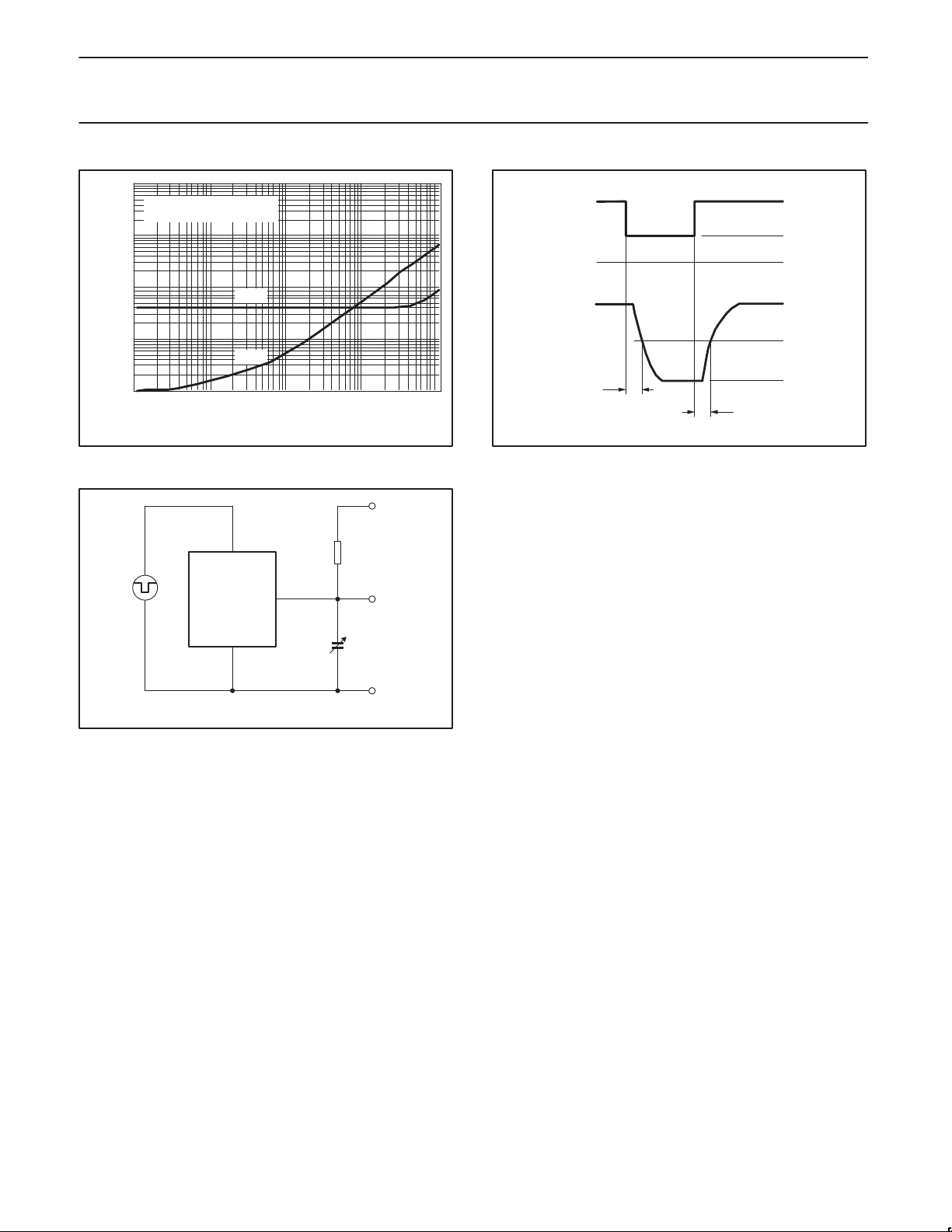
Philips Semiconductors Product data
SA56614-XXCMOS system reset
5
10
T
= 25 °C
AMB
(SEE FIGURES 10 AND 11)
4
10
3
10
, PROPAGATION DELAY ( s)t µ
2
10
PLH
, t
PHL
1
10
–5
10
t
PHL
t
PLH
–4
10
–3
10
10
CL, OUTPUT LOAD CAPACITANCE (µF)
Figure 9. Propagation delay versus output load C.
INPUT SIGNAL
OUTPUT SIGNAL
t
–2
–1
10
PHL
t
PLH
SL01350
Figure 10. Propagation delay measurements.
VS + 2.0 V
1.2 V
V
SS
7.0 V
3.5 V
V
SS
SL01351
V
INPUT
SIGNAL
DD
SA56614-XX
V
SS
RPU = 100 kΩ
C
Figure 11. Propagation delay measurement circuit.
7.0 V
OUTPUT
= 10 pF to 0.1 µF
L
V
SS
SL01352
2001 Jun 19
6
Page 7
Philips Semiconductors Product data
SA56614-XXCMOS system reset
TECHNICAL DESCRIPTION
The SA56614-XX is a CMOS device designed to monitor the
system’s power source and provide a system reset function in the
event the supply voltage sags below an acceptable level for the
system to reliably operate. The SA56614 generates a compatible
reset signal for a wide variety of microprocessor and logic systems.
The device can operate at voltages up to 12 volts. The series
includes several versions providing precision threshold voltage reset
values of 2.0, 2.7, 2.8, 2.9, 3.0, 3.1, 4.2, 4.6, and 4.7 V . The reset
threshold incorporates a typical hysteresis of (V
× 0.05) volts to
S
prevent erratic resets from being generated. The SA56614 operates
at very low supply currents, typically 0.25 µA, while offering a high
precision of threshold detection (±2%).
The output of the SA56614 incorporates an active Totem-Pole
output topology comprised of complimentary P-Channel and
N-Channel FETs. A P-Channel FET is on the high supply side and
when ON pulls the output to or near the V
supply voltage from
DD
which output source current can be obtained. A complimentary
N-Channel FET is on the low or ground side, and actively pulls the
output LOW or to ground with the capability of sinking current into
the output. Both devices supply system reset signals. The user
should keep in mind, when connecting the SA56614 to a system, the
effect of supplying source current from the output of the SA56614 on
the system. This is of particular importance where the SA56614 is
operated from a different supply source than the rest of the system.
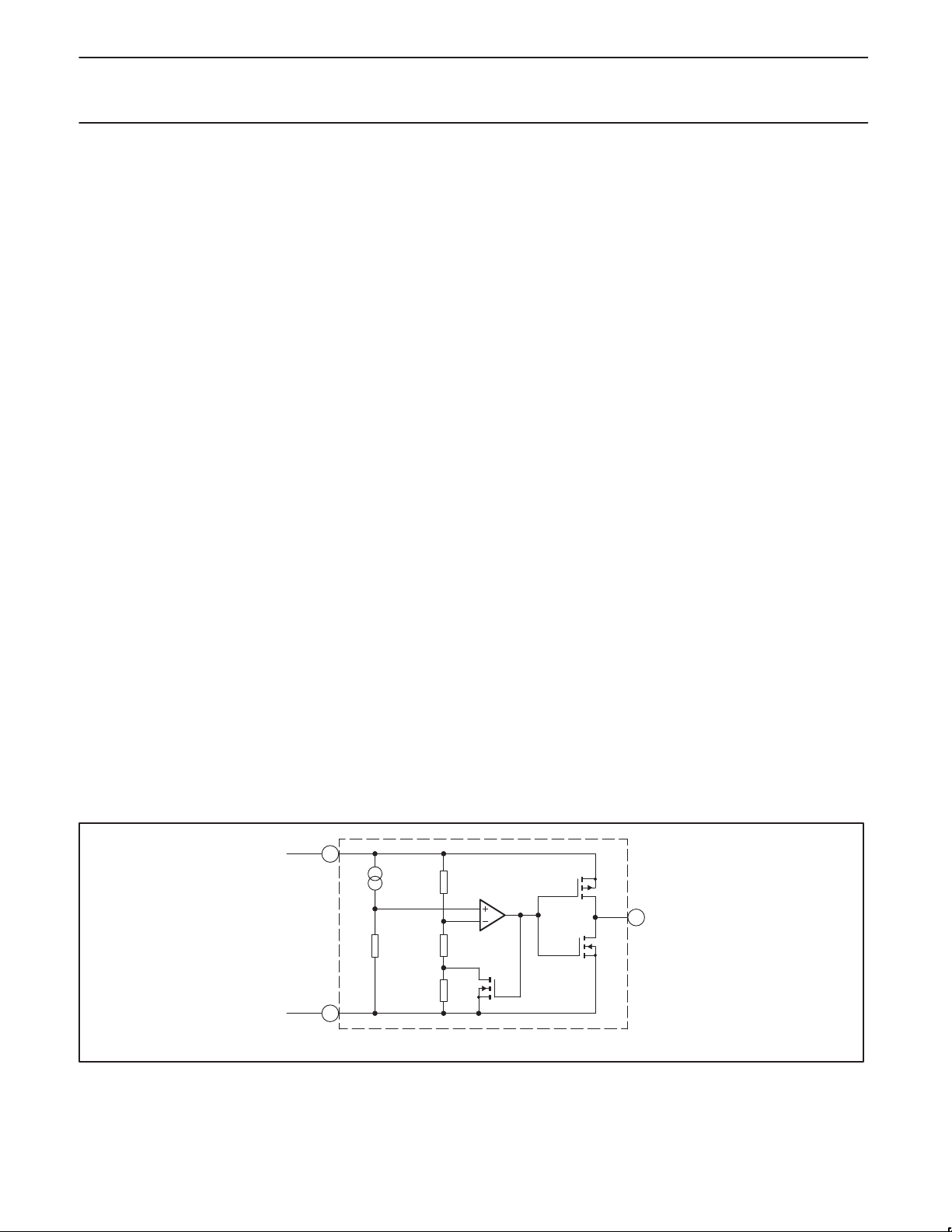
Figure 12 is a functional block diagram of the SA56614. The internal
reference source voltage (V
) is typically 0.8 V over the operating
REF
temperature range. The reference voltage is connected to the
non-inverting input of the threshold comparator while the inverting
input monitors the supply voltage through a resistor divider network
made up of R
, R2, and R3. The output of the threshold comparator
1
drives the totem-pole output stage of the device.
When the supply voltage sags to the threshold detection voltage, the
resistor divider network supplies a voltage to the inverting input of
the threshold comparator which is less than that of V
, causing
REF
the output of the comparator to adopt a HIGH output state. This
causes the high side P-Channel FET of the Totem-Pole output stage
to turn OFF while simultaneously turning the low side N-Channel
FET from OFF to an active ON state, pulling the output to a LOW
voltage state. The device adheres to a true input/output logic
protocol. The output goes to a LOW voltage state when input is
LOW (below V
when the input is HIGH (above V
) and the output HIGH goes to a HIGH voltage state
S
).
S
The low side N-Channel FET (TR3) establishes threshold hysteresis
by turning ON whenever the threshold comparator’s output goes to
a HIGH state (when V
turning ON causes additional current to flow through resistors R
causing the inverting input of the threshold comparator to be
and R
2
sags to or below the threshold level). TR3’s
DD
,
1
pulled even lower. For the comparator to reverse its output polarity
and turn OFF TR
, the VDD source voltage must overcome this
3
additional pull-down voltage present on the comparator’s inverting
input. The differential voltage required to do this establishes the
hysteresis voltage of the sensed threshold voltage. Typically it is
(V
× 0.05) volts.
S
When the VDD voltage sags and is at or below the Detection
Threshold (V
very near ground potential. As the V
< VSL) to VSH or higher, the reset is released and the output
(V
DD
follows V
), the device will assert a Reset LOW output at or
SL
. Conversely, decreases in VDD from (VDD > VSL) to V
DD
voltage rises from
DD
SL
or lower cause the output to be pulled to ground.
Hysteresis Voltage = Release Voltage – Detection Threshold Voltage
V
= VSH – V
HYS
SL
where:
V
= VSL + V
SH
VSL = V
REF(R1
HYS
≅ V
REF(R1
+ R2) / R
+ R2 + R3) / (R2 + R3)
2
When VDD drops below the minimum operating voltage, typically
less than 0.95 volts, the output is undefined and output reset low
assertion is not guaranteed. At this level of V
rise to V
The V
.
DD
voltage is typically 0.8 V . The devices are fabricated using
REF
a high resistance CMOS process and utilize high resistance R
values requiring very small amounts of current. This
and R
3
the output will try to
DD
, R2,
1
combination achieves very efficient low power performance over the
full operating temperature.
2001 Jun 19
V
DD
2
NE56614-XX
R
1
V
REF
R
V
SS
3
R
2
TR
R
3
3
TR
TR
1
2
SL01353
V
OUT
1
Figure 12. Functional diagram
7
Page 8
Philips Semiconductors Product data
SA56614-XXCMOS system reset
TIMING DIAGRAM
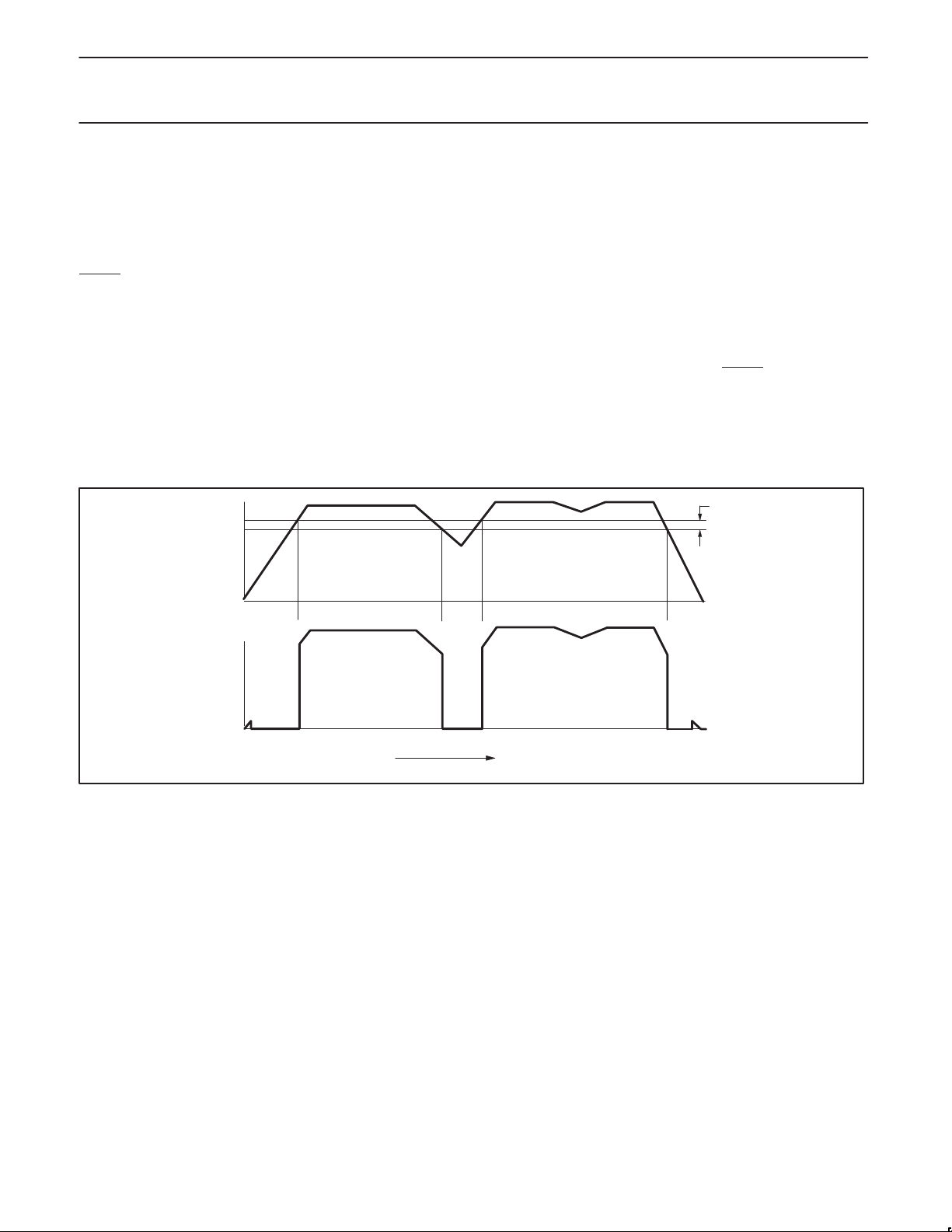
The timing diagram shown in Figure 13 depicts the operation of the
device. Letters A-J on the TIME axis indicate specific events.
A: At ‘A’, V
increases but abruptly decreases when V
begins to increase. Also the V
DD
voltage initially
OUT
reaches the level
DD
(approximately 0.8 V) that activates the internal bias circuitry and
RESET is asserted.
B: At ‘B’, V
device releases the hold on the V
reaches the threshold level of VSH. At this point the
DD
reset. The Reset output V
OUT
OUT
tracks VDD as it rises above VSH (assuming the reset pull-up resistor
R
is connected to VDD). In a microprocessor based system these
PU
events release the reset from the microprocessor, allowing the
microprocessor to function normally.
C-D: At ‘C’, V
begins to fall, causing V
DD
to follow. V
OUT
DD
continues to fall until the VSL undervoltage detection threshold is
reached at ‘D’. This causes a reset signal to be generated (V
OUT
Reset goes LOW).
D-E: Between ‘D’ and ‘E’, V
E: At ‘E’, VDD rises to the VSH. Once again, the device releases
the hold on the V
rises above V
reset. The Reset output V
OUT
.
SH
F-G: At ‘F’, VDD is above the upper threshold and begins to fall,
causing V
to follow it. As long as VDD remains above the VSH,
OUT
no reset signal will be triggered. Before V
begins to rise, causing V
normal.
H: At event ‘H’ V
falls until the VSL undervoltage detection
DD
threshold point is reached. At this level, a RESET
generated and V
goes LOW.
OUT
J: At ‘J’ the VDD voltage has decreased until normal internal circuit
bias is unable to maintain a V
less than 0.8 V. As V
DD
decreases to zero.
starts rising.
DD
OUT
falls to the VSH, it
to follow it. At ‘G’, VDD returns to
OUT
DD
signal is
reset. As a result, VDD may rise to
OUT
decreases further, V
reset also
OUT
tracks VDD as it
V
SH
V
SL
V
DD
0
V
OUT
0
AB C GHJDE F
TIME
Figure 13. Timing diagram.
SL01354
∆V
S
2001 Jun 19
8
Page 9
Philips Semiconductors Product data
SA56614-XXCMOS system reset
APPLICATION INFORMATION
V
GND
DD
V
DD
SA56614-XX
V
SS
CPU
V
OUT
RESET
V
SUPPLY
R
11
R
12
CURRENT CHANGES
A
V
DD
SA56614-XX
V
SS
OUTPUT
SL01355
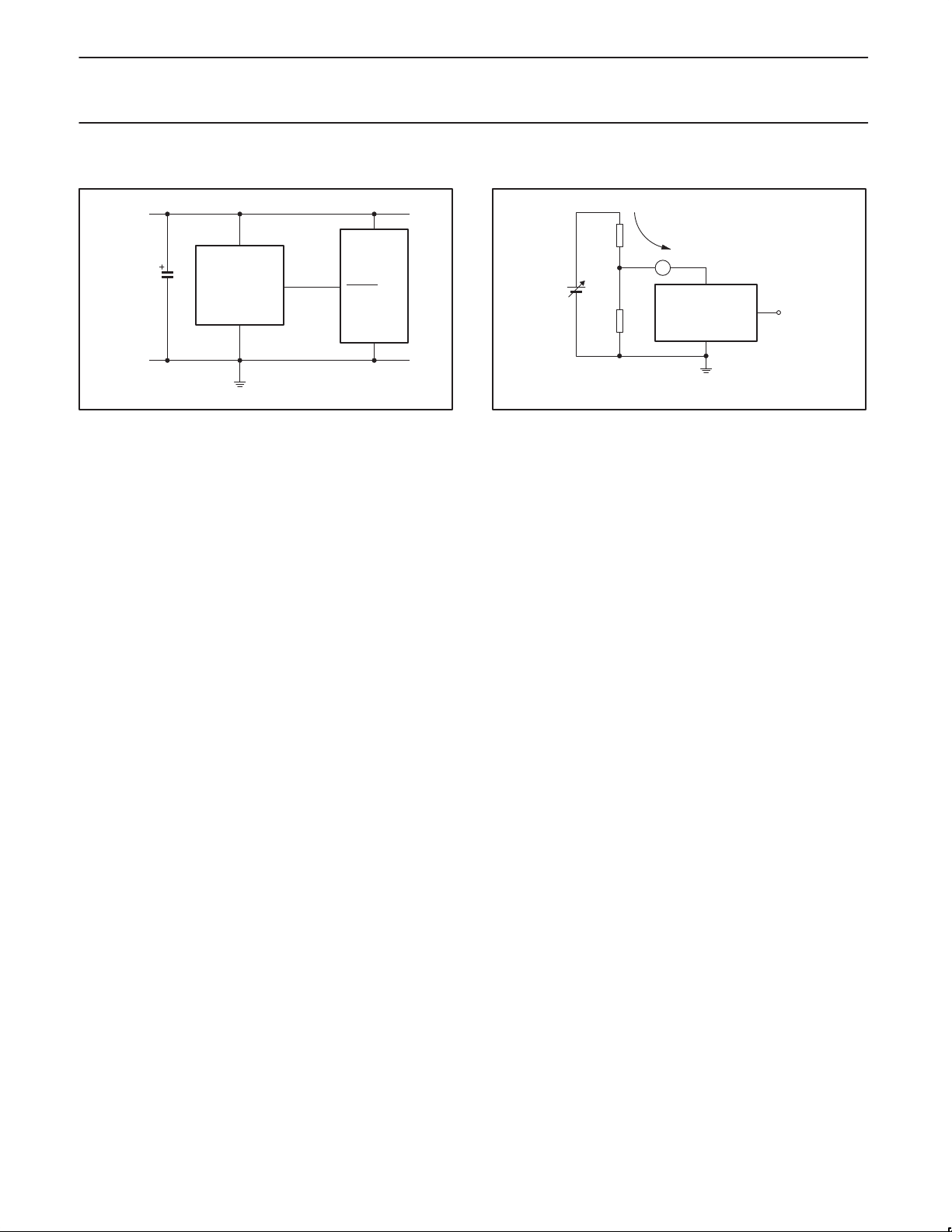
Figure 14. Conventional reset application
Small changes in supply current will occur when the SA56614
asserts or releases a reset. In some cases this can cause
oscillations of the device. This can present a problem, particularly
where high impedance V
sources are employed. Figure 15 shows
DD
how this may occur.
SL01356
Figure 15. High impedance supply operating problems
Significant voltage variations of V
may occur when the device is
DD
operated from high impedance power sources. When the device
asserts or releases a reset, V
of the voltage drop developed across R
variations through the resistor R
impedance). If the V
variations are large, such that they exceed
DD
variations are produced as a result
DD
11
due to the current
11
(representing the supply
the Detection Hysteresis, the output of the device can oscillate from
a HIGH state to a LOW state. The user should avoid using high
impedance V
sources to prevent such situations.
DD
2001 Jun 19
9
Page 10
Philips Semiconductors Product data
SA56614-XXCMOS system reset
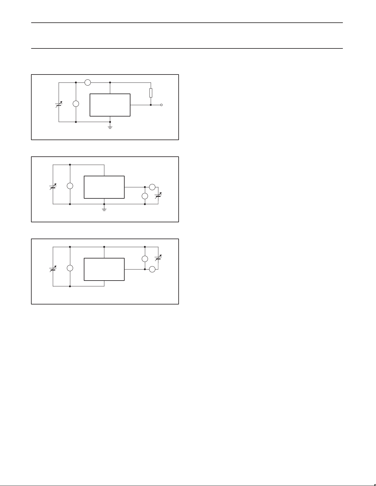
TEST CIRCUITS
A
V
DD
V
DD
V
SA56614-XX
V
SS
V
Figure 16. Test Circuit 1
V
DD
OUT
R
100 kΩ
SL01357
PU
V
DD
V
SA56614-XX
V
SS
V
OUT
A
V
SL01358
V
DS
Figure 17. Test Circuit 2
V
DD
V
DD
V
SA56614-XX
V
SS
V
V
OUT
SL01359
V
DS
A
Figure 18. Test Circuit 3
2001 Jun 19
10
Page 11
Philips Semiconductors Product data
SA56614-XXCMOS system reset
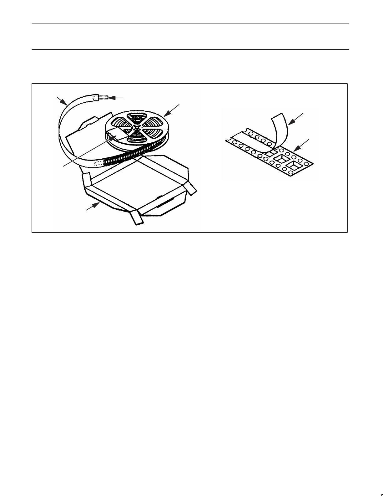
PACKING METHOD
GUARD
BAND
BARCODE
LABEL
BOX
TAPE
REEL
ASSEMBLY
Figure 19. Tape and reel packing method
TAPE DETAIL
COVER TAPE
CARRIER TAPE
SL01305
2001 Jun 19
11
Page 12
Philips Semiconductors Product data
SA56614-XXCMOS system reset
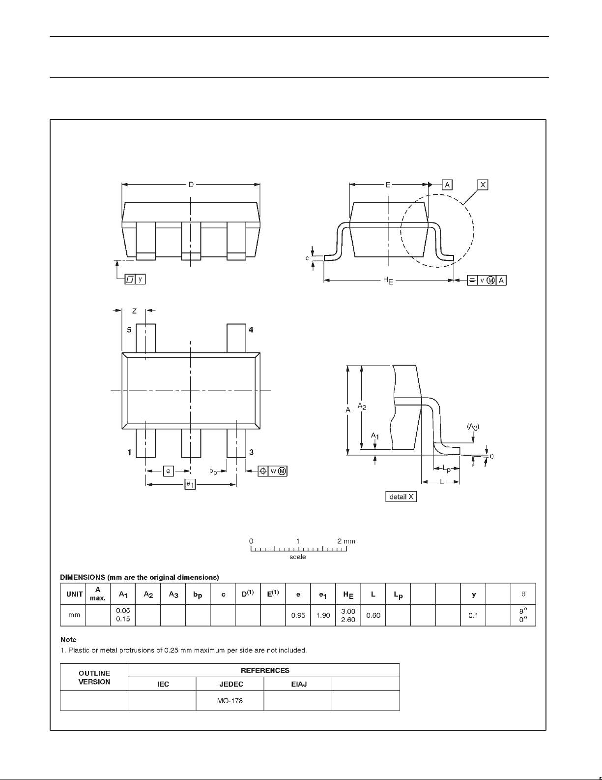
SOT23-5: plastic small outline package; 5 leads; body width 1.5 mm
2001 Jun 19
1.35
1.2
1.0
0.025
0.55
0.41
0.22
0.08
3.00
2.70
1.70
1.50
12
0.55
0.35
Page 13

Philips Semiconductors Product data
SA56614-XXCMOS system reset
NOTES
2001 Jun 19
13
Page 14

Philips Semiconductors Product data
SA56614-XXCMOS system reset
Data sheet status
Product
Data sheet status
Objective data
Preliminary data
Product data
[1] Please consult the most recently issued datasheet before initiating or completing a design.
[2] The product status of the device(s) described in this data sheet may have changed since this data sheet was published. The latest information is available on
the Internet at URL http://www.semiconductors.philips.com.
[1]
status
Development
Qualification
Production
[2]
Definitions
This data sheet contains data from the objective specification for product development.
Philips Semiconductors reserves the right to change the specification in any manner without notice.
This data sheet contains data from the preliminary specification. Supplementary data will be
published at a later date. Philips Semiconductors reserves the right to change the specification
without notice, in order to improve the design and supply the best possible product.
This data sheet contains data from the product specification. Philips Semiconductors reserves the
right to make changes at any time in order to improve the design, manufacturing and supply.
Changes will be communicated according to the Customer Product/Process Change Notification
(CPCN) procedure SNW-SQ-650A.
Definitions
Short-form specification — The data in a short-form specification is extracted from a full data sheet with the same type number and title. For
detailed information see the relevant data sheet or data handbook.
Limiting values definition — Limiting values given are in accordance with the Absolute Maximum Rating System (IEC 134). Stress above one
or more of the limiting values may cause permanent damage to the device. These are stress ratings only and operation of the device at these or
at any other conditions above those given in the Characteristics sections of the specification is not implied. Exposure to limiting values for extended
periods may affect device reliability.
Application information — Applications that are described herein for any of these products are for illustrative purposes only. Philips
Semiconductors make no representation or warranty that such applications will be suitable for the specified use without further testing or
modification.
Disclaimers
Life support — These products are not designed for use in life support appliances, devices or systems where malfunction of these products can
reasonably be expected to result in personal injury . Philips Semiconductors customers using or selling these products for use in such applications
do so at their own risk and agree to fully indemnify Philips Semiconductors for any damages resulting from such application.
Right to make changes — Philips Semiconductors reserves the right to make changes, without notice, in the products, including circuits, standard
cells, and/or software, described or contained herein in order to improve design and/or performance. Philips Semiconductors assumes no
responsibility or liability for the use of any of these products, conveys no license or title under any patent, copyright, or mask work right to these
products, and makes no representations or warranties that these products are free from patent, copyright, or mask work right infringement, unless
otherwise specified.
Philips Semiconductors
811 East Arques Avenue
P.O. Box 3409
Sunnyvale, California 94088–3409
Telephone 800-234-7381
Copyright Philips Electronics North America Corporation 2001
All rights reserved. Printed in U.S.A.
Date of release: 06-01
Document order number: 9397 750 08453
2001 Jun 19
14
 Loading...