

Philips SA5225D Datasheet

INTEGRATED CIRCUITS
SA5225
Fiber optic postamplifier
Product specification
Replaces datasheet NE/SA5225 of 1997 Jun 05
IC19 Data Handbook
1998 Oct 07
Philips Semiconductors Product specification
SA5225Fiber optic postamplifier
DESCRIPTION
The SA5225 is a high-gain limiting amplifier that is designed to
process signals from fiber optic preamplifiers. Capable of operating
at 125Mb/s, the chip has input signal level-detection with a
user-adjustable threshold. The DATA and LEVEL-DETECT outputs
are differential for optimum noise margin and ease of use. Also
available is the SA5224 which is optimized for FDDI applications.
FEA TURES
•Wideband operation: 1.0kHz to 120MHz typical
•Applicable in 155Mb/s OC3/SONET receivers
•Operation with single +5V or –5.2V supply
•Differential 10k ECL outputs
•Programmable input signal level-detection
•Fully differential for excellent PSRR to 1GHz
APPLICATIONS
•Data communication in noisy industrial environments
•LANs
ORDERING INFORMATION
DESCRIPTION TEMPERATURE RANGE ORDER CODE DWG #
16-Pin Plastic Small Outline (SO) Package
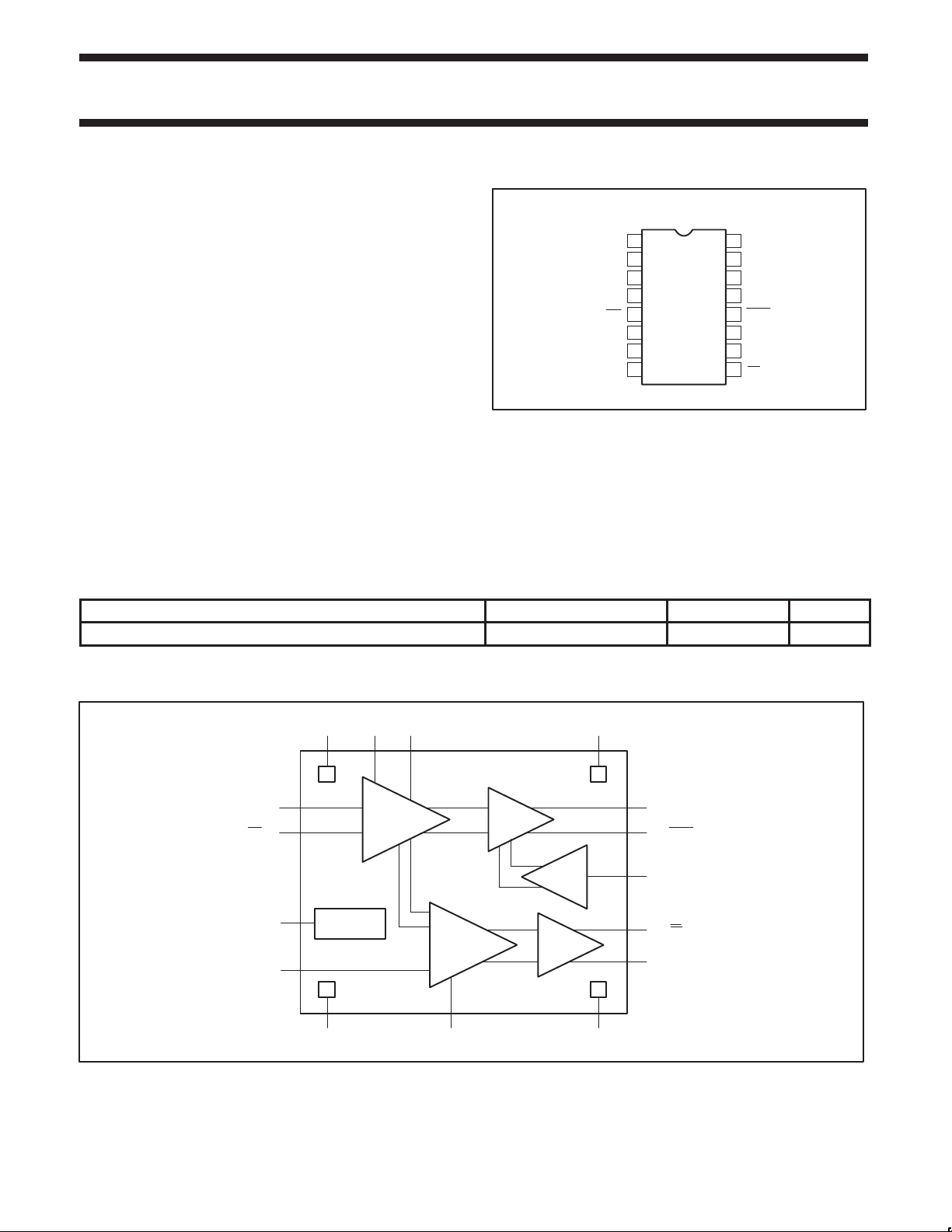
PIN DESCRIPTION
CAZN
CAZP
GND
D
IN
D
IN
V
CCA
CF
JAM
Figure 1. Pin Configuration
–40 to +85°C
A
D Package
1
2
3
4
5
6
7
8
16
V
SET
V
15
REF
14
V
CCE
13
D
OUT
12
D
OUT
11
GND
E
ST
10
9
ST
SD00374
SA5225D SOT109-1
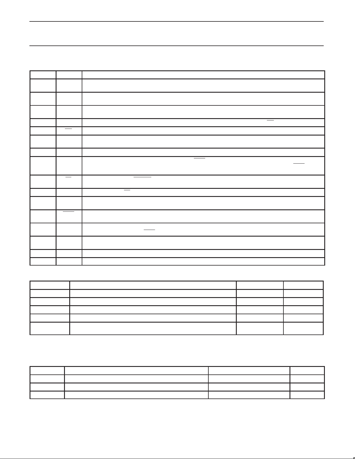
BLOCK DIAGRAM
V
V
D
D
REF
SET
C
V
(4)
IN
(5)
IN
(15)
(16)
GND
C
AZN
A
AZP
LIMITING
AMPLIFIER
LEVEL
DETECTOR
C
F
ECL
BUFFER
CCA
(6) (2) (1) (16)
REFERENCE
JAM
BUFFER
SD
BUFFER
V
CCE
(11)(7)(3)
GND
(13)
D
OUT
(12)
D
OUT
JAM
(8)
ST
(9)
(10)
ST
SD00375
E
Figure 2. Block Diagram
1998 Oct 07 853-1595 20141
2
Philips Semiconductors Product specification
SA5225Fiber optic postamplifier
PIN DESCRIPTIONS
PIN NO. NAME FUNCTION
1 C
2 C
AZN
AZP
3 GNDAAnalog GND pin. Connect to ground for +5V upshifted ECL operation. Connect to –5.2V for standard ECL
4 D
5 D
6 V
CCA
7 C
8 JAM This ECL-compatible input controls the output buffers D
9 ST Input signal level-detect STATUS. This ECL output is high when the input signal is below the user programmable
10 ST ECL compliment of ST (Pin 9).
11 GND
12 D
13 D
14 V
15 V
16 V
OUT
OUT
CCE
REF
SET
Auto-zero capacitor pin. Connecting a capacitor between this pin and C
limiting amplifier.
Auto-zero capacitor pin. Connecting a capacitor between this pin and C
limiting amplifier.
will cancel the offset voltage of the
AZP
will cancel the offset voltage of the
AZN
operation. Must be at same potential as GNDE (Pin 11).
Differential input. DC bias level is set internally at approximately 2.9V. Complimentary to DIN (Pin 5).
IN
Differential input. DC bias level is set internally at approximately 2.9V. Complimentary to DIN (Pin 4).
IN
Analog power supply pin. Connect to a +5V supply for upshifted ECL operation. Connect to ground for standard
ECL operation. Must be at same potential as V
Filter capacitor for level detector. Capacitor should be connected between this pin and V
F
is applied, the outputs will follow the input signal. When an ECL HIGH signal is applied, the D
will latch into LOW and HIGH states, respectively. When left unconnected, this pin is actively pulled-low (JAM OFF).
CCE
(Pin 14).
OUT
and D
.
CCA
(Pins 12 and 13). When an ECL LOW signal
OUT
OUT
and D
threshold level.
Digital GND pin. Connect to ground for +5V upshifted ECL operation. Connect to a negative supply for normal ECL
E
operation. Must be at the same potential as GNDA (Pin 3).
ECL-compatible output. Nominal level is V
condition. Complimentary to D
OUT
(Pin 13).
ECL-compatible output. Nominal level is V
condition. Complimentary to D
OUT
(Pin 12).
–1.3V. When JAM is HIGH, this pin will be forced into an ECL HIGH
CCE
–1.3V. When JAM is HIGH, this pin will be forced into an ECL LOW
CCE
Digital power supply pin. Connect to a +5V supply for upshifted ECL operation. Connect to ground during normal
ECL operation. Must be at the same potential as V
CCA
(Pin 6).
Reference voltage for threshold level voltage divider. Nominal value is approximately 2.64V.
Input threshold level setting circuit. This input can come from a voltage divider between V
and GNDA.
REF
OUT
pins
ABSOLUTE MAXIMUM RATINGS
SYMBOL PARAMETER RATING UNITS
T
V
P
CC
T
A
T
J
STG
D
Power supply (VCC - GND) 6 V
Operating ambient –40 to +85 °C
Operating junction –55 to +150 °C
Storage –65 to +150 °C
Power dissipation, TA = 25°C (still air)
16-pin Plastic SO
1
1100 mW
NOTE:
1. Maximum dissipation is determined by the ambient temperature and the thermal resistance,
: 16-pin SO: θJA = 110°C/W
θ
JA
RECOMMENDED OPERATING CONDITIONS
SYMBOL PARAMETER RATING UNITS
V
CC
T
A
T
J
Supply voltage 4.5 to 5.5 V
Ambient temperature ranges –40 to +85 °C
Junction temperature ranges –40 to +110 °C
1998 Oct 07
3
 Loading...