

Philips sa5222 DATASHEETS
Philips Semiconductors Product specification
SA5222Low-power FDDI transimpedance amplifier
1
1995 Apr 26 853-1582 15170
DESCRIPTION
The NE/SA5222 is a low-power, wide-band, low noise
transimpedance amplifier with differential outputs, optimized for
signal recovery in FDDI fiber optic receivers. The part is also suited
for many other RF and fiber optic applications as a general purpose
gain block.
FEATURES
•Extremely low noise:
z
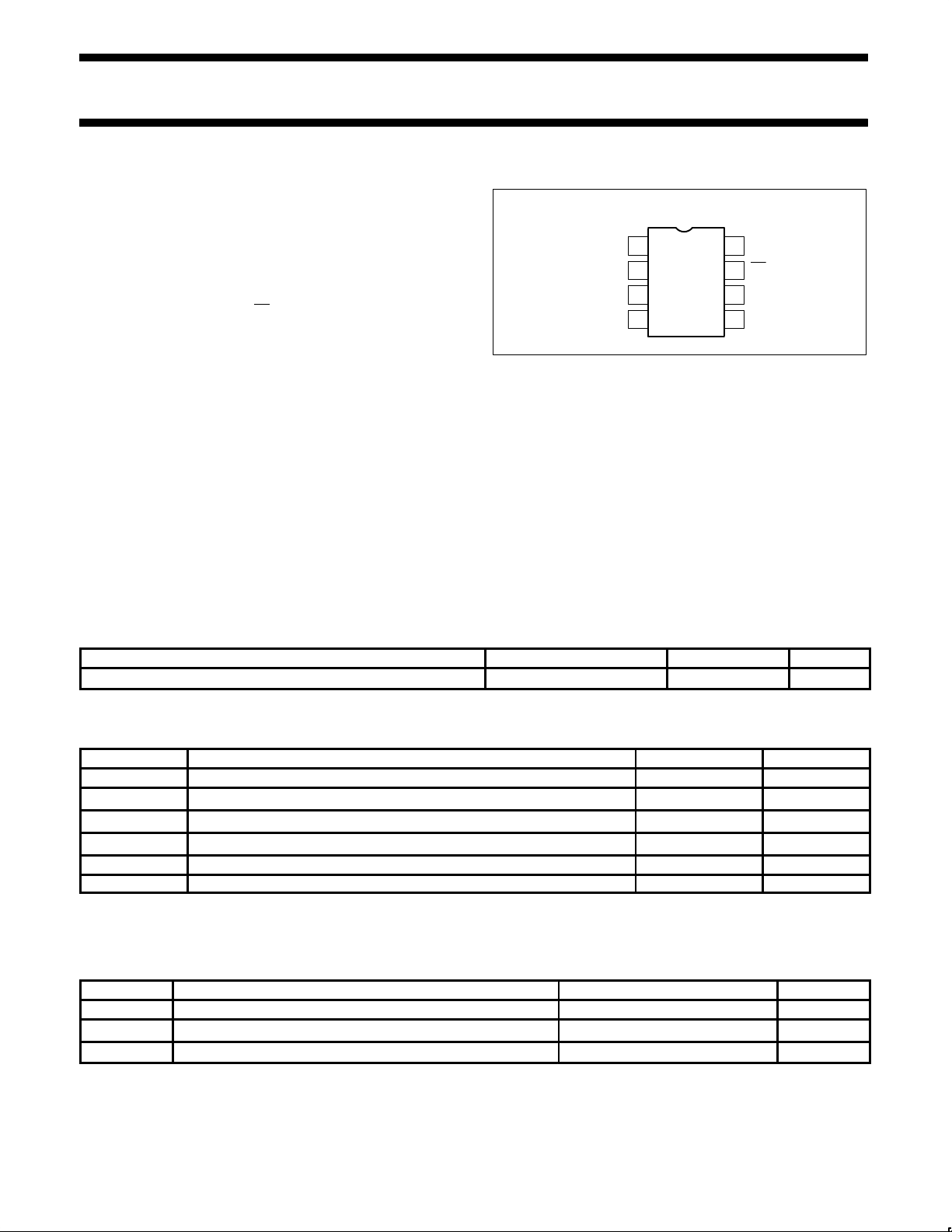
D Package
IN
GND
2
OUT
V
CC2
1
2
3
4
8
7
6
5
OUT
GND
1
V
CC1
GND
1
SD00360
Figure 1. Pin Configuration
APPLICATIONS
•FDDI preamp
•Current-to-voltage converters
•Wide-band gain block
•Medical and scientific instrumentation
•Sensor preamplifiers
•Single-ended to differential conversion
•Low noise RF amplifiers
•RF signal processing
ORDERING INFORMATION
DESCRIPTION TEMPERATURE RANGE ORDER CODE DWG #
8-Pin Plastic Small Outline (SO) package
-40 to +85°C
SA5222D SOT96-1
ABSOLUTE MAXIMUM RATINGS
SYMBOL PARAMETER RATING UNITS
V
CC1,2
Power supply voltage 6 V
T
A
Ambient temperature range -40 to +85
°C
T
J
Junction temperature range -55 to +150
°C
T
STG
Storage temperature range -65 to +150
°C
P
D
Power dissipation TA = 25oC (still air)
1
0.78 W
I
INMAX
Maximum input current 5 mA
NOTE:
1. Maximum power dissipation is determined by the operating ambient temperature and the thermal resistance θJA = 158oC/W. Derate
6.2mW/
°C above 25°C.
RECOMMENDED OPERATING CONDITIONS
SYMBOL PARAMETER RATING UNITS
V
CC1,2
Power supply voltage 4.5 to 5.5 V
T
A
Ambient temperature range: SA grade -40 to +85
°C
T
J
Junction temperature range: SA grade -40 to +105
°C
2.0pAH
•Single 5V supply
•Low supply current: 9mA
•Large bandwidth: 165MHz
•Differential outputs
•Low output offset
•Low input/output impedances
•High power-supply-rejection ratio: 55dB
•Tight transresistance control
•High input overload: 115µA
•ESD protected
PIN DESCRIPTION
Philips Semiconductors Product specification
SA5222Low-power FDDI transimpedance amplifier
1995 Apr 26
2
DC ELECTRICAL CHARACTERISTICS
Typical data and Min and Max limits apply at TA = 25°C, and V
CC1
= V
CC2
= +5V, unless otherwise specified.
SA5222
SYMBOL
PARAMETER
TEST CONDITIONS
Min Typ Max
UNIT
V
IN
Input bias voltage 1.3 1.55 1.8 V
V
O
±
Output bias voltage 2.9 3.2 3.5 V
V
OS
Output offset voltage 0 ±100 mV
I
CC
Supply current 6 9 12 mA
I
OMAX
Output sink/source current 1.5 2 mA
I
IN
Input current (2% linearity) Test circuit 5, Procedure 2 ±60 ±90
µA
I
INMAX
Maximum input current overload threshold Test circuit 5, Procedure 4 ±80 ±115
µA
V
OMAX
Maximum differential output voltage swing R
L
= ∞, Test Circuit 5, Procedure 3 3.6 V
P-P
AC ELECTRICAL CHARACTERISTICS
Typical data and Min and Max limits apply at TA = 25°C and V
CC1
= V
CC2
=+5V, unless otherwise specified.
SA5222
SYMBOL
PARAMETER
TEST CONDITIONS
Min Typ Max
UNIT
R
T
Transresistance (differential output)
DC tested, RL = ∞, Test Circuit 5,
Procedure 1
13.3 16.6 19.9 kΩ
R
O
Output resistance
(differential output)
DC tested 30 60 90 Ω
R
T
Transresistance
(single-ended output)
DC tested, RL = ∞
6.65 8.3 9.95 kΩ
R
O
Output resistance
(single-ended output)
DC tested 15 30 45 Ω
f
3dB
Bandwidth (-3dB)
1
Test Circuit 1 110 140 MHz
R
IN
Input resistance 150
Ω
C
IN
Input capacitance
2
1
pF
∆R/∆V Transresistance power supply sensitivity V
CC1
= V
CC2
= 5 ±0.5V 1.0 %/V
∆R/∆T
Transresistance ambient temperature sensitivity
∆TA = T
A MAX
- T
A MIN
0.07
%/oC
I
IN
RMS noise current spectral density (referred
to input)
Test Circuit 2, f = 10MHz 2.0
p
Integrated RMS noise current over the bandwidth (referred to input)
Test circuit 2,
∆f = 50MHz
15
CS = 0pF ∆f = 100MHz 25
∆f = 150MHz 36
I
T
CS = 1pF ∆f = 50MHz 17
nA
∆f = 100MHz 35
∆f = 150MHz 55
PSRR Power supply rejection ratio DC Tested, ∆VCC = ±0.5V –55 dB
PSRR Power supply rejection ratio
3
f = 1.0MHz, Test Circuit 3 –34 dB
I
INMAX
Maximum input amplitude for output duty
cycle of 50 ±5%
4
Test circuit 4 ±120 µA
tr, tfRise and fall times 10 – 90% 2.2 ns
t
D
Group delay f = 10MHz 2.2 ns
NOTES:
1. Bandwidth is tested into 50Ω load. Bandwidth into 1kΩ load is approximately 165MHz.
2. Does not include Miller-multiplied capacitance of input device.
3. PSRR is output referenced and is circuit board layout dependent at higher frequencies. For best performance use a RF filter in V
CC
line.
4. Monitored in production via linearity and over load tests.
I
T
A Hz
nA
Philips Semiconductors Product specification
SA5222Low-power FDDI transimpedance amplifier
1995 Apr 26
3
TEST CIRCUITS
Test Circuit 1: Bandwidth
NETWORK ANALYZER
S-PARAMETER TEST SET
PORT1 PORT2
V
CC
20
.1uF
20
.1uF
50
Z
O
= 50Ω
OUT
OUT
IN DUT
0.1uF
R=1k
50
GND
1
SINGLE-ENDED
DIFFERENTIAL
RO = Z
O
1 + S22
1 - S22
-20
RO = 2Z
O
1 + S22
1 - S22
-40
GND
2
RT+
V
OUT
V
IN
R + 4 @ S21@ RRT+
V
OUT
V
IN
R + 2 @ S21@ R
Z
O
= 50Ω
SD00361
Figure 2. Test Circuit1
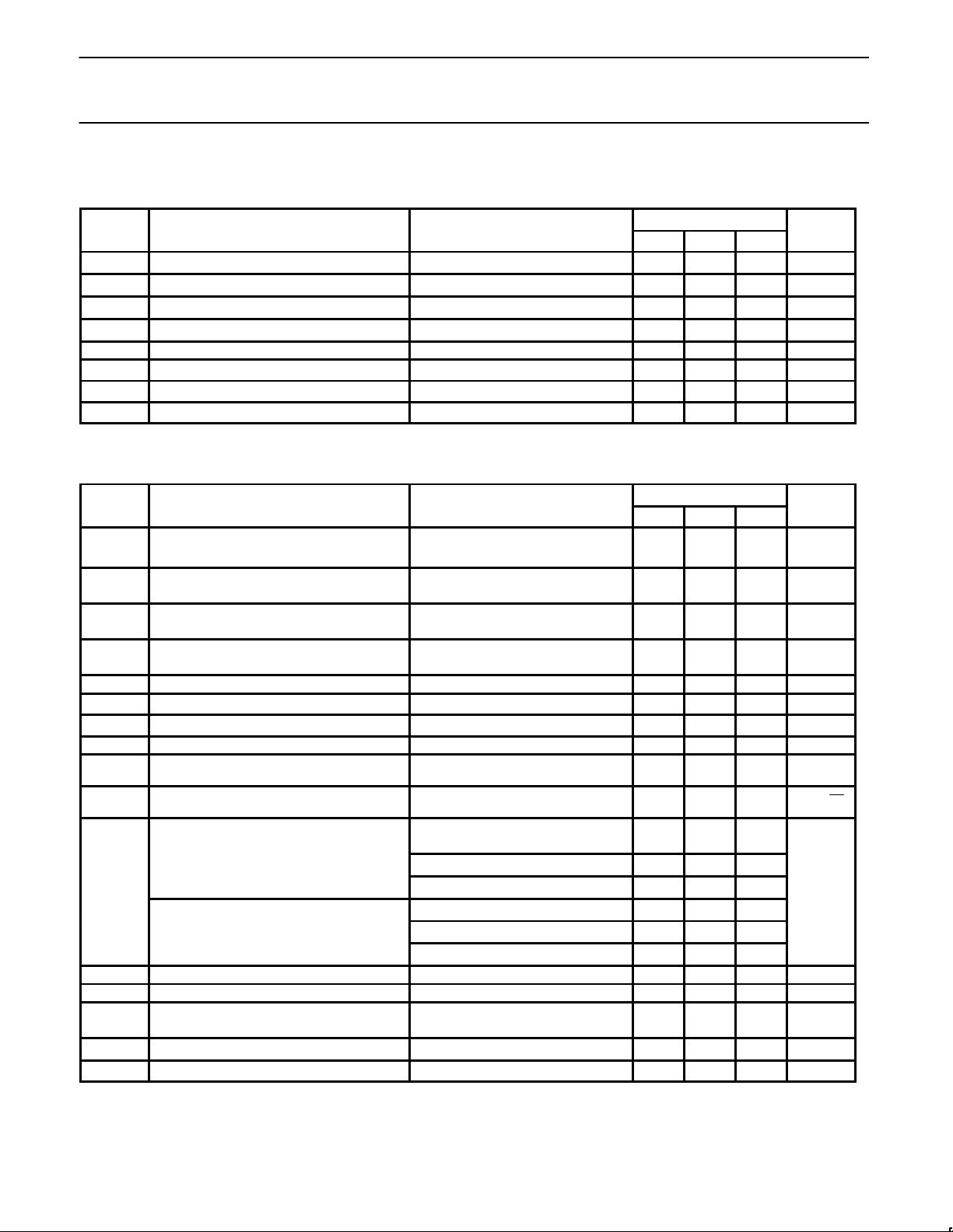
Test Circuit 2: Noise
SPECTRUM ANALYZER
V
CC
20
20
OUT
OUT
IN DUT
GND
2
GND
1
NE5209
50Ω
.1µF
.1µF
10µF
10µF
C
S
50Ω
SD00362
Figure 3. Test Circuit2
TEST CIRCUITS (continued)
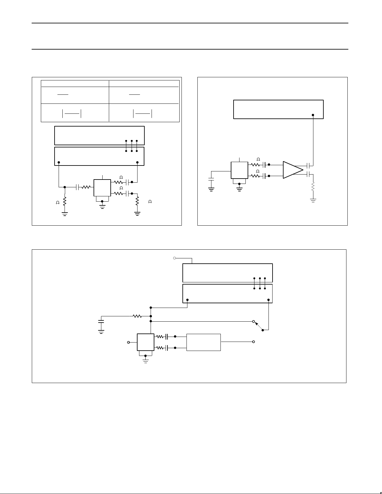
Test Circuit 3: PSRR
NETWORK ANALYZER
S-PARAMETER TEST SET
PORT1 PORT2
V
CC
20Ω
.1uF
20Ω
.1uF
OUT
OUT
IN DUT
GND
2
GND
1
50Ω
CAL
UNBAL.
0.1uF
NC
50Ω
BIAS TEE
5V
NHO300HB
TRANSFORMER
CONVERSION
LOSS = 9dB
100Ω
BAL.
SD00363
Figure 4. Test Circuit4
 Loading...