

Philips SA5217D Datasheet

INTEGRATED CIRCUITS
SA5217
Postamplifier with link status indicator
Product specification
Replaces datasheet NE/SA5217 of 1995 Apr 26
IC19 Data Handbook
1998 Oct 07
Philips Semiconductors Product specification
SA5217Postamplifier with link status indicator
DESCRIPTION
The SA5217 is a 75MHz postamplifier system designed to accept
low level high-speed signals. These signals are converted into a
TTL level at the output. The SA5217 can be DC coupled with the
previous transimpedance stage using SA5210, SA5211 or SA5212A
transimpedance amplifiers. The main difference between the
SA5217 and the SA5214 is that the SA5217 does not make the
output of A1 and input of A2 accessible; instead, it brings out the
output of A2 and the input of A8 thus activating the on-chip Schmitt
trigger function by connecting two external capacitors. The result is
that a much longer string of 1s and 0s, in the bit stream, can be
tolerated. This ”system on a chip” features an auto-zeroed first
stage with noise shaping, a symmetrical limiting second stage, and a
matched rise/fall time TTL output buffer. The system is
user-configurable to provide adjustable input threshold and
hysteresis. The threshold capability allows the user to maximize
signal-to-noise ratio, thereby insuring a low Bit Error Rate (BER).
An auto-zero loop can be used to replace two input coupling
capacitors with a single Auto Zero (AZ) capacitor. A signal absent
flag indicates when signals are below threshold. The low signal
condition forces the TTL output to the last logic state. User
interaction with this ”jamming” system is available. The SA5217 is
packaged in a standard 20-pin surface-mount package and typically
consumes 40mA from a standard 5V supply. The SA5217 is
designed as a companion to the SA5211/5212A and SA5210
transimpedance amplifiers. These differential preamplifiers may be
directly coupled to the postamplifier inputs. The SA5210/5217,
SA5211/5217 or SA5212A/5217 combinations convert nanoamps of
photodetector current into standard digital TTL levels.
APPLICATIONS
•Fiber optics
•Communication links in Industrial and/or Telecom environment
with high EMI/RFI
•Local Area Networks (LAN)
•Synchronous Optical Networks (SONET) STS-1
•RF limiter
•Good for 2
23
-1 pseudo random bit stream
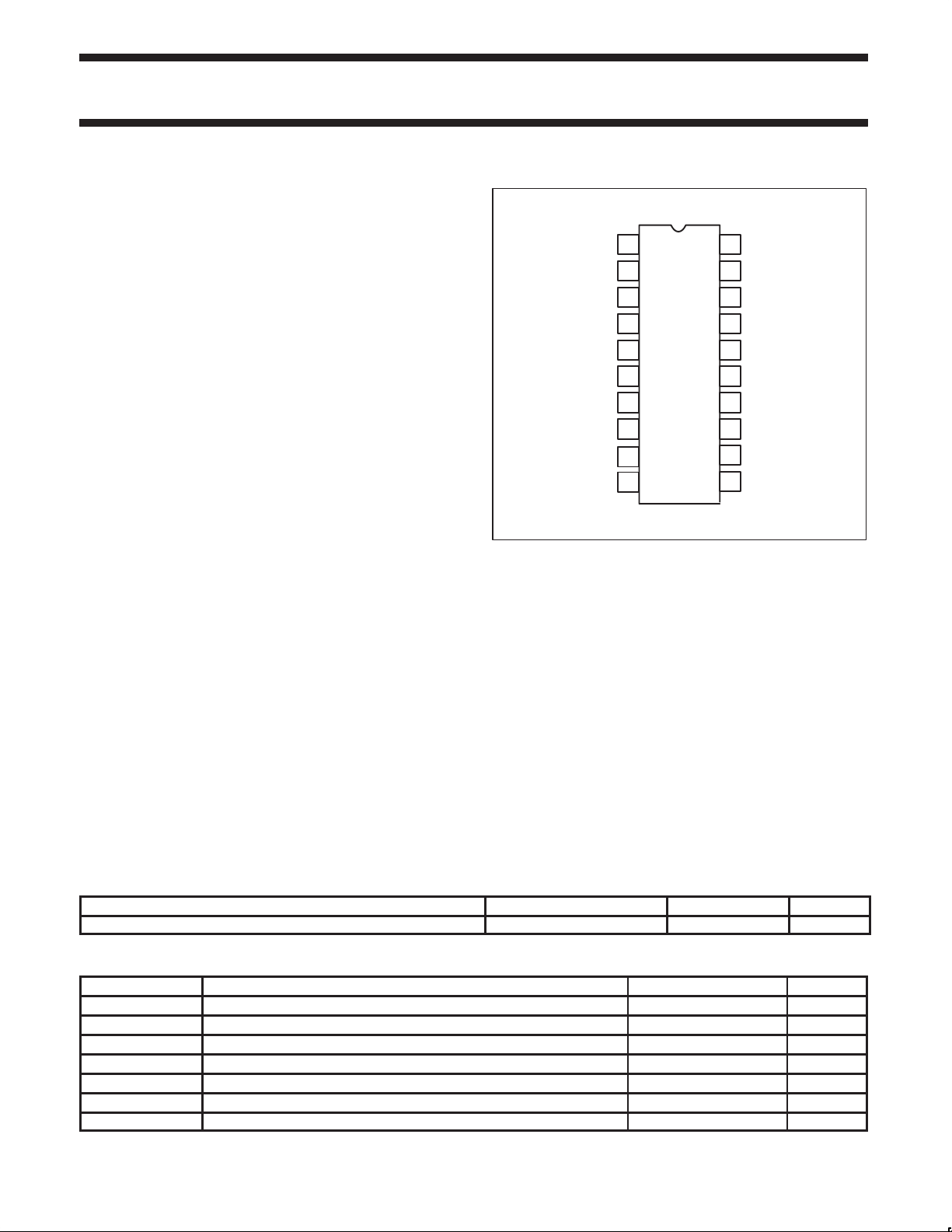
PIN CONFIGURATION
D1 Package
LED
1
GND
FLAG
JAM
V
CCD
V
CCA
GND
V
OUT
2
3
4
A
5
6
7
8
9
D
10
C
PKDET
THRESH
NOTE:
1. SOL - Released in large SO package only.
20
19
18
17
16
15
14
13
12
11
IN
1B
IN
1A
C
AZP
C
AZN
OUT
2B
IN
8B
OUT
2A
IN
8A
R
HYST
R
PKDET
SD00354
Figure 1. Pin Configuration
FEATURES
•Postamp for the SA5211/5212A. SA5210 preamplifier family
•Wideband operation: typical 75MHz (150MBaud NRZ)
•Interstage filtering/equalization possible
•Single 5V supply
•Low signal flag
•Output disable
•Link status threshold and hysteresis programmable
•LED driver (normally ON with above threshold signal)
•Fully differential for excellent PSRR
•Auto-zero loop for DC offset cancellation
•2kV ElectroStatic Discharge (ESD) protection
ORDERING INFORMATION
DESCRIPTION TEMPERATURE RANGE ORDER CODE DWG #
20-Pin Plastic Small Outline Large (SOL) Package -40 to +85°C SA5217D SOT163-1
ABSOLUTE MAXIMUM RATINGS
SYMBOL PARAMETER SA5214 UNIT
V
CCA
V
CCD
T
A
T
J
T
STG
P
D
V
IJ
1998 Oct 07 853-1658 20141
Power supply +6 V
Power supply +6 V
Operating ambient temperature range -40 to +85 °C
Operating junction temperature range -55 to +150 °C
Storage temperature range -65 to +150 °C
Power dissipation 1.4 W
Jam input voltage -0.5 to 5.5 V
2
Philips Semiconductors Product specification
SA5217Postamplifier with link status indicator
PIN DESCRIPTIONS
PIN
SYMBOL DESCRIPTION
NO.
1 LED Output for the LED driver. Open collector output transistor with 125Ω series limiting resistor. An above threshold signal
turns this transistor ON.
2 C
PKDET
3 THRESH Peak detector threshold resistor. The value of this resistor determines the threshold level of the peak detector.
4 GND
5 FLAG Peak detector digital output. When this output is LOW, there is data present above the threshold. This pin is normally
6 JAM Input to inhibit data flow. Sending the pin HIGH forces TTL DATA OUT ON, Pin 10, LOW. This pin is normally connected
7 V
CCD
8 V
CCA
9 GND
10 V
OUT
11 R
PKDET
12 R
HYST
13 IN
8A
14 OUT
15 IN
8B
16 OUT
17 C
AZN
18 C
AZP
19 IN
1A
20 IN
1B
Capacitor for the peak detector. The value of this capacitor determines the detector response time to the signal, supplementing the internal 10pF capacitor.
Device analog ground pin.
A
connected to the JAM pin and has a TTL fanout of two.
to the FLAG pin and is TTL-compatible.
Power supply pin for the digital portion of the chip.
Power supply pin for the analog portion of the chip.
Device digital ground pin.
D
TTL output pin with a fanout of five.
Peak detector current resistor. The value of this resistor determines the amount of discharge current available to the
peak detector capacitor, C
PKDET
.
Peak detector hysteresis resistor. The value of this resistor determines the amount of hysteresis in the peak detector.
Non-inverting input to amplifier A8.
Non-inverting output of amplifier A2.
2A
Inverting input to amplifier A8.
Inverting output of amplifier A2.
2B
Auto-Zero capacitor pin (Negative terminal). The value of this capacitor determines the low-end frequency response of
the preamp A1.
Auto-Zero capacitor pin (Positive terminal). The value of this capacitor determines the low-end frequency response of the
preamp A1.
Non-inverting input of the preamp A1.
Inverting input of the preamp A1.
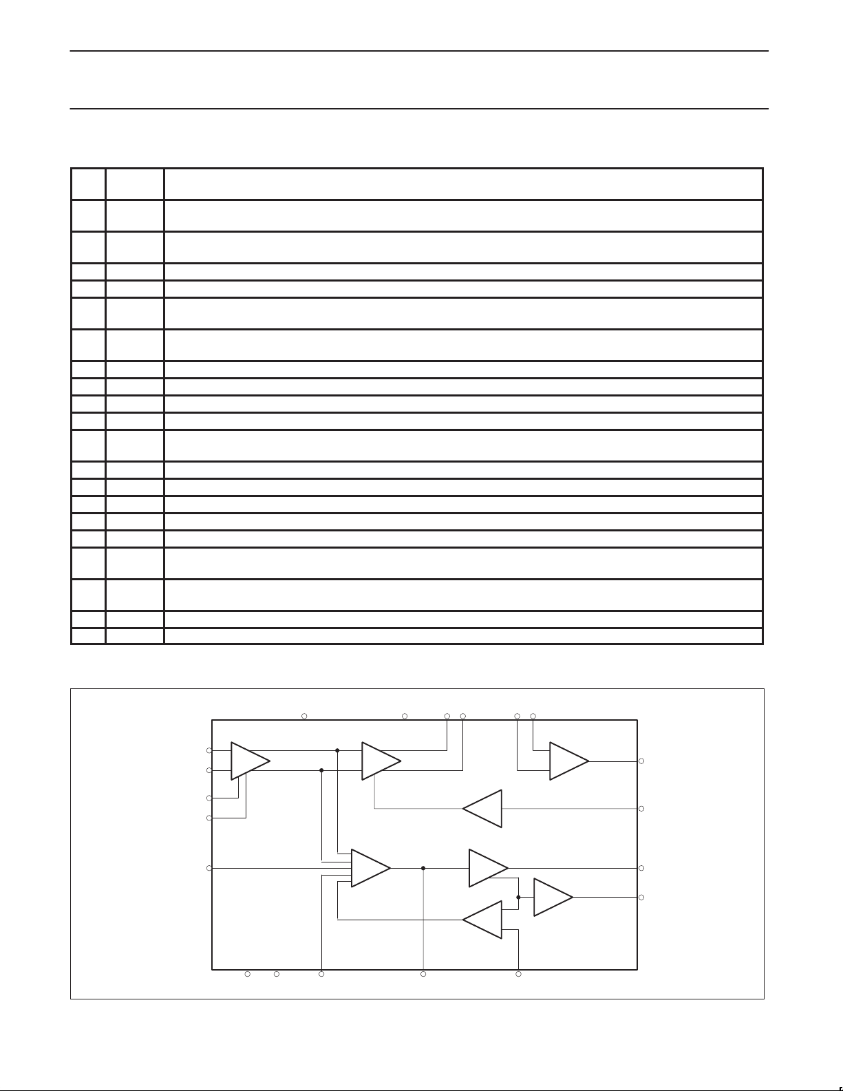
BLOCK DIAGRAM
R
PKDET
1998 Oct 07
C
C
IN
IN
AZP
AZN
1B
1A
V
CCA
87
20
A1 A2
19
18
17
11
9
43
GNDAGND
THRESH
D
V
OUT2AOUT
CCD
GATED AMP
PEAK DETECT
A3
2
C
PKDET
Figure 2. Block Diagram
3
2B
161514
A6
A4
A7
HYSTERESIS
IN8BIN
8A
13
SCHMITT TRIGGER
A8
OUTPUT DISABLE
A5
LED DRIVER
12
R
HYST
10
6
5
1
SD00355
V
OUT
JAM
FLAG
LED
Philips Semiconductors Product specification
SYMBOL
PARAMETER
TEST CONDITIONS
UNIT
SA5217Postamplifier with link status indicator
RECOMMENDED OPERATING CONDITIONS
SYMBOL PARAMETER RATING UNIT
V
CCA
V
CCD
T
A
T
J
P
D
DC ELECTRICAL CHARACTERISTICS
Min and Max limits apply over the operating temperature range at V
= V
CCA
CCD
V
I1
V
O2
I8L
I8H
OH
OL
I
OH
I
OL
I
OS
IHJ
ILJ
I
IHJ
I
ILJ
OHF
OLF
OHF
OLF
SCF
= +5.0V and T
CCD
V
CCA
V
THRESH
V
RPKDET
V
I
I
V
V
V
V
RHYST
V
V
V
V
I
I
I
I
LEDH
Power supply 4.5 to 5.5 V
Power supply 4.5 to 5.5 V
Ambient temperature range -40 to +85 °C
Operating junction temperature range -40 to +110 °C
Power dissipation 300 mW
= V
= +5.0V unless otherwise specified. Typical data applies at
CCD
= 25°C.
A
CCA
LIMITS
Min Typ Max
Analog supply current 30 41.2 mA
Digital supply current (TTL, Flag, LED) 10 13.5 mA
A1 input bias voltage (A,B inputs) 3.08 3.4 3.70 V
A1 output bias voltage (A,B outputs) 3.10 3.8 4.50 V
A8 input bias voltage Low (A,B inputs) 3.40 3.55 3.68 V
A8 input bias voltage High (A,B inputs) 3.68 3.91 4.12 V
High-level TTL output voltage IOH=-200µA 2.4 3.4 V
Low-level TTL output voltage IOL=8mA 0.3 0.4 V
High-level TTL output current V
Low-level TTL output current V
Short-circuit TTL output current V
=2.4V -40 -24.4 mA
OUT
=0.4V 7.0 30 mA
OUT
=0.0V -95 mA
OUT
Threshold bias voltage Pin 3 Open 0.75 V
RPKDET Pin 11 Open 0.72 V
RHYST bias voltage Pin 12 Open 0.72 V
High-level jam input voltage 2.0 V
Low-level jam input voltage 0.8 V
High-level jam input current VIJ=2.7V 30 µA
Low-level jam input current VIJ=0.4V -485 -240 µA
High-level flag output voltage IOH=-80µA 2.4 3.8 V
Low-level flag output voltage IOL=3.2mA 0.33 0.4 V
High-level flag output current V
Low-level flag output current V
Short-circuit flag output current V
LED ON maximum sink current V
=2.4V -18 -5 mA
OUT
=0.4V 3.25 10 mA
OUT
=0.0V -61 -40 -26 mA
OUT
=3.0V 8 22 80 mA
LED
1998 Oct 07
4
 Loading...