

Philips SA5212AD, SA5212AFE, SA5212AN Datasheet

INTEGRATED CIRCUITS
SA5212A
Transimpedance amplifier (140MHz)
Product specification
Replaces datasheet NE/SA/SE5212A of 1995 Apr 26
IC19 Data Handbook
1998 Oct 07
Philips Semiconductors Product specification
P
SA5212ATransimpedance amplifier (140MHz)
DESCRIPTION
The SA5212A is a 14kΩ transimpedance, wideband, low noise
differential output amplifier, particularly suitable for signal recovery in
fiber optic receivers and in any other applications where very low
signal levels obtained from high-impedance sources need to be
amplified.
FEA TURES
•Extremely low noise: 2.5pA/√Hz
•Single 5V supply
•Large bandwidth: 140MHz
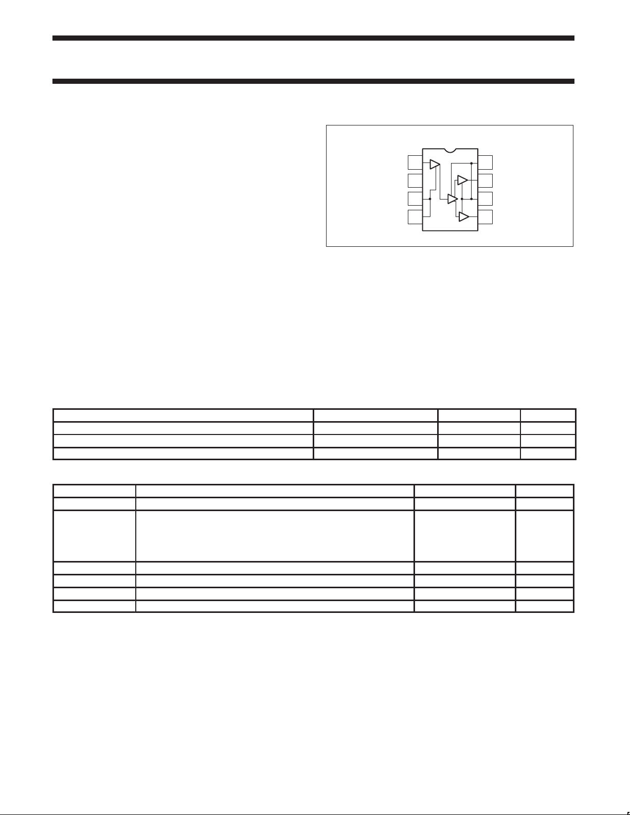
PIN CONFIGURATION
N, FE, D Packages
1
I
IN
2
V
CC
3
GND
1
45
GND
1
Figure 1. Pin Configuration
8
7
6
SD00336
GND
OUT (–)
GND
2
OUT (+)
2
•Differential outputs
•Low input/output impedances
•14kΩ differential transresistance
•ESD hardened
•Wideband gain block
•Medical and scientific instrumentation
•Sensor preamplifiers
•Single-ended to differential conversion
APPLICA TIONS
•Fiber-optic receivers, analog and digital
•Low noise RF amplifiers
•RF signal processing
•Current-to-voltage converters
ORDERING INFORMATION
DESCRIPTION TEMPERATURE RANGE ORDER CODE DWG #
8-Pin Plastic Small Outline (SO) Package -40°C to +85°C SA5212AD SOT96-1
8-Pin Plastic Dual In-Line Package (DIP) -40°C to +85°C SA5212AN SOT97-1
8-Pin Ceramic Dual In-Line Package (DIP) -40°C to +85°C SA5212AFE 0580A
ABSOLUTE MAXIMUM RATINGS
SYMBOL PARAMETER SA5212A UNIT
V
CC
D MAX
I
IN MAX
T
A
T
J
T
STG
NOTES:
1. Maximum dissipation is determined by the operating ambient temperature and the thermal resistance:
2. The use of a pull-up resistor to V
8-Pin Plastic DIP: 110°C/W
8-Pin Plastic SO: 160°C/W
8-Pin Cerdip: 165°C/W
Power Supply 6 V
Power dissipation, TA=25°C (still air)
8-Pin Plastic DIP 1100 mW
8-Pin Plastic SO 750 mW
8-Pin Cerdip 750 mw
Maximum input current
Operating ambient temperature range -40 to 85 °C
Operating junction -55 to 150 °C
Storage temperature range -65 to 150 °C
CC
2
, for the PIN diode, is recommended
1
5 mA
1998 Oct 07 853-1266 20142
2
Philips Semiconductors Product specification
SA5212ATransimpedance amplifier (140MHz)
RECOMMENDED OPERATING CONDITIONS
SYMBOL PARAMETER RATING UNIT
V
CC
T
A
T
J
DC ELECTRICAL CHARACTERISTICS
Minimum and Maximum limits apply over operating temperature range at VCC=5V, unless otherwise specified. Typical data applies at VCC=5V
and T
=25°C1.
A
SYMBOL
V
IN
V
±
O
V
OS
I
CC
I
OMAX
I
IN
I
N MAX
NOTES:
1. As in all high frequency circuits, a supply bypass capacitor should be located as close to the part as possible.
Supply voltage range 4.5 to 5.5 V
Ambient temperature ranges -40 to +85 °C
Junction temperature ranges -40 to +105 °C
PARAMETER TEST CONDITIONS Min Typ Max UNIT
Input bias voltage 0.55 0.8 1.05 V
Output bias voltage 2.5 3.3 3.8 V
Output offset voltage 120 mV
Supply current 20 26 33 mA
Output sink/source current 3 4 mA
Maximum input current (2% linearity) Test Circuit 6, Procedure 2 ±40 ±80 µA
Maximum input current overload threshold T est Circuit 6, Procedure 4 ±60 ±120 µA
1998 Oct 07
3
Philips Semiconductors Product specification
g
T
SA5212ATransimpedance amplifier (140MHz)
AC ELECTRICAL CHARACTERISTICS
Minimum and Maximum limits apply over operating temperature range at VCC=5V, unless otherwise specified. Typical data applies at VCC=5V
and T
=25°C5.
A
SYMBOL
R
R
R
R
f
R
C
T
O
T
O
3dB
IN
IN
Transresistance (differential output)
Output resistance (differential output) DC tested 14 30 46 Ω
Transresistance (single-ended output) DC tested, R
Output resistance (single-ended output) DC tested 7 15 23 Ω
Bandwidth (-3dB) T
Input resistance 70 110 150 Ω
Input capacitance 10 18 pF
∆R/∆V Transresistance power supply sensitivity V
∆R/∆T
I
N
Transresistance ambient
temperature sensitivity
RMS noise current spectral density
(referred to input)
Integrated RMS noise current over the bandwidth (referred to input) C
I
T
C
= 1pF ∆f = 100MHz 32
S
PSRR Power supply rejection ratio
PSRR
V
O MAX
V
IN MAX
t
R
Power supply rejection ratio
(ECL configuration)
Maximum differential output voltage swing
Maximum input amplitude for output duty
cycle of 50 ±5%
Rise time for 50mV output signal
NOTES:
1. Package parasitic capacitance amounts to about 0.2pF.
2. PSRR is output referenced and is circuit board layout dependent at higher frequencies. For best performance use RF filter in V
3. Guaranteed by linearity and over load tests.
defined as 20-80% rise time. It is guaranteed by -3dB bandwidth test.
4. t
R
5. As in all high frequency circuits, a supply bypass capacitor should be located as close to the part as possible.
PARAMETER TEST CONDITIONS Min Typ Max UNIT
DC tested, R
Test Circuit 6, Procedure 1
= ∞
L
= ∞ 4.5 7 9.5 kΩ
L
9.0 14 19 kΩ
Test Circuit 1
D package,
= 25°C 100 140 MHz
A
N, FE packages,
T
= 25°C 100 120
A
= 5 ±0.5V 9.6 %/V
CC
D package
= T
∆T
A
A MAX-TA MIN
Test Circuit 2
f = 10MHz T
T
= 25°C Test Circuit 2
A
= 25°C
A
∆f = 50MHz
1
= 0
S
∆f = 100MHz 27
∆f = 200MHz 40
0.05 %/°C
2.5 pA/√Hz
20
nA
∆f = 50MHz 22
∆f = 200MHz 52
Any package
2
DC tested
∆V
= 0.1V
CC
20 33 dB
Equivalent AC
Test Circuit 3
2
Any package
f = 0.1MHz
1
23 dB
Test Circuit 4
R
= ∞
Test Circuit 6, Procedure 3
L
3
4
Test Circuit 5 325 mV
Test Circuit 5 2.0 ns
1.7 3.2 V
CC
P-P
P-P
line.
1998 Oct 07
4
Philips Semiconductors Product specification
SA5212ATransimpedance amplifier (140MHz)
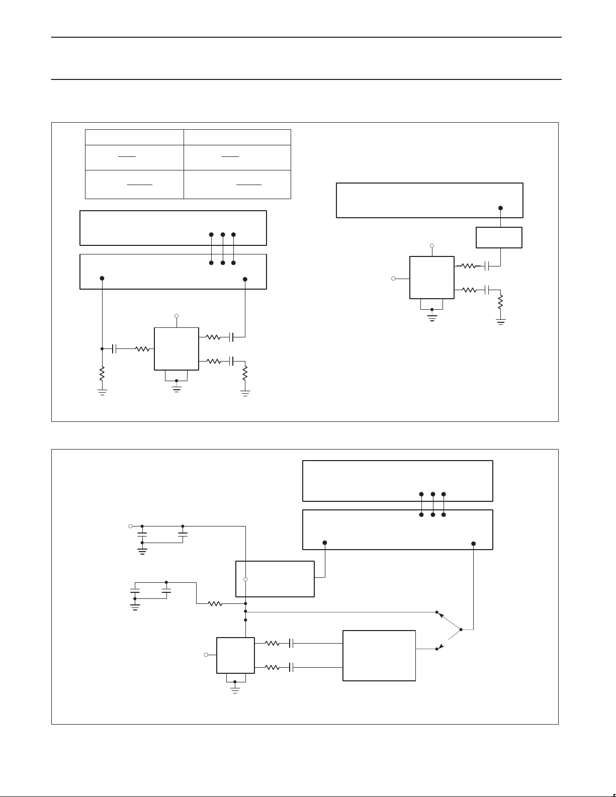
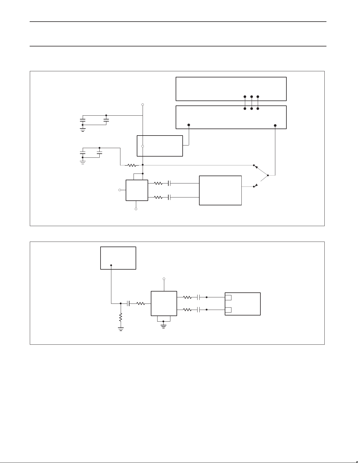
TEST CIRCUITS
SINGLE-ENDED DIFFERENTIAL
Rt
V
OUT
2 S21 RR
V
IN
V
OUT
t
V
IN
4 S21 R
ZO = 50Ω
RO Z
PORT 1
0.1µF
50
1 S22
O
33 RO 2Z
1 S22
NETWORK ANALYZER
S-PARAMETER TEST SET
R = 1k
IN DUT
GND
1
Test Circuit 1
1 S22
1 S22
RL = 50Ω
66
SPECTRUM ANALYZER
V
CC
NC
IN DUT
GND
1
Test Circuit 2
OUT
OUT
GND
AV = 60DB
1µF
33
1µF
33
R
= 50
L
2
SD00337
O
PORT 2
V
CC
1µF
33
OUT
1µF
33
OUT
GND
2
Figure 2. Test Circuits 1 and 2
5V + ∆V
10µF
10µF
0.1µF
10µF
NC
16
GND
V
CC
IN
DUT
1
CURRENT PROBE
1mV/mA
1µF
GND
33
33
1µF
2
OUT
OUT
Test Circuit 3
Figure 3. Test Circuit 3
NETWORK ANALYZER
S-PARAMETER TEST SET
PORT 1 PORT 2
CAL
50
100
BAL.
TRANSFORMER
NH0300HB
UNBAL.
TEST
SD00338
1998 Oct 07
5
Philips Semiconductors Product specification
SA5212ATransimpedance amplifier (140MHz)
TEST CIRCUITS (Continued)
NETWORK ANALYZER
–5.2V + ∆V
10µF
10µF
0.1µF
0.1µF
NC
PULSE GEN.
GND
V
CC
16
1
OUT
IN
OUT
CURRENT PROBE
1mV/mA
GND
2
1µF
33
33
1µF
Test Circuit 4
Figure 4. Test Circuit 4
5V
S-PARAMETER TEST SET
PORT 1 PORT 2
CAL
50
100
BAL.
TRANSFORMER
NH0300HB
UNBAL.
TEST
SD00339
1998 Oct 07
50
0.1µF
GND
1
OUT
DUT
OUT
GND
IN
1k
Test Circuit 5
Figure 5. Test Circuit 5
1µF
33
33
1µF
2
A
Z
= 50Ω
O
OSCILLOSCOPE
B
ZO = 50Ω
Measurement done using
differential wave forms
SD00545
6
 Loading...