

Philips SA5211D Datasheet

INTEGRATED CIRCUITS
SA5211
Transimpedance amplifier (180MHz)
Product specification
Replaces datasheet NE/SA5211 of 1995 Apr 26
IC19 Data Handbook
1998 Oct 07
Philips Semiconductors Product specification
SYMBOL
PARAMETER
RATING
UNIT
SA521 1Transimpedance amplifier (180MHz)
DESCRIPTION
The SA521 1 is a 28kΩ transimpedance, wide-band, low noise
amplifier with differential outputs, particularly suitable for signal
recovery in fiber optic receivers. The part is ideally suited for many
other RF applications as a general purpose gain block.
FEA TURES
•Extremely low noise:
1.8pA Hz
•Single 5V supply
•Large bandwidth: 180MHz
•Differential outputs
•Low input/output impedances
•High power supply rejection ratio
•28kΩ differential transresistance
APPLICATIONS
•Fiber optic receivers, analog and digital
•Current-to-voltage converters
•Wide-band gain block
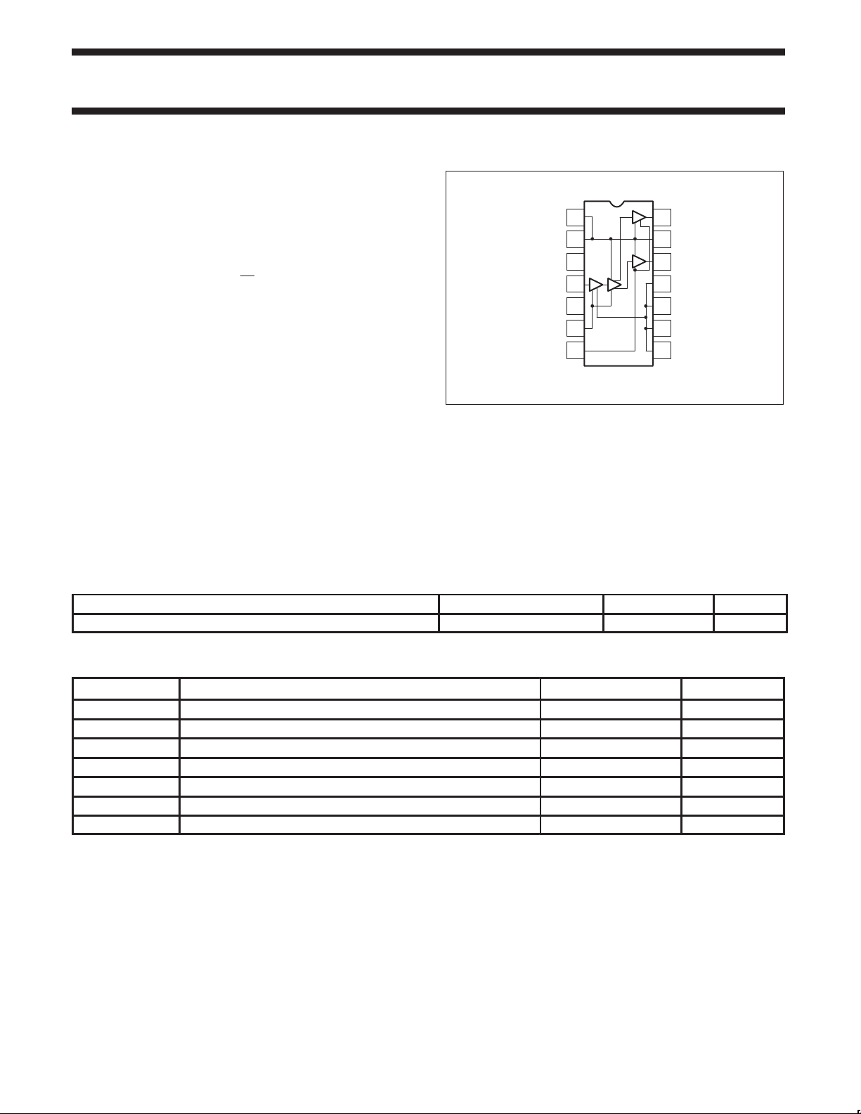
PIN CONFIGURATION
D Package
1
GND
2
2
GND
2
3
NC
4
I
IN
5
NC
6
V
CC1
78
V
CC2
TOP VIEW
Figure 1. Pin Configuration
•Medical and scientific Instrumentation
•Sensor preamplifiers
•Single-ended to differential conversion
•Low noise RF amplifiers
•RF signal processing
14
OUT (–)
13
GND
12
OUT (+)
11
GND
10
GND
9
GND
GND
SD00318
2
1
1
1
1
ORDERING INFORMATION
DESCRIPTION TEMPERATURE RANGE ORDER CODE DWG #
14-Pin Plastic Small Outline (SO) Package -40 to +85°C SA5211D SOT108-1
ABSOLUTE MAXIMUM RATINGS
V
CC
T
A
T
J
T
STG
P
D MAX
I
IN MAX
θ
JA
NOTES:
1. Maximum dissipation is determined by the operating ambient temperature and the thermal resistance:
=125°C/W
θ
2. The use of a pull-up resistor to V
JA
Power supply 6 V
Operating ambient temperature range -40 to +85 °C
Operating junction temperature range -55 to +150 °C
Storage temperature range -65 to +150 °C
Power dissipation, TA=25°C (still-air)
Maximum input current
2
1
1.0 W
5 mA
Thermal resistance 125 °C/W
, for the PIN diode is recommended.
CC
1998 Oct 07 853-1799 20142
2
Philips Semiconductors Product specification
SA521 1Transimpedance amplifier (180MHz)
RECOMMENDED OPERATING CONDITIONS
SYMBOL PARAMETER RATING UNIT
V
CC
T
A
T
J
DC ELECTRICAL CHARACTERISTICS
Min and Max limits apply over operating temperature range at VCC=5V, unless otherwise specified. Typical data apply at VCC=5V and TA=25°C.
SYMBOL
V
IN
V
±
O
V
OS
I
CC
I
OMAX
I
IN
I
IN MAX
NOTES:
1. Test condition: output quiescent voltage variation is less than 100mV for 3mA load current.
Input bias voltage 0.55 0.8 1.00 V
Output bias voltage 2.7 3.4 3.7 V
Output offset voltage 0 130 mV
Supply current 20 26 31 mA
Output sink/source current
Input current
(2% linearity)
Maximum input current
overload threshold
Supply voltage 4.5 to 5.5 V
Ambient temperature range -40 to +85 °C
Junction temperature range -40 to +105 °C
PARAMETER TEST CONDITIONS Min Typ Max UNIT
1
Test Circuit 8,
Procedure 2
Test Circuit 8,
Procedure 4
3 4 mA
±20 ±40 µA
±30 ±60 µA
1998 Oct 07
3
Philips Semiconductors Product specification
1
SA521 1Transimpedance amplifier (180MHz)
AC ELECTRICAL CHARACTERISTICS
Typical data and Min and Max limits apply at VCC=5V and TA=25°C
SYMBOL
R
R
R
R
f
R
C
T
O
T
O
3dB
IN
IN
Transresistance (differential output)
Output resistance (differential output) DC tested 30 Ω
Transresistance (single-ended output)
Output resistance (single-ended output) DC tested 15 Ω
Bandwidth (-3dB)
Input resistance 200 Ω
Input capacitance 4 pF
∆R/∆V Transresistance power supply sensitivity V
∆R/∆T Transresistance ambient temperature sensitivity ∆T
I
N
I
T
RMS noise current spectral density (referred to
input)
Integrated RMS noise current over the bandwidth
(referred to input)
CS=0
CS=1pF ∆f = 100MHz 21 nA
PSRR
Power supply rejection ratio
(V
= V
CC1
PSRR Power supply rejection ratio2 (V
PSRR Power supply rejection ratio2 (V
PSRR Power supply rejection ratio (ECL configuration)
V
OMAX
V
IN MAX
t
R
Maximum differential output voltage swing
Maximum input amplitude for output duty cycle of
3
50±5%
Rise time for 50mV output signal
NOTES:
1. Package parasitic capacitance amounts to about 0.2pF
2. PSRR is output referenced and is circuit board layout dependent at higher frequencies. For best performance use RF filter in V
3.
Guaranteed by linearity and overload tests.
4. t
defined as 20-80% rise time. It is guaranteed by -3dB bandwidth test.
R
PARAMETER TEST CONDITIONS Min Typ Max UNIT
DC tested R
Test Circuit 8, Procedure 1
DC tested
T
A
Test circuit 1
CC
= T
A
= ∞
L
= ∞
R
L
= 25°C
= 5±0.5V 3.7 %/V
A MAX-TA MIN
21 28 36 kΩ
10.5 14 18.0 kΩ
180 MHz
0.025 %/°C
Test Circuit 2
f = 10MHz
T
= 25°C
A
T
= 25°C
A
1.8 pA/√Hz
Test Circuit 2
∆f = 50MHz 13
∆f = 100MHz 20 nA
∆f = 200MHz 35
∆f = 50MHz 13
∆f = 200MHz 41
CC
CC
= 0.1V
= 0.1V
23 32 dB
23 32 dB
CC2
2
)
DC tested, ∆V
Equivalent AC
Test Circuit 3
DC tested, ∆V
CC1
)
Equivalent AC
Test Circuit 4
CC2
DC tested, ∆V
)
Equivalent AC
CC
= 0.1V
45 65 dB
Test Circuit 5
2
f = 0.1MHz
Test Circuit 6
R
= ∞
L
Test Circuit 8, Procedure 3
23 dB
1.7 3.2 V
Test Circuit 7 160 mV
4
Test Circuit 7 0.8 1.8 ns
CC
P-P
P-P
lines.
1998 Oct 07
4
Philips Semiconductors Product specification
SA521 1Transimpedance amplifier (180MHz)
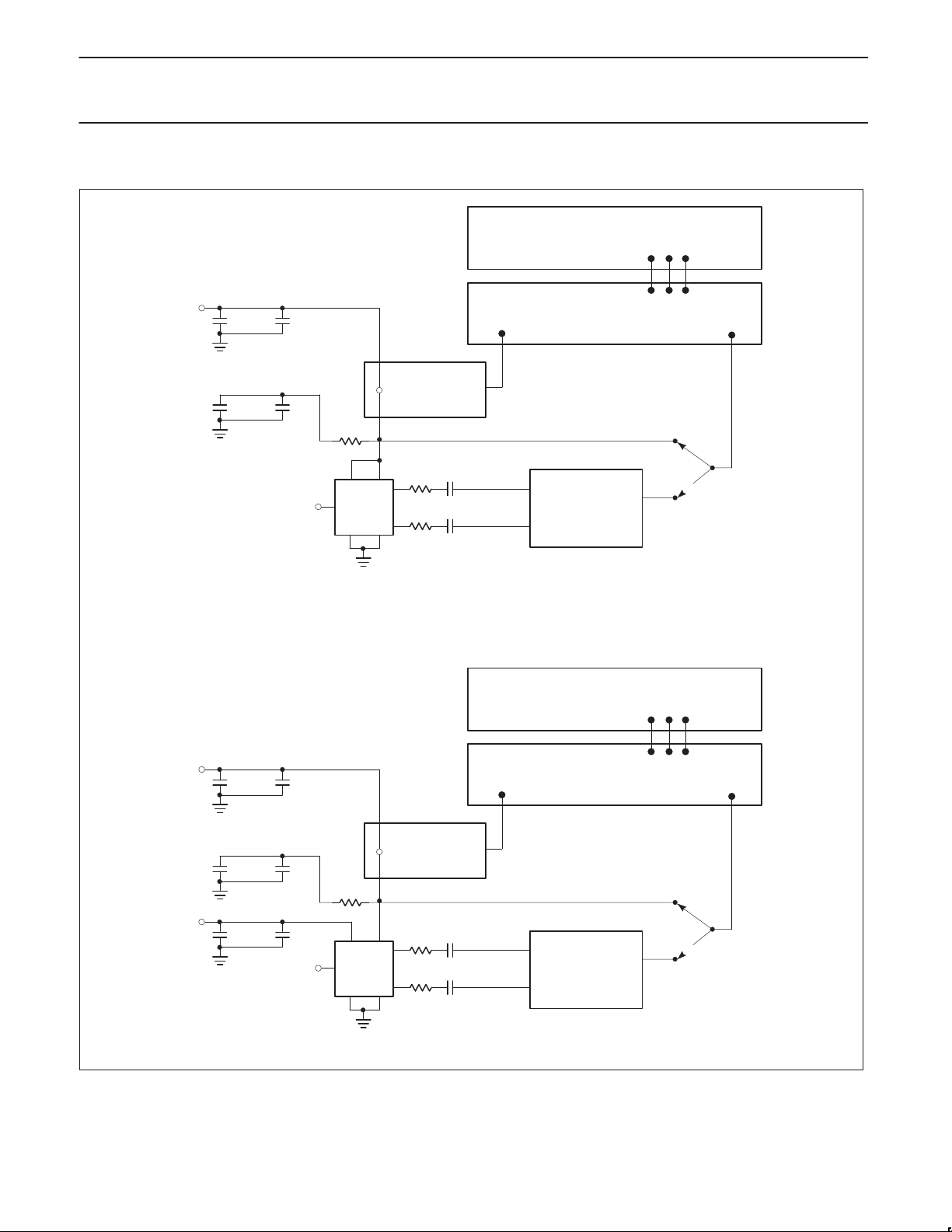
TEST CIRCUITS
ZO = 50
NETWORK ANALYZER
S-PARAMETER TEST SET
PORT 1
0.1µF
R = 1k
50
5V
V
CC1VCC2
IN DUT
GND
1
OUT
OUT
GND
PORT 2
0.1µF
33
0.1µF
33
2
Test Circuit 1
SPECTRUM ANALYZER
V
CC1VCC2
NC
IN DUT
GND
SINGLE-ENDED DIFFERENTIAL
V
OUT
RT[
RO[ Z
= 50
Z
O
= 50
R
L
5V
33
OUT
33
OUT
GND
1
2
R + 2 @ S21 @ RRT+
V
IN
1 ) S22
Ť
Ť
O
AV = 60DB
0.1µF
0.1µF
* 33 RO+ 2Z
1 * S22
= 50
Z
O
R
= 50
L
V
OUT
V
IN
1 ) S22
Ť
O
1 * S22
R + 4 @ S21 @ R
Ť
* 66
1998 Oct 07
Test Circuit 2
Figure 2. Test Circuits 1 and 2
5
SD00319
Philips Semiconductors Product specification
SA521 1Transimpedance amplifier (180MHz)
TEST CIRCUITS (Continued)
NETWORK ANALYZER
5V
10µF
10µF
0.1µF
0.1µF
IN
V
GND
CC1
16
1
CURRENT PROBE
1mV/mA
V
CC2
GND
33
33
2
OUT
OUT
0.1µF
0.1µF
PORT 1 PORT 2
100
BAL.
S-PARAMETER TEST SET
TRANSFORMER
NH0300HB
50
UNBAL.
CAL
TEST
Test Circuit 3
NETWORK ANALYZER
1998 Oct 07
5V
5V
10µF
10µF
10µF
0.1µF
0.1µF
0.1µF
IN
V
CC2
GND
PORT 1 PORT 2
CURRENT PROBE
1mV/mA
16
V
CC1
OUT
OUT
1
GND
0.1µF
33
100
33
0.1µF
2
BAL.
Test Circuit 4
S-PARAMETER TEST SET
TRANSFORMER
NH0300HB
50
UNBAL.
CAL
TEST
SD00320
Figure 3. Test Circuits 3 and 4
6
 Loading...