

Page 1

1. Description
2. Features
SA5211
Transimpedance amplifier (180 MHz)
Rev. 03 — 07 October 1998 Product specification
The SA5211 is a 28 kΩ transimpedance, wide-band, low noise amplifier with
differential outputs, particularly suitable for signal recovery in fiber optic receivers.
The part is ideally suited for many other RF applications as a general purpose gain
block.
■ Extremely low noise: 1.8 pA / √Hz
■ Single 5 V supply
■ Large bandwidth: 180 MHz
■ Differential outputs
■ Low input/output impedances
■ High power supply rejection ratio
■ 28 kΩ differential transresistance
3. Applications
c
c
■ Fiber optic receivers, analog and digital
■ Current-to-voltage converters
■ Wide-band gain block
■ Medical and scientific Instrumentation
■ Sensor preamplifiers
■ Single-ended to differential conversion
■ Low noise RF amplifiers
■ RF signal processing
Page 2
Philips Semiconductors
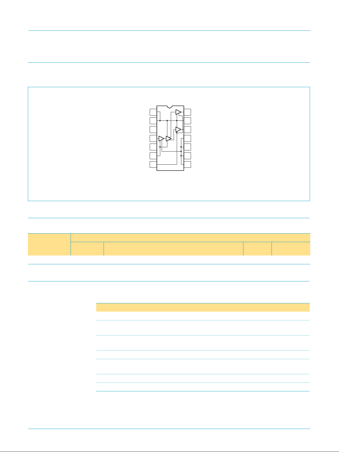
4. Pinning information
4.1 Pinning
SA5211
Transimpedance amplifier (180 MHz)
D Package
1
GND
2
2
GND
2
3
NC
4
I
IN
5
NC
6
V
CC1
78
V
CC2
TOP VIEW
14
OUT (–)
13
GND
12
OUT (+)
11
GND
10
GND
9
GND
GND
SD00318
2
1
1
1
1
Fig 1. Pin configuration.
5. Ordering information
Table 1: Ordering information
Type number Package
Name Description Version Temperature
range (°C)
SA5211D SO14 plastic small outline package; 14 leads; body width 3.9 mm SOT108-1 −40 to +85
6. Limiting values
Table 2: Limiting values
In accordance with the Absolute Maximum Rating System (IEC 60134).
Symbol Parameter Conditions Min Max Unit
V
CC
T
amb
power supply − 6V
operating ambient
-40 +85 °C
temperature range
T
J
operating junction
-55 +150 °C
temperature range
T
STG
P
D MAX
I
IN MAX
θ
JA
[1] Maximum dissipation is determined by the operating ambient temperature and the thermal resistance:
[2] The use of a pull-up resistor to V
9397 750 07427
Product specification Rev. 03 — 07 October 1998 2 of 28
storage temperature range -65 +150 °C
power dissipation, TA=25°C
(still-air)
maximum input current
[1]
[2]
− 1.0 W
− 5mA
thermal resistance − 125 °C/W
θJA= 125 °C/W
, for the PIN diode is recommended.
CC
© Philips Electronics N.V. 2001. All rights reserved.
Page 3

Philips Semiconductors
SA5211
Transimpedance amplifier (180 MHz)
Table 3: Recommended operating conditions
Symbol Parameter Conditions Min Max Unit
V
CC
T
amb
T
J
supply voltage 4.5 5.5 V
ambient temperature range -40 +85 °C
junction temperature range -40 +105 °C
7. Static characteristics
Table 4: DC electrical characteristics
Min and Max limits apply over operating temperature range at VCC= 5 V, unless otherwise specified. Typical data apply at
= 5 V and T
V
CC
Symbol Parameter Test conditions Min Typ Max Unit
V
IN
V
O±
V
OS
I
CC
I
OMAX
I
IN
I
IN MAX
=25°C.
amb
input bias voltage 0.55 0.8 1.00 V
output bias voltage 2.7 3.4 3.7 V
output offset voltage − 0 130 mV
supply current 20 26 31 mA
output sink/source current
input current
(2% linearity)
maximum input current
overload threshold
[1]
Test Circuit 8,
Procedure 2
Test Circuit 8,
Procedure 4
34− mA
±20 ±40 −µA
±30 ±60 −µA
[1] Test condition: output quiescent voltage variation is less than 100 mV for 3 mA load current.
8. Dynamic characteristics
Table 5: AC electrical characteristics
Typical data and Min and Max limits apply at VCC= 5 V and T
Symbol Parameter Test conditions Min Typ Max Unit
R
R
R
R
f
R
C
T
O
T
O
3dB
IN
IN
transresistance (differential output) DC tested RL = ∞
output resistance (differential output) DC tested − 30 −Ω
transresistance (single-ended output) DC tested
output resistance (single-ended output) DC tested − 15 −Ω
bandwidth (-3dB) TA = 25°C
input resistance − 200 −Ω
input capacitance − 4 − pF
∆R/∆V transresistance power supply sensitivity V
∆R/∆T transresistance ambient temperature sensitivity ∆T
I
N
RMS noise current spectral density (referred to
input)
I
T
integrated RMS noise current over the
bandwidth (referred to input)
=25°C
amb
21 28 36 kΩ
Test Circuit 8, Procedure 1
10.5 14 18.0 kΩ
RL = ∞
− 180 − MHz
Test circuit 1
= 5±0.5 V − 3.7 − %/V
CC
= T
amb
amb MAX-Tamb MIN
Test Circuit 2
− 0.025 − %/°C
− 1.8 − pA/√Hz
f = 10 MHz
TA = 25 °C
TA = 25 °C
−−−−
Test Circuit 2
9397 750 07427
Product specification Rev. 03 — 07 October 1998 3 of 28
© Philips Electronics N.V. 2001. All rights reserved.
Page 4

Philips Semiconductors
SA5211
Transimpedance amplifier (180 MHz)
Table 5: AC electrical characteristics
Typical data and Min and Max limits apply at VCC= 5 V and T
…continued
amb
=25°C
Symbol Parameter Test conditions Min Typ Max Unit
I
n
I
n
PSRR power supply rejection ratio
[1]
CS=0
∆f = 50 MHz
∆f = 100 MHz
∆f = 200 MHz
CS= 1pF ∆f = 50 MHz
∆f = 100 MHz
∆f = 200 MHz
(V
CC1
= V
CC2
[2]
)
DC tested, ∆V
Equivalent AC
= 0.1V
CC
−
13
−
nA
−
20
−
−
35
−
−
13
−
nA
−
21
−
−
41
−
23 32 − dB
Test Circuit 3
PSRR power supply rejection ratio
) DC tested, ∆VCC = 0.1V
CC1
23 32 − dB
[2]
(V
Equivalent AC
Test Circuit 4
PSRR power supply rejection ratio
[2]
(V
) DC tested, ∆VCC = 0.1V
CC2
45 65 − dB
Equivalent AC
Test Circuit 5
PSRR power supply rejection ratio (ECL
[2]
V
OMAX
configuration)
maximum differential output voltage swing RL = ∞
f = 0.1 MHz
Test Circuit 6
− 23 − dB
1.7 3.2 − V
Test Circuit 8, Procedure 3
V
IN MAX
t
R
maximum input amplitude for output duty cycle
of 50±5%
rise time for 50mV output signal
[3]
[4]
Test Circuit 7 160 −−mV
Test Circuit 7 − 0.8 1.8 ns
P-P
P-P
[1] Package parasitic capacitance amounts to about 0.2pF
[2] PSRR is output referenced and is circuit board layout dependent at higher frequencies. For best performance use RF filter in VCC lines.
[3] Guaranteed by linearity and overload tests.
[4] tR defined as 20 to 80% rise time. It is guaranteed by -3dB bandwidth test.
9397 750 07427
Product specification Rev. 03 — 07 October 1998 4 of 28
© Philips Electronics N.V. 2001. All rights reserved.
Page 5
Philips Semiconductors
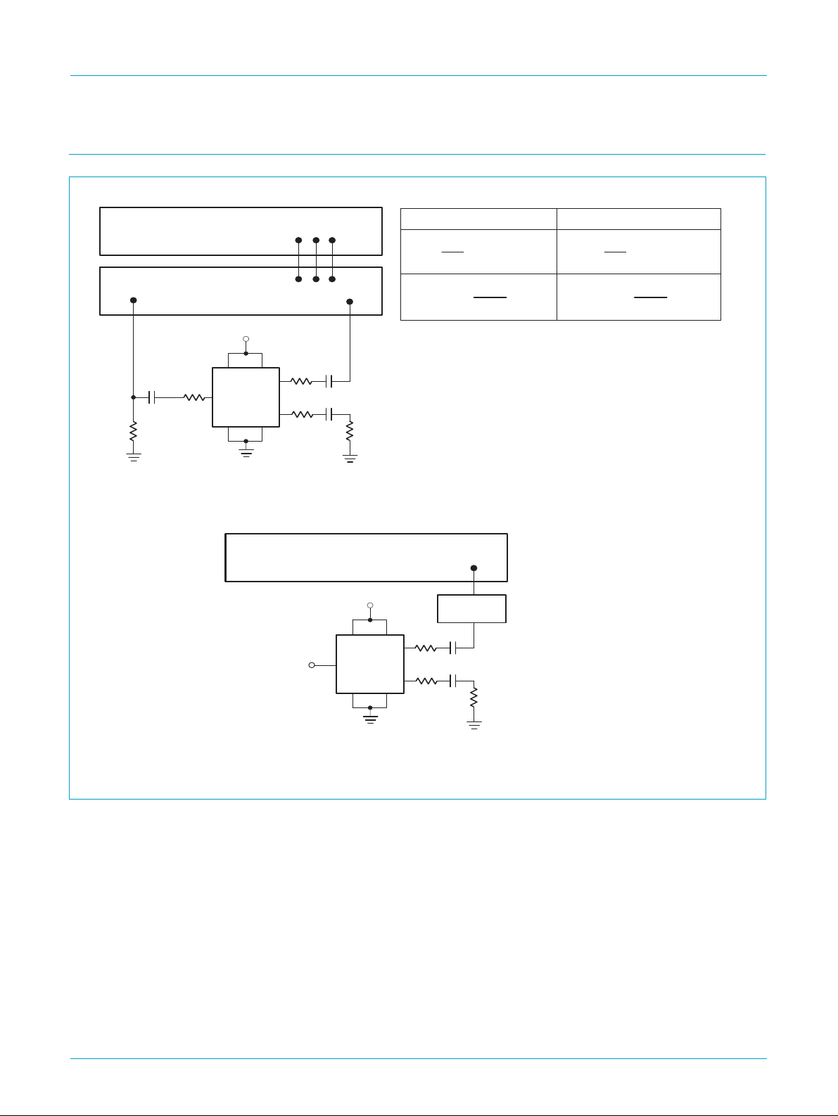
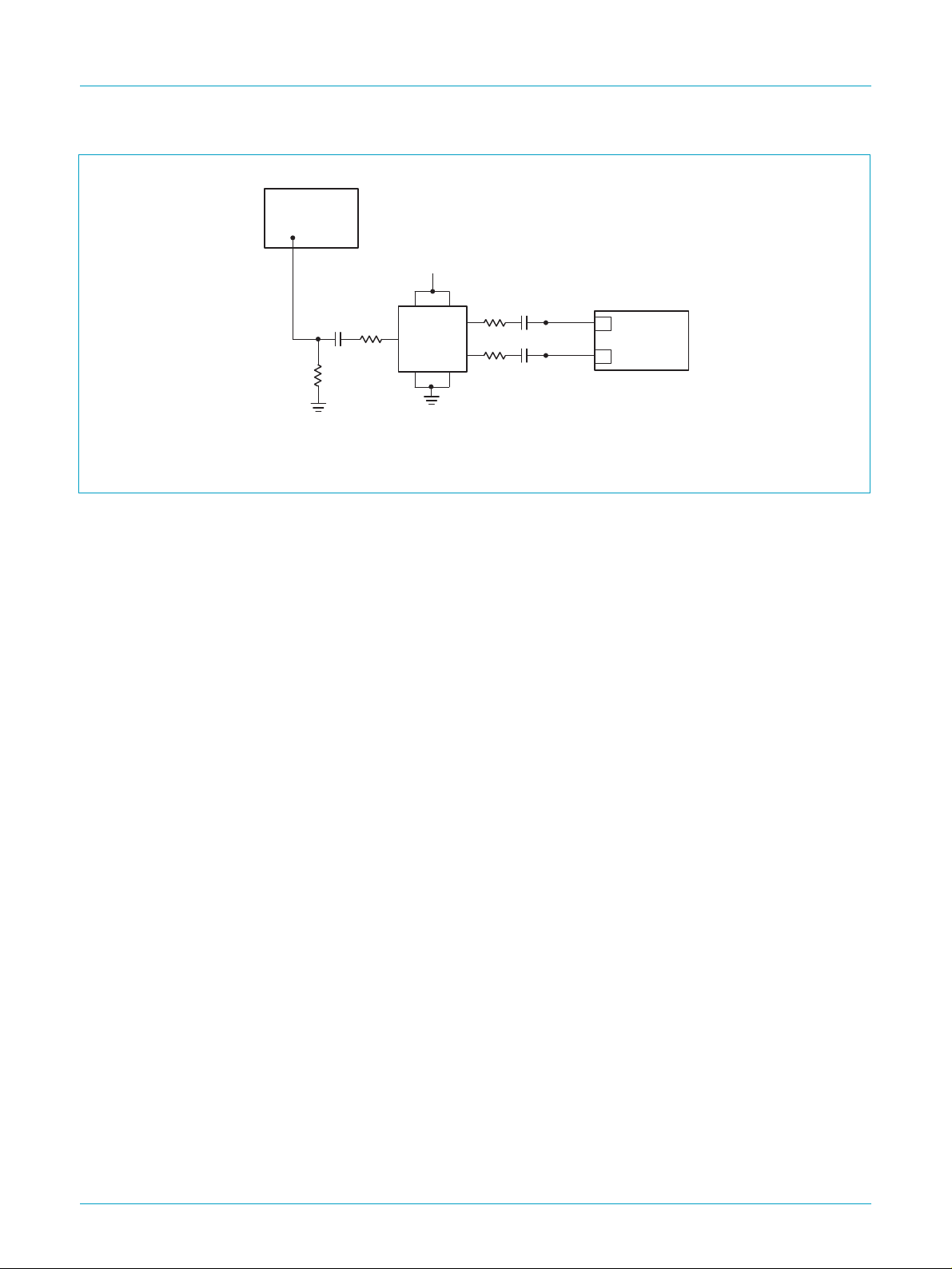
9. Test circuits
SA5211
Transimpedance amplifier (180 MHz)
ZO = 50
PORT 1
0.1µF
50
NETWORK ANALYZER
S-PARAMETER TEST SET
5V
V
R = 1k
GND
CC1
IN DUT
1
V
CC2
OUT
OUT
GND
PORT 2
0.1µF
33
0.1µF
33
2
Test Circuit 1
SPECTRUM ANALYZER
V
CC1
NC
IN DUT
GND
SINGLE-ENDED DIFFERENTIAL
V
OUT
RT
RO ≈ Z
Z
= 50
O
= 50
R
L
5V
V
CC2
33
OUT
GND
33
2
OUT
1
R = 2 × S21 × RR
≈
V
IN
1 + S22
O
1 – S22
AV = 60DB
0.1µF
0.1µF
– 33 RO = 2Z
= 50
Z
O
= 50
R
L
V
OUT
=
T
V
IN
R = 4 × S21 × R
1 + S22
O
1 – S22
– 66
Test Circuit 2
SD00319
Fig 2. Test circuits 1 and 2.
9397 750 07427
Product specification Rev. 03 — 07 October 1998 5 of 28
© Philips Electronics N.V. 2001. All rights reserved.
Page 6
Philips Semiconductors
SA5211
Transimpedance amplifier (180 MHz)
NETWORK ANALYZER
5V
10µF
10µF
0.1µF
0.1µF
IN
V
GND
CC1
16
1
CURRENT PROBE
1mV/mA
V
CC2
GND
33
33
2
OUT
OUT
0.1µF
0.1µF
PORT 1 PORT 2
100
BAL.
S-PARAMETER TEST SET
TRANSFORMER
NH0300HB
50
UNBAL.
CAL
TEST
Test Circuit 3
NETWORK ANALYZER
5V
10µF
0.1µF
PORT 1 PORT 2
S-PARAMETER TEST SET
CURRENT PROBE
OUT
OUT
V
GND
CC1
1mV/mA
33
33
2
Test Circuit 4
0.1µF
0.1µF
100
BAL.
TRANSFORMER
NH0300HB
50
UNBAL.
CAL
TEST
SD00320
10µF
0.1µF
5V
10µF
0.1µF
16
V
CC2
IN
GND
1
Fig 3. Test circuits 3 and 4.
9397 750 07427
Product specification Rev. 03 — 07 October 1998 6 of 28
© Philips Electronics N.V. 2001. All rights reserved.
Page 7
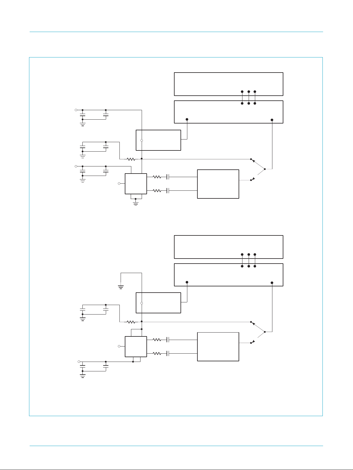
Philips Semiconductors
SA5211
Transimpedance amplifier (180 MHz)
NETWORK ANALYZER
5V
5V
10µF
10µF
10µF
0.1µF
0.1µF
0.1µF
IN
V
GND
CC1
PORT 1 PORT 2
CURRENT PROBE
1mV/mA
16
V
CC2
OUT
OUT
1
GND
0.1µF
33
100
33
0.1µF
2
BAL.
S-PARAMETER TEST SET
TRANSFORMER
NH0300HB
50
UNBAL.
CAL
TEST
Test Circuit 5
NETWORK ANALYZER
S-PARAMETER TEST SET
GND
PORT 1 PORT 2
CURRENT PROBE
OUT
OUT
V
GND
CC2
1mV/mA
2
0.1µF
33
33
Test Circuit 6
0.1µF
100
BAL.
TRANSFORMER
NH0300HB
50
UNBAL.
CAL
TEST
SD00321
5.2V
10µF
10µF
0.1µF
0.1µF
16
GND
1
IN
V
CC1
Fig 4. Test circuits 5 and 6.
9397 750 07427
Product specification Rev. 03 — 07 October 1998 7 of 28
© Philips Electronics N.V. 2001. All rights reserved.
Page 8
Philips Semiconductors
PULSE GEN.
50
0.1µF
1k
V
CC1VCC2
IN
DUT
GND
1
OUT
OUT
GND
SA5211
Transimpedance amplifier (180 MHz)
0.1µF
33
33
0.1µF
2
A
Z
= 50Ω
O
OSCILLOSCOPE
B
Z
= 50Ω
O
Measurement done using
differential wave forms
Fig 5. Test circuit 7.
Test Circuit 7
SD00322
9397 750 07427
© Philips Electronics N.V. 2001. All rights reserved.
Product specification Rev. 03 — 07 October 1998 8 of 28
Page 9
Philips Semiconductors
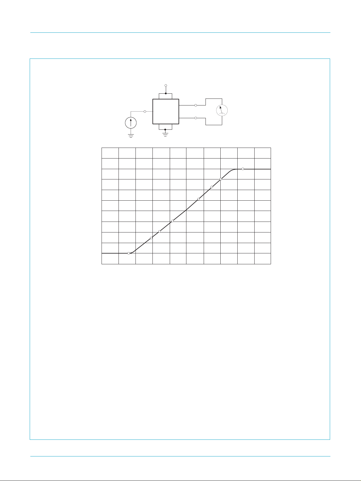
Typical Differential Output Voltage
vs Current Input
5V
SA5211
Transimpedance amplifier (180 MHz)
OUT +
IN
DUT
GND
1
OUT –
GND
2
CURRENT INPUT (µA)
IIN (µA)
2.00
1.60
1.20
0.80
0.40
0.00
–0.40
–0.80
DIFFERENTIAL OUTPUT VOLTAGE (V)
–1.20
–1.60
–2.00
–100 –80 –60 –40 –20 0 20 40 60 80 100
+
V
(V)
OUT
–
NE5211 TEST CONDITIONS
Procedure 1 R
Procedure 2 Linearity = 1 – ABS((V
Procedure 3 V
Procedure 4 I
Test Circuit 8
measured at 15µA
T
R
= (VO1 – VO2)/(+15µA – (–15µA))
T
Where: V
Where: V
Where: VO7 Measured at IIN = +65µA
IN
V
Where: V
Measured at IIN = +15µA
O1
Measured at IIN = –15µA
V
O2
– VOB) / (VO3 – VO4))
OA
Measured at IIN = +30µA
O3
Measured at IIN = –30µA
V
O4
VOA = RT × (+ 30 µA) + V
VOB = RT × (– 30 µA) + V
= VO7 – V
OMAX
Test Pass Conditions:
– VO5 > 20mV and V06 – VO5 > 50mV
O7
O8
Measured at IIN = –65µA
V
O8
Measured at IIN = +40µA
O5
Measured at IIN = –400µA
V
O6
V
Measured at IIN = +65µA
O7
Measured at IIN = –65µA
V
O8
OB
OB
SD00331
Fig 6. Test circuit 8.
9397 750 07427
Product specification Rev. 03 — 07 October 1998 9 of 28
© Philips Electronics N.V. 2001. All rights reserved.
Page 10

Philips Semiconductors
10. Typical performance characteristics
SA5211
Transimpedance amplifier (180 MHz)
NE5211 Supply Current
vs Temperature
30
28
26
CC2
24
CC1
(I + I )
22
TOTALSUPPLY CURRENT (mA)
20
18
60 20 0 20 40 60 80 100 120
5.5V
5.0V
4.5V
40
AMBIENT TEMPERATURE (°C)
NE5211 Input Bias Voltage
vs Temperature
950
900
850
800
750
700
INPUT BIAS VOLTAGE (mV)
650
5.5V
4.5V
60 20 0 20 40 60 80 100 12040 140
AMBIENT TEMPERATURE (°C)
140
NE5211 Output Bias Voltage
vs Temperature
3.50
VCC= 5.0V
3.45
PIN 14
3.40
3.35
PIN 12
3.30
OUTPUT BIAS VOLTAGE (V)
3.25
60 20 0 20 40 60 80 100 12040 140
AMBIENT TEMPERATURE (°C)
NE5211 Output Bias Voltage
4.1
3.9
3.7
3.5
3.3
3.1
2.9
OUTPUT BIAS VOLTAGE (V)
2.7
60 20 0 20 40 60 80 100 12040 140
vs Temperature
PIN 14
5.5V
5.0V
4.5V
AMBIENT TEMPERATURE (°C)
NE5211 Output Voltage
vs Input Current
2.0
0
55°C
DIFFERENTIAL OUTPUT VOLTAGE (V)
+125°C
2.0
100.0 0 +100.0
+85°C
INPUT CURRENT (mA)
+85°C
+25°C
+125°C
55°C
NE5211 Differential Output Voltage
vs Input Current
2.0
0
4.5V
5.5V
DIFFERENTIAL OUTPUT VOLTAGE (V)
2.0
100.0 0 +100.0
5.0V
INPUT CURRENT (mA)
5.5V5.0V
4.5V
+25°C
NE5211 Output Offset Voltage
vs Temperature
40
VOS=V
20
0
20
40
60
80
100
120
OUTPUT OFFSET VOLTAGE (mV)
140
60 20 0 20 40 60 80 100 12040 140
OUT12VOUT14
4.5V
5.0V
5.5V
AMBIENT TEMPERATURE (°C)
NE5211 Differential Output Swing
vs Temperature
4.0
3.8
DC TESTED
=
¥
R
L
3.6
5.5V
3.4
3.2
5.0V
3.0
2.8
4.5V
2.6
2.4
DIFFERENTIAL OUTPUT SWING (V)
2.2
60 20 0 20 40 60 80 100 12040 140
AMBIENT TEMPERATURE (°C)
NE5211 Output Voltage
vs Input Current
+125°C
4.5
OUTPUT VOLTAGE (V)
2.5
100.0 0 +100.0
INPUT CURRENT (mA)
+85°C
+25°C
+125°C
+25°C
55°C
+85°C
55°C55°C
+85°C
+25°C
SD00332
+125°C
Fig 7. Typical performance characteristics.
9397 750 07427
Product specification Rev. 03 — 07 October 1998 10 of 28
© Philips Electronics N.V. 2001. All rights reserved.
Page 11

Philips Semiconductors
()
SA5211
Transimpedance amplifier (180 MHz)
NE5211 Gain vs Frequency NE5211 Gain vs Frequency
17
16
15
14
13
PIN 12
12
=25°C
T
A
GAIN (dB)
=50
W
R
11
L
10
9
8
0.1 1 10 100
FREQUENCY (MHz)
5.5V
5.0V
4.5V
NE5211 Gain vs Frequency
17
16
15
14
13
PIN 12
12
V
=5V
CC
GAIN (dB)
11
10
9
8
0.1 1 10 100
FREQUENCY (MHz)
55°C
125°C
85°C
25°C
17
16
15
14
13
PIN 14
12
T
=25°C
A
GAIN (dB)
11
R
=50
W
L
10
9
8
0.1 1 10 100
FREQUENCY (MHz)
NE5211 Gain vs Frequency
17
16
15
14
13
PIN 14
12
V
=5V
CC
GAIN (dB)
11
10
9
8
0.1 1 10 100
FREQUENCY (MHz)
5.5V
5.0V
55°C
4.5V
125°C
85°C
25°C
NE5211 Differential Transresistance
vs Temperature
33
W
DC TESTED
32
R
=
¥
L
31
30
5.5V
29
5.0V
28
4.5V
DIFFERENTIAL TRANSRESISTANCE (k )
27
60 40 20 0 20 40 10060 12080
AMBIENT TEMPERATURE (°C)
NE5211 Typical
Bandwidth Distribution
(70 Parts from 3 Wafer Lots)
60
PIN 12
SINGLE-ENDED
50
=50
W
R
L
40
30
20
POPULATION (%)
10
0
143 155 167 179 191 203
FREQUENCY (MHz)
V
T
CC
A
=25°C
140
= 5.0V
NE5211 Bandwidth
vs Temperature
220
5.5V
200
5.0V
180
4.5V
160
140
BANDWIDTH (MHz)
120
100
60 40 20 0 20 40 10060 12080
AMBIENT TEMPERATURE (°C)
PIN 12
SINGLE-ENDED
R
=50
W
L
140
NE5211 Gain and Phase
Shift vs Frequency
17
16
15
14
13
12
GAIN (dB)
PIN 12
11
10
9
8
=5V
V
CC
=25°C
T
A
0.1 1 10 100
FREQUENCY (MHz)
120
60
0
60
120
o
PHASE ( )
NE5211 Gain and Phase
Shift vs Frequency
17
16
15
14
13
12
GAIN (dB)
PIN 14
11
V
=5V
CC
10
T
=25°C
A
9
8
0.1 1 10 100
FREQUENCY (MHz)
120
270
SD00333
o
Fig 8. Typical performance characteristics. (cont.)
9397 750 07427
Product specification Rev. 03 — 07 October 1998 11 of 28
© Philips Electronics N.V. 2001. All rights reserved.
PHASE
Page 12

Philips Semiconductors
SA5211
Transimpedance amplifier (180 MHz)
NE5211 Output Resistance
vs Temperature
18
= 5.0V
V
CC
DC TESTED
17
W
16
15
14
OUTPUT RESISTANCE ( )
13
60 40 20 0 20 40 10060 12080
PIN 14
PIN 12
AMBIENT TEMPERATURE (°C)
NE5211 Output Resistance
vs Frequency
40
W
35
PIN 12
30
T
=25°C
A
25
20
15
10
5
OUTPUT RESISTANCE ( )
0
0.1 1 10 100
4.5V 5.0V
5.5V
FREQUENCY (MHz)
140
NE5211 Output Resistance
vs Temperature
18
PIN 12
DC TESTED
17
W
16
15
14
OUTPUT RESISTANCE ( )
13
60 40 20 0 20 40 10060 12080
4.5V
5.0V
5.5V
AMBIENT TEMPERATURE (°C)
NE5211 Output Resistance
80
W
70
60
50
40
30
20
10
OUTPUT RESISTANCE ( )
0
0.1 1 10 100
vs Frequency
VCC= 5.0V
FREQUENCY (MHz)
+125°C
+85°C
+25°C
55°C
140
NE5211 Output Resistance
vs Temperature
19
PIN 14
DC TESTED
18
W
17
16
15
OUTPUT RESISTANCE ( )
14
60 40 20 0 20 40 10060 12080
4.5V
5.0V
5.5V
AMBIENT TEMPERATURE (°C)
NE5211 Output Resistance
80
W
70
60
50
40
30
20
10
OUTPUT RESISTANCE ( )
0
0.1 1 10 100
vs Frequency
VCC= 5.0V
PIN 14
FREQUENCY (MHz)
140
PIN 12
NE5211 Power Supply Rejection Ratio
vs Temperature
40
V
CC1=VCC2
38
D
V
CC
DC TESTED
OUTPUT REFERRED
36
34
32
30
POWER SUPPLY REJECTION RATIO (dB)
28
60 40 20 0 20 40 10060 12080
AMBIENT TEMPERATURE (°C)
= 5.0V
=±0.1V
140
10
DELAY (ns)
NE5211 Group Delay
vs Frequency
8
6
4
2
0
20 40 60 80 100 120 140 160 180 200
0.1
FREQUENCY (MHz)
SD00335
Fig 9. Typical performance characteristics. (cont.)
9397 750 07427
Product specification Rev. 03 — 07 October 1998 12 of 28
© Philips Electronics N.V. 2001. All rights reserved.
Page 13

Philips Semiconductors
Output Step Response
SA5211
Transimpedance amplifier (180 MHz)
VCC=5V
TA=25°C
20mV/Div
0 2 4 6 8 10 12 14 16 18 20
Fig 10. Typical performance characteristics. (cont.)
11. Theory of operation
Transimpedance amplifiers have been widely used as the preamplifier in fiber-optic
receivers. The SA5211 is a wide bandwidth (typically 180 MHz) transimpedance
amplifier designed primarily for input currents requiring a large dynamic range, such
as those produced by a laser diode. The maximum input current before output stage
clipping occurs at typically 50µA. The SA5211 is a bipolar transimpedance amplifier
which is current driven at the input and generates a differential voltage signal at the
outputs. The forward transfer function is therefore a ratio of the differential output
voltage to a given input current with the dimensions of ohms. The main feature of this
amplifier is a wideband, low-noise input stage which is desensitized to photodiode
capacitance variations. When connected to a photodiode of a few picoFarads, the
frequency response will not be degraded significantly. Except for the input stage, the
entire signal path is differential to provide improved power-supply rejection and ease
of interface to ECL type circuitry. A block diagram of the circuit is shown in Figure 11.
The input stage (A1) employs shunt-series feedback to stabilize the current gain of
the amplifier. The transresistance of the amplifier from the current source to the
emitter of Q3 is approximately the value of the feedback resistor, RF= 14.4 kΩ. The
gain from the second stage (A2) and emitter followers (A3 and A4) is about two.
Therefore, the differential transresistance of the entire amplifier, RT is
(ns)
V
diff()
R
OUT
----------------------------- 2 RF2 14.4 K()28.8 kΩ====
T
I
IN
(1)
The single-ended transresistance of the amplifier is typically 14.4 kΩ.
The simplified schematic in Figure 12 shows how an input current is converted to a
differential output voltage. The amplifier has a single input for current which is
referenced to Ground 1. An input current from a laser diode, for example, will be
converted into a voltage by the feedback resistor RF. The transistor Q1 provides most
of the open loop gain of the circuit, A
≈70. The emitter follower Q2 minimizes
VOL
loading on Q1. The transistor Q4, resistor R7, and VB1 provide level shifting and
interface with the Q15 – Q16 differential pair of the second stage which is biased with
an internal reference, VB2. The differential outputs are derived from emitter followers
9397 750 07427
Product specification Rev. 03 — 07 October 1998 13 of 28
© Philips Electronics N.V. 2001. All rights reserved.
Page 14

Philips Semiconductors
SA5211
Transimpedance amplifier (180 MHz)
Q11 – Q12 which are biased by constant current sources. The collectors of Q11 – Q
are bonded to an external pin, V
stage. The output impedance is about 17Ω single-ended. For ease of performance
evaluation, a 33Ω resistor is used in series with each output to match to a 50Ω test
system.
12. Bandwidth calculations
The input stage, shown in Figure 13, employs shunt-series feedback to stabilize the
current gain of the amplifier. A simplified analysis can determine the performance of
the amplifier. The equivalent input capacitance, CIN, in parallel with the source, IS, is
approximately 4 pF (typical), assuming that CS= 0 where CSis the external source
capacitance.
Since the input is driven by a current source the input must have a low input
resistance. The input resistance, RIN, is the ratio of the incremental input voltage,VIN,
to the corresponding input current, IIN and can be calculated as:
V
R
IN
Thus CIN and RIN will form the dominant pole of the entire amplifier;
f
3db–
IN
--------I
IN
=
------------------------- -
2πRINC
R
----------------------1A
+
1
IN
F
VOL
CC2
14.4 kΩ
------------------- -
71
, in order to reduce the feedback to the input
203Ω== = =
12
(2)
(3)
13. Noise
Assuming typical values for RF = 14.4 kΩ, RIN = 200 Ω, CIN = 4 pF
f
-------------------------------------- -
3db–
2π 4 pF 200 Ω
1
200 MHz==
(4)
The operating point of Q1, Figure 12, has been optimized for the lowest current noise
without introducing a second dominant pole in the pass-band. All poles associated
with subsequent stages have been kept at sufficiently high enough frequencies to
yield an overallsingle pole response. Although wider bandwidths havebeen achieved
by using a cascade input stage configuration, the present solution has the advantage
of a very uniform, highly desensitized frequency response because the Miller effect
dominates over the external photodiode and stray capacitances. For example,
assuming a source capacitance of 1 pF, input stage voltage gain of 70, RIN = 60 Ω
then the total input capacitance, CIN = (1 + 4) pF which will lead to only a 20%
bandwidth reduction.
Most of the currently installed fiber-optic systems use non-coherent transmission and
detect incident optical power. Therefore, receiver noise performance becomes very
important. The input stage achieves a low input referred noise current (spectral
density) of 1.8 pA/√Hz (typical). The transresistance configuration assures that the
external high value bias resistors often required for photodiode biasing will not
contribute to the total noise system noise. The equivalent input
noise current is
RMS
9397 750 07427
Product specification Rev. 03 — 07 October 1998 14 of 28
© Philips Electronics N.V. 2001. All rights reserved.
Page 15

Philips Semiconductors
strongly determined by the quiescent current of Q1, the feedback resistor RF, and the
bandwidth; however, it is not dependent upon the internal Miller-capacitance. The
measured wideband noise was 41 nA RMS in a 200 MHz bandwidth.
14. Dynamic range calculations
The electrical dynamic range can be defined as the ratio of maximum input current to
the peak noise current:
SA5211
Transimpedance amplifier (180 MHz)
Electrical dynamic range, DE, in a 200 MHz bandwidth assuming I
a wideband noise of IEQ=41nA
(Max. input current)
D
=
------------------------------------------------
E
(Peak noise current)
DE(dB) 20 log
=
DEdB() 20 log
60 106–×()
---------------------------- -
2 41 10
()
60 µA()
-------------------- 60db==
58 nA()
9–
for an external source capacitance of CS= 1 pF.
RMS
= 60 µA and
INMAX
In order to calculate the optical dynamic range the incident optical power must be
considered.
For a given wavelength λ;
Energy of one Photon = watt sec (Joule)
Where h = Planck’s Constant = 6.6 × 10
hc
----- -
λ
-34
Joule sec.
c = speed of light = 3 × 10⁸ m/sec
(5)
(6)
(7)
c / λ = optical frequency
P
----- -
No. of incident photons/sec = where P = optical incident power
No. of generated electrons/sec =
hc
----- -
λ
P
----- hc
η
×
----- -
λ
where η = quantum efficiency
no. of generated electron hole pairs
------------------------------------------------------------------------------------
=
9397 750 07427
Product specification Rev. 03 — 07 October 1998 15 of 28
no. of incident photons
© Philips Electronics N.V. 2001. All rights reserved.
Page 16

Philips Semiconductors
I∴η
SA5211
Transimpedance amplifier (180 MHz)
P
-----
hc
× e Amps (Coulombs/sec.)×=
-----
λ
where e = electron charge = 1.6 × 10
η e×
------------ -
Responsivity R = Amp/watt
hc
-------------
λ
-19
Coulombs
I PR×=
Assuming a data rate of 400 Mbaud (Bandwidth, B = 200 MHz), the noise parameter
41 109–×
1
19–
noise output to the peak response to a single hole-electron
RMS
1281== =
(8)
Zn may be calculated as:
I
EQ
Z
------- -
------------------------------------------------------------
qB
1.6 10
×()200 106×()
where Z is the ratio of
pair. Assuming 100% photodetector quantum efficiency, half mark/half space digital
transmission, 850nm lightwave and using Gaussian approximation, the minimum
required optical power to achieve 10-9 BER is:
P
avMIN
hc
12
BZ 12 2.3× 10
-----
λ
200 106× 1281()719 nW 31.5 dBm– 1139 nW 29.4 dBm–== = =
19–
×==
(9)
1. S.D. Personick,
where h is Planck’s Constant, c is the speed of light, λ is the wavelength. The
minimum input current to the SA5211, at this input power is:
λ
I
avMIN
qP
avMIN
----hc
Choosing the maximum peak overload current of I
optical power is:
hcl
P
avMAX
avMAX
--------------------- -
λq
Thus the optical dynamic range, DO is:
D
P
O
D
P
O
Optical Fiber Transmission Systems,
– 4.6– 29.4–()24.8 dB=–==
avMAXPavMIN
– 31.5– 10.6–()–==
avMAXPavMIN
1
------------
Joule
Plenum Press, NY, 1981, Chapter 3.
------------
sec
2.3 10
×
--------------------------
1.6 10
×
19–
60 10 µA× 86 µW or 10.6 dBm (optical)–===
19–
Joule
× q× = l =
707 109–× 1.6× 10
---------------------------------------------------------- -
2.3 10
×
avMAX
19–
×
19–
500 nA==
(10)
=60µA, the maximum mean
(11)
(12)
9397 750 07427
Product specification Rev. 03 — 07 October 1998 16 of 28
© Philips Electronics N.V. 2001. All rights reserved.
Page 17

Philips Semiconductors
SA5211
Transimpedance amplifier (180 MHz)
OUTPUT +
A3
Fig 11. SA5211 – Block diagram.
This represents the maximum limit attainable with the SA5211 operating at 200 MHz
bandwidth, with a half mark/half space digital transmission at 850nm wavelength.
PHOTODIODE
INPUT
INPUT
A1 A2
R
F
R
1
Q
2
Q
3
R
2
5
GND
R
Q
1
1
R
A4
OUTPUT –
SD00327
V
CC1
3
R
R
12
Q
4
+
Q
15
R
14
R
7
4
GND
R
13
Q
Q
16
R
15
+
VB2
2
V
CC2
11
Q
12
OUT–
OUT+
SD00328
Fig 12. Transimpedance amplifier.
V
CC
I
C1
R1
INPUT
I
IN
V
IN
I
B
Q1
I
F
R
F
R3
Q2
Q3
R2
V
EQ3
R4
SD00329
Fig 13. Shunt-series input stage.
9397 750 07427
Product specification Rev. 03 — 07 October 1998 17 of 28
© Philips Electronics N.V. 2001. All rights reserved.
Page 18

Philips Semiconductors
15. Application information
Package parasitics, particularly ground lead inductances and parasitic capacitances,
can significantly degrade the frequency response. Since the SA5211 has differential
outputs which can feed back signals to the input by parasitic package or board layout
capacitances, both peaking and attenuating type frequency response shaping is
possible. Constructing the board layout so that Ground 1 and Ground 2 have very low
impedance paths has produced the best results. This was accomplished by adding a
ground-plane stripe underneath the device connecting Ground 1, Pins 8-11, and
Ground 2, Pins 1 and 2 on opposite ends of the SO14 package. This ground-plane
stripe also provides isolation between the output return currents flowing to either
V
or Ground 2 and the input photodiode currents to flowing to Ground 1. Without
CC2
this ground-plane stripe and with large lead inductances on the board, the part may
be unstable and oscillate near 800 MHz. The easiest way to realize that the part is
not functioning normally is to measure the DC voltages at the outputs. If they are not
close to their quiescent values of 3.3 V (for a 5 V supply), then the circuit may be
oscillating. Input pin layout necessitates that the photodiode be physically very close
to the input and Ground 1. Connecting Pins 3 and 5 to Ground 1 will tend to shield the
input but it will also tend to increase the capacitance on the input and slightly reduce
the bandwidth.
SA5211
Transimpedance amplifier (180 MHz)
As with any high-frequency device, some precautions must be observed in order to
enjoy reliable performance. The first of these is the use of a well-regulated power
supply. The supply must be capable of providing varying amounts of current without
significantly changing the voltage level.Proper supply bypassing requires that a good
quality 0.1 µF high-frequency capacitor be inserted between V
CC1
and V
CC2
,
preferably a chip capacitor, as close to the package pins as possible. Also, the
parallel combination of 0.1 µF capacitors with 10 µF tantalum capacitors from each
supply, V
CC1
and V
, to the ground plane should provide adequate decoupling.
CC2
Some applications may require an RF choke in series with the power supply line.
Separate analog and digital ground leads must be maintained and printed circuit
board ground plane should be employed whenever possible.
Figure 14 depicts a 50 Mb/s TTL fiber-optic receiver using the BPF31, 850 nm LED,
the SA5211 and the SA5214 post amplifier.
9397 750 07427
Product specification Rev. 03 — 07 October 1998 18 of 28
© Philips Electronics N.V. 2001. All rights reserved.
Page 19

Philips Semiconductors
SA5211
Transimpedance amplifier (180 MHz)
+V
CC
47µF
C1
C2
.01µF
GND
L1
C4
.01µF
10µH
10µH
L3
10µH
L2
C10
10
µF
C12
10µF
R2
220
C9
R3
47k
C11
.01µF
.01µF
LED
100pF
C13
V
D1
LED
1
C
2
PKDET
THRESH
3
GND
A
4
FLAG
5
JAM
6
V
CCD
7
V
CCA
8
GND
D
9
TTL
10 11
OUT
(TTL)
OUT
IN
IN
C
C
OUT
IN
NE5214
OUT
IN
R
HYST
R
PKDET
1B
1A
AZP
AZN
1B
8B
1A
8A
C7
20
100pF
19
C8
18
17
0.1µF
16
15
14
13
12
GND
GND
9
GND
10
GND
11
OUT
12
13
GND
OUT
14
R4
4k
V
V
NE5210
GND
GND
I
CC
CC
NC
NC
78
6
5
IN
4
3
2
1
The NE5210/NE5217 combination can operate at data rates in excess of 100 Mb/s NRZ
The capacitor C7 decreases the NE5210 bandwidth to improve overallS/N ratio in the DC-50 MHz band, but does create extra
high frequency noise on the NE5210 VCC pin(s).
Fig 14. A 50Mb/s fiber optic receiver.
R1
100
C3
10µF
BPF31
OPTICAL
INPUT
SD00330
C5
1.0µF
.01µF
C6
9397 750 07427
© Philips Electronics N.V. 2001. All rights reserved.
Product specification Rev. 03 — 07 October 1998 19 of 28
Page 20

Philips Semiconductors
SA5211
Transimpedance amplifier (180 MHz)
GND 2
INPUT
NC
NC
1
GND 2
2
3
4
5
14
OUT ()
13
GND 2
12
OUT (+)
GND 1
11
10
GND 1
GND 1
9
SD00488
ECN No.: 06027
1992 Mar 13
VCC1
VCC 2
6
78
GND 1
Fig 15. SA5211 Bonding diagram.
15.1 Die sales disclaimer
Due to the limitations in testing high frequency and other parameters at the die level,
and the fact that die electrical characteristics may shift after packaging, die electrical
parameters are not specified and die are not guaranteed to meet electrical
characteristics (including temperature range) as noted in this data sheet which is
intended only to specify electrical characteristics for a packaged device.
All die are 100% functional with various parametrics tested at the wafer level,at room
temperature only (25°C), and are guaranteed to be 100% functional as a result of
electrical testing to the point of wafer sawing only. Although the most modern
9397 750 07427
Product specification Rev. 03 — 07 October 1998 20 of 28
© Philips Electronics N.V. 2001. All rights reserved.
Page 21

Philips Semiconductors
processes are utilized for wafer sawing and die pick and place into waffle pack
carriers, it is impossible to guarantee 100% functionality through this process. There
is no post waffle pack testing performed on individual die.
Since Philips Semiconductors has no control of third party procedures in the handling
or packaging of die, Philips Semiconductors assumes no liability for device
functionality or performance of the die or systems on any die sales.
Although Philips Semiconductors typically realizes a yield of 85% after assembling
die into their respective packages, with care customers should achievea similar yield.
However, for the reasons stated above, Philips Semiconductors cannot guarantee
this or any other yield on any die sales.
SA5211
Transimpedance amplifier (180 MHz)
9397 750 07427
Product specification Rev. 03 — 07 October 1998 21 of 28
© Philips Electronics N.V. 2001. All rights reserved.
Page 22

Philips Semiconductors
16. Package outline
SA5211
Transimpedance amplifier (180 MHz)
SO14: plastic small outline package; 14 leads; body width 3.9 mm
D
c
y
Z
14
pin 1 index
1
e
8
A
2
7
w M
b
p
SOT108-1
E
H
E
A
1
L
detail X
A
X
v M
A
Q
(A )
L
p
A
3
θ
0 2.5 5 mm
scale
DIMENSIONS (inch dimensions are derived from the original mm dimensions)
mm
OUTLINE
VERSION
SOT108-1
A
max.
1.75
0.069
A
0.25
0.10
0.010
0.004
1
A2A3b
1.45
0.25
1.25
0.057
0.01
0.049
IEC JEDEC EIAJ
076E06 MS-012
0.49
0.36
0.019
0.014
p
0.25
0.19
0.0100
0.0075
UNIT
inches
Note
1. Plastic or metal protrusions of 0.15 mm maximum per side are not included.
(1)E(1)
cD
8.75
8.55
0.35
0.34
REFERENCES
eHELLpQZywv θ
4.0
1.27
3.8
0.16
0.050
0.15
6.2
5.8
0.244
0.228
1.05
0.041
1.0
0.4
0.039
0.016
0.7
0.25
0.6
0.028
0.01 0.004
0.024
EUROPEAN
PROJECTION
0.25 0.1
0.01
(1)
0.7
0.3
0.028
0.012
ISSUE DATE
97-05-22
99-12-27
o
8
o
0
Fig 16. SOT108-1.
9397 750 07427
Product specification Rev. 03 — 07 October 1998 22 of 28
© Philips Electronics N.V. 2001. All rights reserved.
Page 23

Philips Semiconductors
17. Soldering
17.1 Introduction to soldering surface mount packages
This text gives a very brief insight to a complex technology. A more in-depth account
of soldering ICs can be found in our
Packages
There is no soldering method that is ideal for all surface mount IC packages. Wave
soldering can still be used for certain surface mount ICs, but it is not suitable for fine
pitch SMDs. In these situations reflow soldering is recommended.
17.2 Reflow soldering
Reflow soldering requires solder paste (a suspension of fine solder particles, flux and
binding agent) to be applied to the printed-circuit board by screen printing, stencilling
or pressure-syringe dispensing before package placement.
Several methods exist for reflowing; for example, convection or convection/infrared
heating in a conveyor type oven. Throughput times (preheating, soldering and
cooling) vary between 100 and 200 seconds depending on heating method.
SA5211
Transimpedance amplifier (180 MHz)
Data Handbook IC26; Integrated Circuit
(document order number 9398 652 90011).
Typical reflow peak temperatures range from 215 to 250 °C. The top-surface
temperature of the packages should preferable be kept below 220 °C for thick/large
packages, and below 235 °C small/thin packages.
17.3 Wave soldering
Conventional single wave soldering is not recommended for surface mount devices
(SMDs) or printed-circuit boards with a high component density, as solder bridging
and non-wetting can present major problems.
To overcome these problems the double-wave soldering method was specifically
developed.
If wave soldering is used the following conditions must be observed for optimal
results:
Use a double-wave soldering method comprising a turbulent wave with high
•
upward pressure followed by a smooth laminar wave.
For packages with leads on two sides and a pitch (e):
•
– larger than or equal to 1.27 mm, the footprint longitudinal axis is preferred to be
parallel to the transport direction of the printed-circuit board;
– smaller than 1.27 mm, the footprint longitudinal axis must be parallel to the
transport direction of the printed-circuit board.
The footprint must incorporate solder thieves at the downstream end.
For packages with leads on four sides, the footprint must be placed at a 45° angle
•
to the transport direction of the printed-circuit board. The footprint must
incorporate solder thieves downstream and at the side corners.
9397 750 07427
Product specification Rev. 03 — 07 October 1998 23 of 28
© Philips Electronics N.V. 2001. All rights reserved.
Page 24

Philips Semiconductors
During placement and before soldering, the package must be fixed with a droplet of
adhesive. The adhesive can be applied by screen printing, pin transfer or syringe
dispensing. The package can be soldered after the adhesive is cured.
Typical dwell time is 4 seconds at 250 °C. A mildly-activated flux will eliminate the
need for removal of corrosive residues in most applications.
17.4 Manual soldering
Fix the component by first soldering two diagonally-opposite end leads. Use a low
voltage (24 V or less) soldering iron applied to the flat part of the lead. Contact time
must be limited to 10 seconds at up to 300 °C.
When using a dedicated tool, all other leads can be soldered in one operation within
2 to 5 seconds between 270 and 320 °C.
17.5 Package related soldering information
Table 6: Suitability of surface mount IC packages for wave and reflow soldering
Package Soldering method
BGA, HBGA, LFBGA, SQFP, TFBGA not suitable suitable
HBCC, HLQFP, HSQFP, HSOP, HTQFP,
HTSSOP, HVQFN, SMS
PLCC
LQFP, QFP, TQFP not recommended
SSOP, TSSOP, VSO not recommended
SA5211
Transimpedance amplifier (180 MHz)
methods
Wave Reflow
not suitable
[3]
, SO, SOJ suitable suitable
[2]
[3][4]
[5]
suitable
suitable
suitable
[1]
[1] All surface mount (SMD) packages are moisture sensitive.Depending upon the moisture content, the
maximum temperature (with respect to time) and body size of the package, there is a risk that internal
or external package cracks may occur due to vaporization of the moisture in them (the so called
popcorn effect). For details, refer to the Drypack information in the
Circuit Packages; Section: Packing Methods
[2] These packages are not suitable forwave soldering as a solder joint between the printed-circuit board
and heatsink (at bottom version) can not be achieved, and as solder may stick to the heatsink (on top
version).
[3] If wave soldering is considered, then the package must be placed at a 45° angle to the solder wave
direction. The package footprint must incorporate solder thieves downstream and at the side corners.
[4] Wave soldering is only suitable for LQFP, QFP and TQFP packages with a pitch (e) equal to or larger
than 0.8 mm; it is definitely not suitable for packages with a pitch (e) equal to or smaller than 0.65 mm.
[5] Wave soldering is only suitable forSSOP and TSSOP packages with a pitch (e) equal to or larger than
0.65 mm; it is definitely not suitable for packages with a pitch (e) equal to or smaller than 0.5 mm.
9397 750 07427
Product specification Rev. 03 — 07 October 1998 24 of 28
.
Data Handbook IC26; Integrated
© Philips Electronics N.V. 2001. All rights reserved.
Page 25

Philips Semiconductors
SA5211
Transimpedance amplifier (180 MHz)
18. Revision history
Table 7: Revision history
Rev Date CPCN Description
03 19981007 853-1799 20142 Productspecification;thirdversion;supersedes second version SA5211_2 of
1998 Oct 07 (9397 750 04624). Modifications:
The format of this specification has been redesigned to comply with Philips
Semiconductors’ new presentation and information standard.
02 19981007 853-1799 20142 Product specification; second version; supersedes first version SA5211_1 of
1995 Apr 26. Modifications:
Changed prefix from NE to SA.
01 19950426 853-1799 15170 Product specification; initial version.
9397 750 07427
Product specification Rev. 03 — 07 October 1998 25 of 28
© Philips Electronics N.V. 2001. All rights reserved.
Page 26

Philips Semiconductors
19. Data sheet status
SA5211
Transimpedance amplifier (180 MHz)
Data sheet status
Objective data Development This data sheetcontains data from theobjective specification forproduct development.Philips Semiconductors
Preliminary data Qualification This data sheet contains data from the preliminary specification. Supplementary data will be published at a
Product data Production This data sheet contains data from the product specification. Philips Semiconductors reserves the right to
[1] Please consult the most recently issued data sheet before initiating or completing a design.
[2] The product status of the device(s) described in this data sheet may have changed since this data sheet was published. The latest information is available on the Internet at
URL http://www.semiconductors.philips.com.
[1]
Product status
20. Definitions
Short-form specification — The data in a short-form specification is
extracted from a full data sheet with the same type number and title. For
detailed information see the relevant data sheet or data handbook.
Limiting values definition — Limiting values given are in accordance with
the Absolute Maximum Rating System (IEC 60134). Stress above one or
more of the limiting values may cause permanent damage to the device.
These are stress ratings only and operation of the device at these or at any
other conditions above those given in the Characteristics sections of the
specification is not implied. Exposure to limiting values for extended periods
may affect device reliability.
Application information — Applications that are described herein for any
of these products are for illustrative purposes only. Philips Semiconductors
make no representation or warranty that such applications will be suitable for
the specified use without further testing or modification.
[2]
Definition
reserves the right to change the specification in any manner without notice.
later date. Philips Semiconductors reserves the right to change the specification without notice, in order to
improve the design and supply the best possible product.
make changes at any time in order to improve the design, manufacturing and supply. Changes will be
communicated according to the Customer Product/Process Change Notification (CPCN) procedure
SNW-SQ-650A.
21. Disclaimers
Life support — These products are not designed for use in life support
appliances, devices, or systems where malfunction of these products can
reasonably be expected to result in personal injury. Philips Semiconductors
customers using or selling these products for use in such applications do so
at their own risk and agree to fully indemnify Philips Semiconductors for any
damages resulting from such application.
Right to make changes — Philips Semiconductors reserves the right to
make changes, without notice, in the products, including circuits, standard
cells, and/or software, described or contained herein in order to improve
design and/or performance. Philips Semiconductors assumes no
responsibility or liability for the use of any of these products, conveys no
licence or title under any patent, copyright, or mask work right to these
products, and makes no representations or warranties that these products
are free from patent, copyright, or mask work right infringement, unless
otherwise specified.
9397 750 07427
© Philips Electronics N.V. 2001 All rights reserved.
Product specification Rev. 03 — 07 October 1998 26 of 28
Page 27

Philips Semiconductors
Transimpedance amplifier (180 MHz)
Philips Semiconductors - a worldwide company
SA5211
Argentina: see South America
Australia: Tel. +61 2 9704 8141, Fax. +61 2 9704 8139
Austria: Tel. +43 160 101, Fax. +43 160 101 1210
Belarus: Tel. +375 17 220 0733, Fax. +375 17 220 0773
Belgium: see The Netherlands
Brazil: see South America
Bulgaria: Tel. +359 268 9211, Fax. +359 268 9102
Canada: Tel. +1 800 234 7381
China/Hong Kong: Tel. +852 2 319 7888, Fax. +852 2 319 7700
Colombia: see South America
Czech Republic: see Austria
Denmark: Tel. +45 3 288 2636, Fax. +45 3 157 0044
Finland: Tel. +358 961 5800, Fax. +358 96 158 0920
France: Tel. +33 1 4728 6600, Fax. +33 1 4728 6638
Germany: Tel. +49 40 23 5360, Fax. +49 402 353 6300
Hungary: Tel. +36 1 382 1700, Fax. +36 1 382 1800
India: Tel. +91 22 493 8541, Fax. +91 22 493 8722
Indonesia: see Singapore
Ireland: Tel. +353 17 64 0000, Fax. +353 17 64 0200
Israel: Tel. +972 36 45 0444, Fax. +972 36 49 1007
Italy: Tel. +39 039 203 6838, Fax +39 039 203 6800
Japan: Tel. +81 33 740 5130, Fax. +81 3 3740 5057
Korea: Tel. +82 27 09 1412, Fax. +82 27 09 1415
Malaysia: Tel. +60 37 50 5214, Fax. +60 37 57 4880
Mexico: Tel. +9-5 800 234 7381
Middle East: see Italy
Netherlands: Tel. +31 40 278 2785, Fax. +31 40 278 8399
New Zealand: Tel. +64 98 49 4160, Fax. +64 98 49 7811
Norway: Tel. +47 22 74 8000, Fax. +47 22 74 8341
Philippines: Tel. +63 28 16 6380, Fax. +63 28 17 3474
Poland: Tel. +48 22 5710 000, Fax. +48 22 5710 001
Portugal: see Spain
Romania: see Italy
Russia: Tel. +7 095 755 6918, Fax. +7 095 755 6919
Singapore: Tel. +65 350 2538, Fax. +65 251 6500
Slovakia: see Austria
Slovenia: see Italy
South Africa: Tel. +27 11 471 5401, Fax. +27 11 471 5398
South America: Tel. +55 11 821 2333, Fax. +55 11 829 1849
Spain: Tel. +34 33 01 6312, Fax. +34 33 01 4107
Sweden: Tel. +46 86 32 2000, Fax. +46 86 32 2745
Switzerland: Tel. +41 14 88 2686, Fax. +41 14 81 7730
Taiwan: Tel. +886 22 134 2451, Fax. +886 22 134 2874
Thailand: Tel. +66 23 61 7910, Fax. +66 23 98 3447
Turkey: Tel. +90 216 522 1500, Fax. +90 216 522 1813
Ukraine: Tel. +380 44 264 2776, Fax. +380 44 268 0461
United Kingdom: Tel. +44 208 730 5000, Fax. +44 208 754 8421
United States: Tel. +1 800 234 7381
Uruguay: see South America
Vietnam: see Singapore
Yugoslavia: Tel. +381 11 3341 299, Fax. +381 11 3342 553
For all other countries apply to: Philips Semiconductors,
Marketing Communications,
Building BE, P.O. Box 218, 5600 MD EINDHOVEN,
The Netherlands, Fax. +31 40 272 4825
Internet: http://www.semiconductors.philips.com
(SCA72)
9397 750 07427
Product specification Rev. 03 — 07 October 1998 27 of 28
© Philips Electronics N.V. 2001. All rights reserved.
Page 28

Philips Semiconductors
Contents
1 Description. . . . . . . . . . . . . . . . . . . . . . . . . . . . . 1
2 Features . . . . . . . . . . . . . . . . . . . . . . . . . . . . . . . 1
3 Applications . . . . . . . . . . . . . . . . . . . . . . . . . . . . 1
4 Pinning information. . . . . . . . . . . . . . . . . . . . . . 2
4.1 Pinning . . . . . . . . . . . . . . . . . . . . . . . . . . . . . . . 2
5 Ordering information. . . . . . . . . . . . . . . . . . . . . 2
6 Limiting values. . . . . . . . . . . . . . . . . . . . . . . . . . 2
7 Static characteristics. . . . . . . . . . . . . . . . . . . . . 3
8 Dynamic characteristics . . . . . . . . . . . . . . . . . . 3
9 Test circuits . . . . . . . . . . . . . . . . . . . . . . . . . . . . 5
10 Typical performance characteristics . . . . . . . 10
11 Theory of operation . . . . . . . . . . . . . . . . . . . . 13
12 Bandwidth calculations . . . . . . . . . . . . . . . . . 14
13 Noise . . . . . . . . . . . . . . . . . . . . . . . . . . . . . . . . . 14
14 Dynamic range calculations . . . . . . . . . . . . . 15
15 Application information. . . . . . . . . . . . . . . . . . 18
15.1 Die sales disclaimer . . . . . . . . . . . . . . . . . . . . 20
16 Package outline . . . . . . . . . . . . . . . . . . . . . . . . 22
17 Soldering . . . . . . . . . . . . . . . . . . . . . . . . . . . . . 23
17.1 Introduction to soldering surface mount
packages . . . . . . . . . . . . . . . . . . . . . . . . . . . . 23
17.2 Reflow soldering. . . . . . . . . . . . . . . . . . . . . . . 23
17.3 Wave soldering. . . . . . . . . . . . . . . . . . . . . . . . 23
17.4 Manual soldering . . . . . . . . . . . . . . . . . . . . . . 24
17.5 Package related soldering information . . . . . . 24
18 Revision history. . . . . . . . . . . . . . . . . . . . . . . . 25
19 Data sheet status . . . . . . . . . . . . . . . . . . . . . . . 26
20 Definitions . . . . . . . . . . . . . . . . . . . . . . . . . . . . 26
21 Disclaimers. . . . . . . . . . . . . . . . . . . . . . . . . . . . 26
SA5211
Transimpedance amplifier (180 MHz)
© Philips Electronics N.V. 2001. Printed in the U.S.A
All rights are reserved. Reproduction in whole or in part is prohibited without the prior
written consent of the copyright owner.
The information presented in this document does not form part of any quotation or
contract, is believed to be accurate and reliable and may be changed without notice. No
liability will be accepted by the publisher for any consequence of its use. Publication
thereof does not convey nor imply any license under patent- or other industrial or
intellectual property rights.
Date of release: 07 October 1998 Document order number: 9397 750 07427
 Loading...