

Page 1
查询NE5209供应商
INTEGRATED CIRCUITS
NE/SA5209
Wideband variable gain amplifier
Product specification 1990 Aug 20
RF Communications Handbook
Philips Semiconductors
Page 2
Philips Semiconductors Product specification
NE/SA5209Wideband variable gain amplifier
DESCRIPTION
The NE5209 represents a breakthrough in monolithic amplifier
design featuring several innovations. This unique design has
combined the advantages of a high speed bipolar process with the
proven Gilbert architecture.
The NE5209 is a linear broadband RF amplifier whose gain is
controlled by a single DC voltage. The amplifier runs off a single 5
volt supply and consumes only 40mA. The amplifier has high
impedance (1kΩ) differential inputs. The output is 50Ω differential.
Therefore, the 5209 can simultaneously perform AGC, impedance
transformation, and the balun functions.
The dynamic range is excellent over a wide range of gain setting.
Furthermore, the noise performance degrades at a comparatively
slow rate as the gain is reduced. This is an important feature when
building linear AGC systems.
FEA TURES
•Gain to 1.5GHz
•850MHz bandwidth
•High impedance differential input
•50Ω differential output
•Single 5V power supply
•0 - 1V gain control pin
•>60dB gain control range at 200MHz
•26dB maximum gain differential
•Exceptional V
CONTROL
/ V
GAIN
linearity
•7dB noise figure minimum
•Full ESD protection
•Easily cascadable
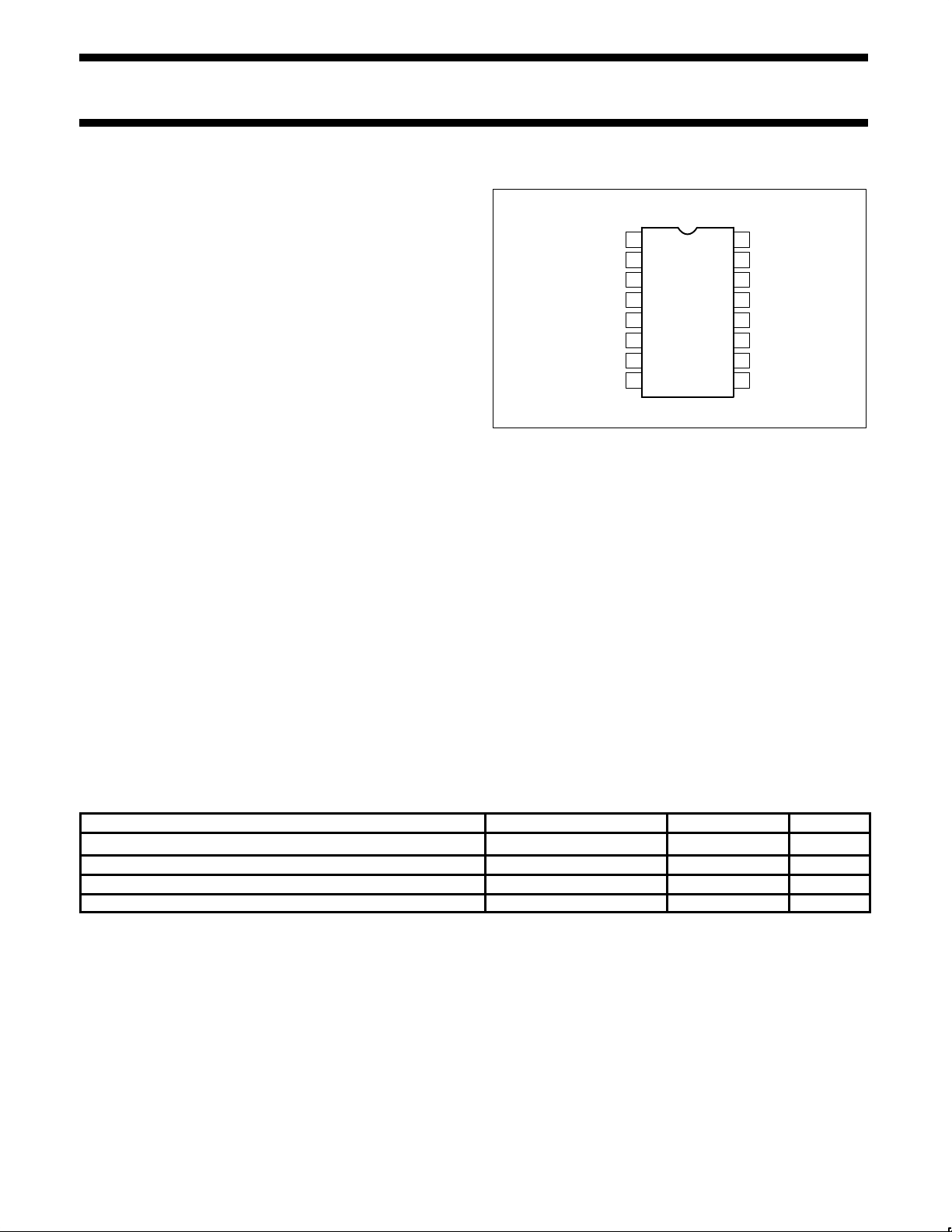
PIN CONFIGURA TION
N, D PACKAGES
1
V
CC1
2
GND
1
3
IN
A
4
GND
1
5
IN
B
6
GND
1
7
V
BG
8
V
AGC
Figure 1. Pin Configuration
APPLICATIONS
•Linear AGC systems
•Very linear AM modulator
•RF balun
•Cable TV multi-purpose amplifier
•Fiber optic AGC
•RADAR
•User programmable fixed gain block
•Video
•Satellite receivers
•Cellular communications
16
V
CC2
15
GND
2
14
OUT
A
13
GND
2
12
OUT
B
11
GND
2
10
GND
2
9
GND
2
SR00237
ORDERING INFORMATION
DESCRIPTION TEMPERATURE RANGE ORDER CODE DWG #
16-Pin Plastic Small Outline (SO) package
16-Pin Plastic Dual In-Line Package (DIP) 0 to +70°C NE5209N SOT28-4
16-Pin Plastic Small Outline (SO) package -40 to +85°C SA5209D SOT109-1
16-Pin Plastic Dual In-Line Package (DIP) -40 to +85°C SA5209N SOT28-4
1990 Aug 20 853-1453 00223
2
0 to +70°C
NE5209D SOT109-1
Page 3
Philips Semiconductors Product specification
SYMBOL
PARAMETER
TEST CONDITIONS
UNIT
ICCS
t
A
AVVolt
t)
dB
AVVolt
/diff
t)
dB
RINInput resistance (single-ended)
kΩ
R
Output resistance (single-ended)
Ω
VOSOutput offset voltage (output referred)
mV
VINDC level on inputs
V
V
DC level on outputs
V
PSRR
dB
BG
gp g
NE/SA5209Wideband variable gain amplifier
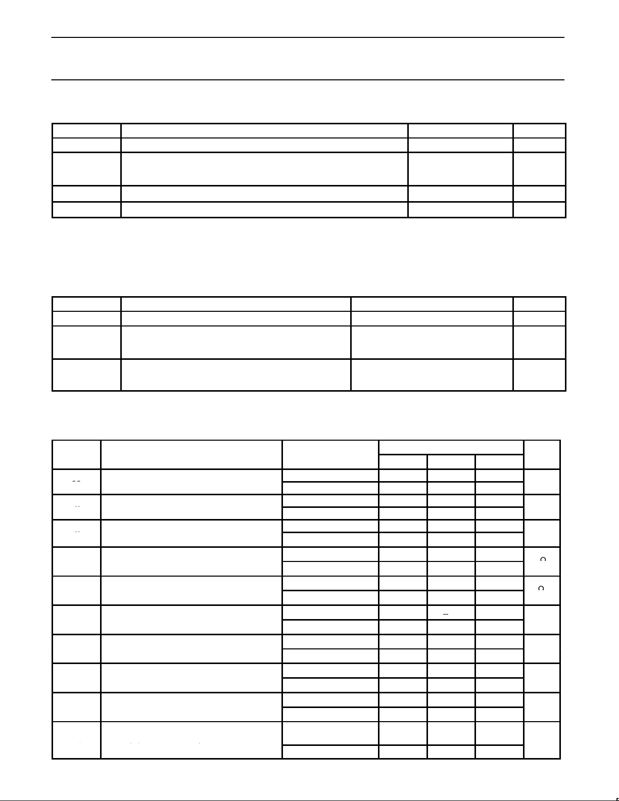
ABSOLUTE MAXIMUM RATINGS
SYMBOL PARAMETER RATING UNITS
V
CC
P
D
T
JMAX
T
STG
NOTES:
1. Maximum dissipation is determined by the operating ambient temperature and the thermal resistance, θ
16-Pin DIP: θ
16-Pin SO: θ
RECOMMENDED OPERATING CONDITIONS
SYMBOL PARAMETER RATING UNITS
V
CC
T
A
T
J
Supply voltage -0.5 to +8.0 V
Power dissipation, TA = 25oC (still air)
16-Pin Plastic DIP
16-Pin Plastic SO
1
1450
1100
mW
mW
Maximum operating junction temperature 150
Storage temperature range -65 to +150
:
= 85°C/W
JA
= 110°C/W
JA
Supply voltage V
CC1
JA
= V
= 4.5 to 7.0V V
CC2
Operating ambient temperature range
NE Grade
SA Grade
0 to +70
-40 to +85
Operating junction temperature range
NE Grade
SA Grade
0 to +90
-40 to +105
°C
°C
°C
°C
°C
°C
DC ELECTRICAL CHARACTERISTICS
TA = 25oC, V
OUT
OUT
V
BG
CC1
= V
CC2
= +5V, V
= 1.0V , unless otherwise specified.
AGC
upply curren
age gain (single-ended in/single-ended ou
age gain (single-ended in
-
-
Output offset supply rejection ratio
(output referred)
Bandgap reference voltage
erential ou
LIMITS
MIN TYP MAX
DC tested 38 43 48
Over temperature
1
30 55
DC tested, RL = 10kΩ 17 19 21
Over temperature
1
16 22
DC tested, RL = 10kΩ 23 25 27
Over temperature
1
22 28
DC tested at ±50µA 0.9 1.2 1.5
Over temperature
1
0.8 1.7
DC tested at ±1mA 40 60 75
Over temperature
1
35 90
+20 ±100
Over temperature
1
±250
1.6 2.0 2.4
Over temperature
1
1.4 2.6
1.9 2.4 2.9
Over temperature
1
1.7 3.1
20 45
Over temperature
4.5V<VCC<7V
= 10kΩ
R
BG
Over temperature
1
15
1.2 1.32 1.45
1
1.1 1.55
m
V
1990 Aug 20
3
Page 4
Philips Semiconductors Product specification
SYMBOL
PARAMETER
TEST CONDITIONS
UNIT
I
AGC pin DC bias current
A
SYMBOL
PARAMETER
TEST CONDITIONS
UNIT
BW-3dB bandwidth
MHz
GF
Gain flatness
dB
V
NE/SA5209Wideband variable gain amplifier
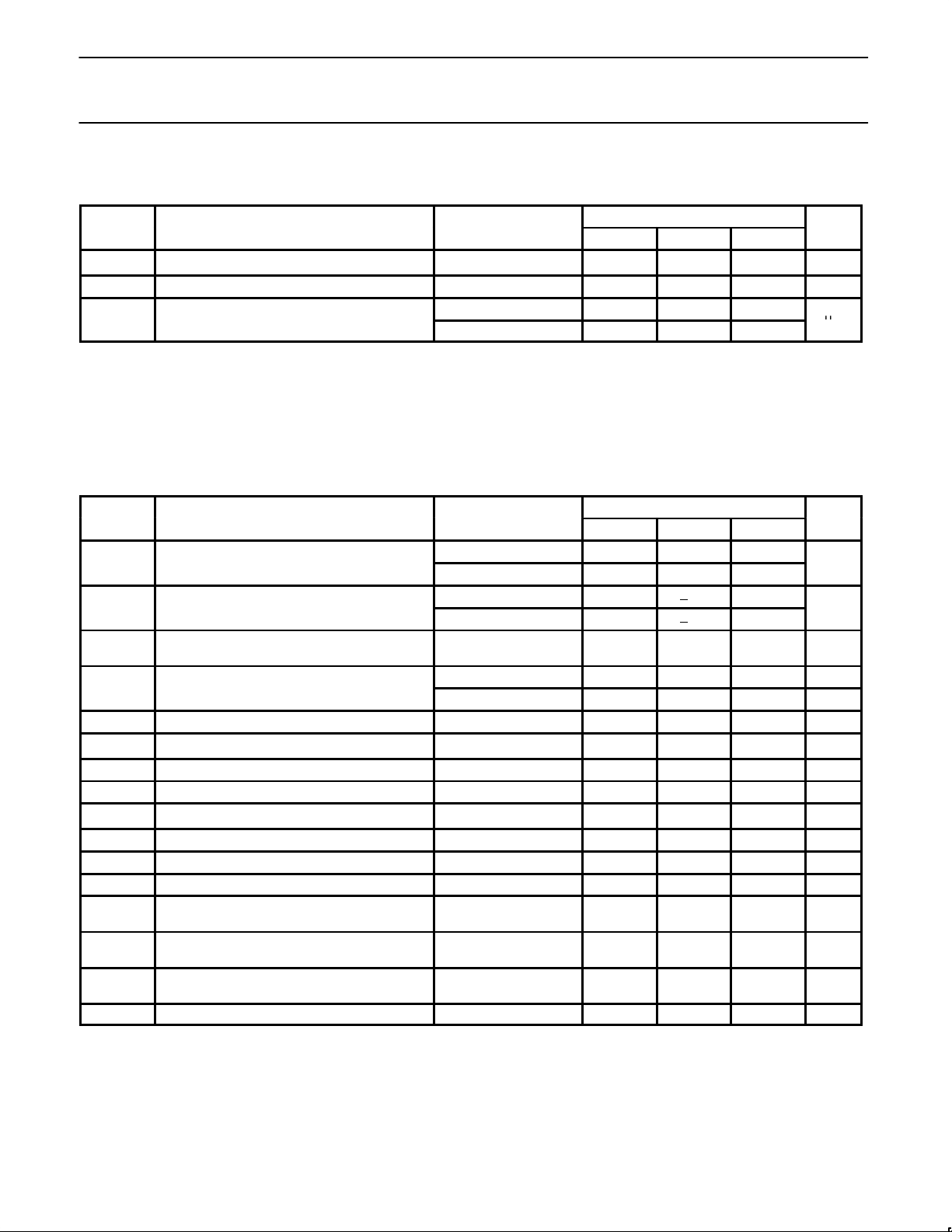
DC ELECTRICAL CHARACTERISTICS
TA = 25oC, V
R
BG
V
AGC
BAGC
NOTES:
1. “Over Temperature Range” testing is as follows:
At the time of this data sheet release, the D package over-temperature data sheet limits are guaranteed via guardbanded room temperature
testing only.
AC ELECTRICAL CHARACTERISTICS
TA = 25oC, V
V
IMAX
OMAX
NF Noise figure (unmatched configuration) RS = 50Ω, f = 50MHz 9.3 dB
V
IN-EQ
S12 Reverse isolation f = 100MHz -60 dB
∆G/∆V
∆G/∆T Gain temperature sensitivity RL = 50Ω 0.013
C
IN
BW
AGC
P
O-1dB
P
I-1dB
IP3
OUT
IP3
IN
∆G
AB
NOTE:
1. “Over Temperature Range” testing is as follows:
At the time of this data sheet release, the D package over-temperature data sheet limits are guaranteed via guardbanded room temperature
testing only.
2. With R
occurs at input for single-ended gain < 6dB and at output for single-ended gain > 6dB.
= V
CC1
= +5.0V, V
CC2
= 1.0V , unless otherwise specified.
AGC
LIMITS
MIN TYP MAX
Bandgap loading Over temperature
AGC DC control voltage range Over temperature
0V<V
AGC
Over temperature
1
1
2 10
0-1.3 V
<1.3V -0.7 -6
1
-10
NE is 0 to +70°C
SA is -40 to +85°C
= V
CC1
= +5.0V, V
CC2
= 1.0V , unless otherwise specified.
AGC
LIMITS
MIN TYP MAX
Over temperature
1
600 850
500
DC - 500MHz +0.4
Over temperature
Maximum input voltage swing (single-ended) for
linear operation
Maximum output voltage swing (single-ended)
for linear operation
2
RL = 50Ω 400 mV
2
RL = 1kΩ 1.9 V
Equivalent input noise voltage spectral density f = 100MHz 2.5
Gain supply sensitivity (single-ended) 0.3 dB/V
CC
1
+0.6
200 mV
nV/√Hz
dB/°C
Input capacitance (single-ended) 2 pF
-3dB bandwidth of gain control function 20 MHz
1dB gain compression point at output f = 100MHz -3 dBm
1dB gain compression point at input
Third-order intercept point at output
Third-order intercept point at input
f = 100MHz, V
f = 100MHz, V
f = 100MHz, V
Gain match output A to output B f = 100MHz, V
=0.1V
>0.5V
<0.5V
AGC
AGC
AGC
= 1V 0.1 dB
AGC
-10 dBm
+13 dBm
+5 dBm
NE is 0 to +70°C
SA is -40 to +85°C
> 1kΩ, overload occurs at input for single-ended gain < 13dB and at output for single-ended gain > 13dB. With RL = 50Ω, overload
L
kΩ
µ
P-P
P-P
P-P
1990 Aug 20
4
Page 5
Philips Semiconductors Product specification
NE/SA5209Wideband variable gain amplifier
NE5209 APPLICATIONS
The NE5209 is a wideband variable gain amplifier (VGA) circuit
which finds many applications in the RF, IF and video signal
processing areas. This application note describes the operation of
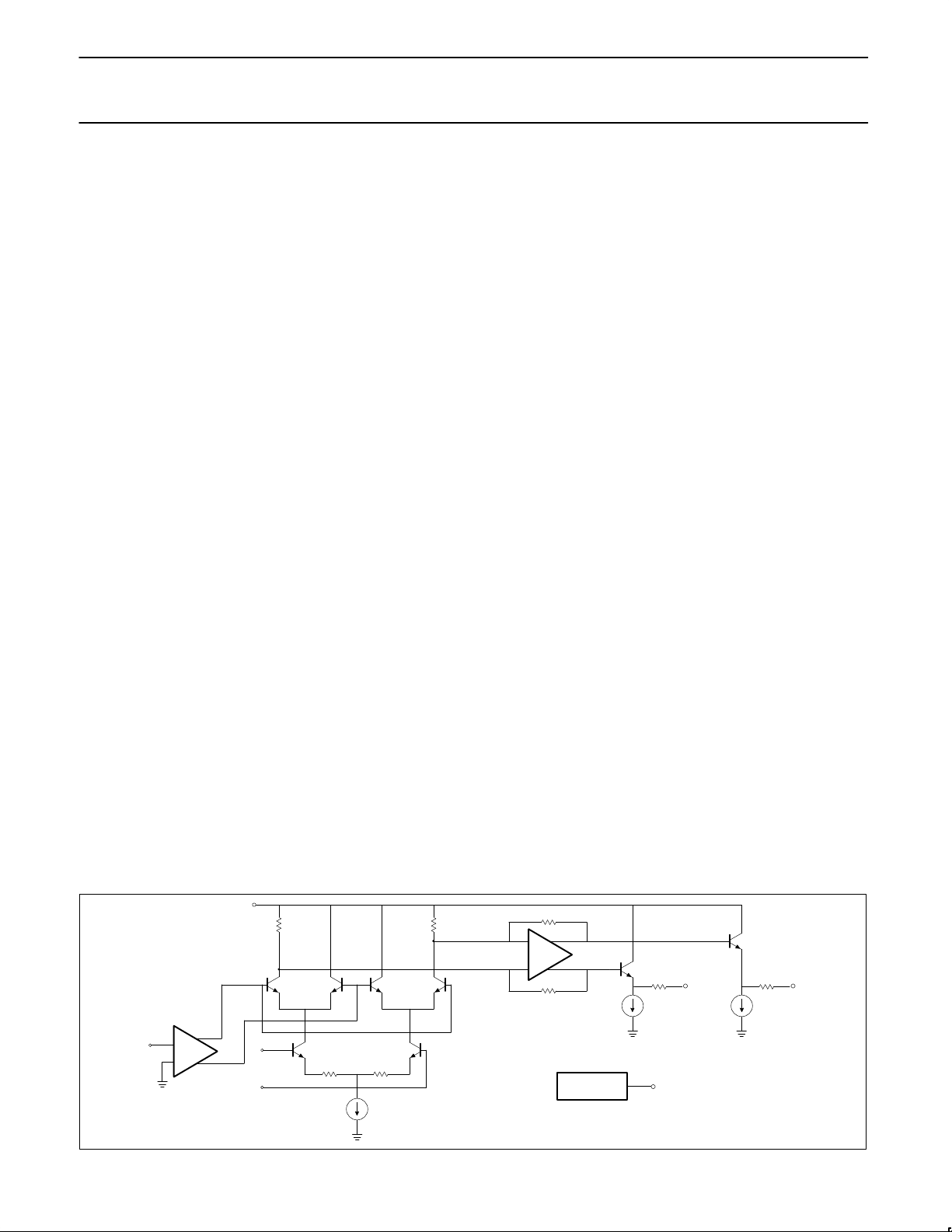
the circuit and several applications of the VGA. The simplified
equivalent schematic of the VGA is shown in Figure 2. Transistors
Q1-Q6 form the wideband Gilbert multiplier input stage which is
biased by current source I1. The top differential pairs are biased
from a buffered and level-shifted signal derived from the V
and the RF input appears at the lower differential pair. The circuit
topology and layout offer low input noise and wide bandwidth. The
second stage is a differential transimpedance stage with current
feedback which maintains the wide bandwidth of the input stage.
The output stage is a pair of emitter followers with 50Ω output
impedance. There is also an on-chip bandgap reference with
buffered output at 1.3V, which can be used to derive the gain control
voltage.
Both the inputs and outputs should be capacitor coupled or DC
isolated from the signal sources and loads. Furthermore, the two
inputs should be DC isolated from each other and the two outputs
should likewise be DC isolated from each other. The NE5209 was
designed to provide optimum performance from a 5V power source.
However, there is some range around this value (4.5 - 7V) that can
be used.
The input impedance is about 1kΩ. The main advantage to a
differential input configuration is to provide the balun function.
Otherwise, there is an advantage to common mode rejection, a
specification that is not normally important to RF designs. The
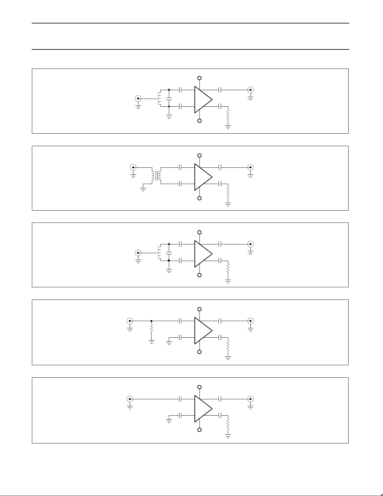
source impedance can be chosen for two different performance
characteristics: Gain, or noise performance. Gain optimization will
be realized if the input impedance is matched to about 1kΩ. A 4:1
balun will provide such a broadband match from a 50Ω source.
Noise performance will be optimized if the input impedance is
matched to about 200Ω. A 2:1 balun will provide such a broadband
match from a 50Ω source. The minimum noise figure can then be
expected to be about 7dB. Maximum gain will be about 23dB for a
single-ended output. If the differential output is used and properly
matched, nearly 30dB can be realized. With gain optimization, the
noise figure will degrade to about 8dB. With no matching unit at the
input, a 9dB noise figure can be expected from a 50Ω source. If the
source is terminated, the noise figure will increase to about 15dB.
All these noise figures will occur at maximum gain.
The NE5209 has an excellent noise figure vs gain relationship. With
any VGA circuit, the noise performance will degrade with decreasing
AGC
input
gain. The 5209 has about a 1.2dB noise figure degradation for
each 2dB gain reduction. With the input matched for optimum gain,
the 8dB noise figure at 23dB gain will degrade to about a 20dB
noise figure at 0dB gain.
The NE5209 also displays excellent linearity between voltage gain
and control voltage. Indeed, the relationship is of sufficient linearity
that high fidelity AM modulation is possible using the NE5209. A
maximum control voltage frequency of about 20MHz permits video
baseband sources for AM.
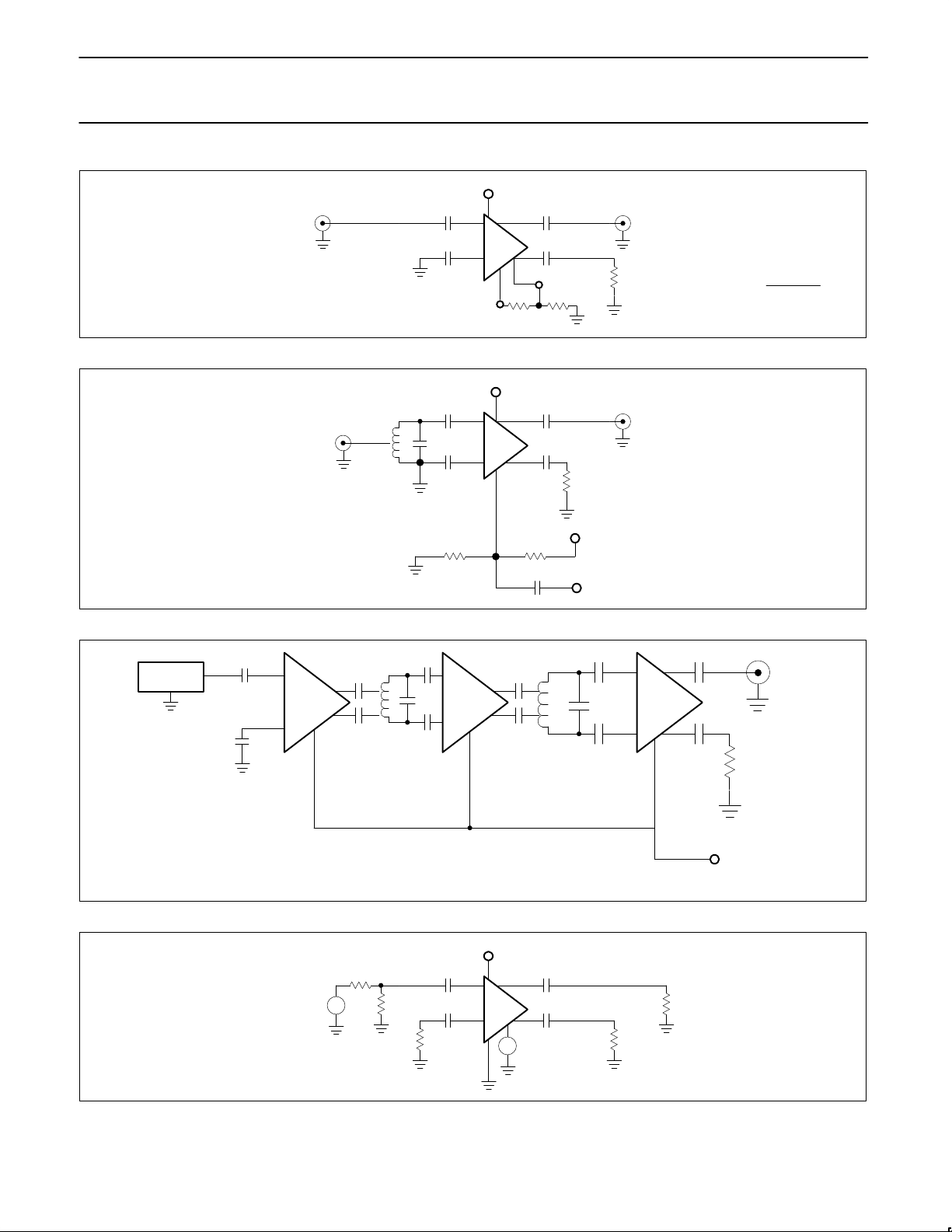
A stabilized bandgap reference voltage is made available on the
NE5209 (Pin 7). For fixed gain applications this voltage can be
resistor divided, and then fed to the gain control terminal (Pin 8).
Using the bandgap voltage reference for gain control produces very
stable gain characteristics over wide temperature ranges. The gain
setting resistors are not part of the RF signal path, and thus stray
capacitance here is not important.
The wide bandwidth and excellent gain control linearity make the
NE5209 VGA ideally suited for the automatic gain control (AGC)
function in RF and IF processing in cellular radio base stations,
Direct Broadcast Satellite (DBS) decoders, cable TV systems, fiber
optic receivers for wideband data and video, and other radio
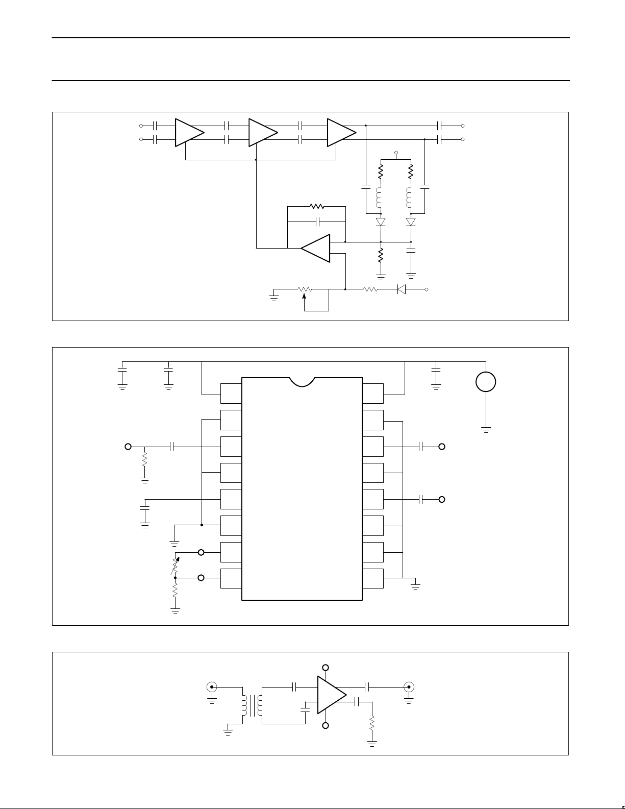
communication applications. A typical AGC configuration using the
NE5209 is shown in Figure 3. Three NE5209s are cascaded with
appropriate AC coupling capacitors. The output of the final stage
drives the full-wave rectifier composed of two UHF Schottky diodes
BAT17 as shown. The diodes are biased by R1 and R2 to V
CC
such
that a quiescent current of about 2mA in each leg is achieved. An
NE5230 low voltage op amp is used as an integrator which drives
the V
pin on all three NE5209s. R3 and C3 filter the high
AGC
frequency ripple from the full-wave rectified signal. A voltage
divider is used to generate the reference for the non-inverting input
of the op amp at about 1.7V. Keeping D3 the same type as D1 and
D2 will provide a first order compensation for the change in Schottky
voltage over the operating temperature range and improve the AGC
performance. R6 is a variable resistor for adjustments to the op
amp reference voltage. In low cost and large volume applications
this could be replaced with a fixed resistor, which would result in a
slight loss of the AGC dynamic range. Cascading three NE5209s
will give a dynamic range in excess of 60dB.
The NE5209 is a very user-friendly part and will not oscillate in most
applications. However, in an application such as with gains in
excess of 60dB and bandwidth beyond 100MHz, good PC board
layout with proper supply decoupling is strongly recommended.
V
0–1V
1990 Aug 20
AGC
V
CC
R
1
Q
Q
1
2
+
–
IN
Q
5
B
IN
A
I
1
Q
3
R
2
Q
4
Q
6
R
3
A1
R
4
BANDGAP
REFERENCE
Q
7
Q
8
I
2
OUT
B
Ω
50
I
3
V
BG
OUT
A
Ω
50
SR00238
Figure 2. Equivalent Schematic of the VGA
5
Page 6
Philips Semiconductors Product specification
NE/SA5209Wideband variable gain amplifier
RF/IF
INPUT
R1=R2= 3.9k
2πfL1= 10k
L
1
= 360Ω
R
3
R
= 62k
4
= 100Ω
R
5
= 1k pot
R
6
=L
2
10µF
5209 5209
5209
R4
C4
–
5230
+
R6
Figure 3. AGC Configuration Using Cascaded NE5209s
0.1µF
1
V
CC1
2
GND1
V
CC2
GND
2
V
CC
R1
R2
L1 L2
D1 D2
BAT 17
C3
R3
D3
R5
BAT 17
16
15
AGC
OUTPUT
V
CC
SR00239
0.1µF
+
V
CC
V
5VDC
V
IN
50Ω
0.1µF
0.1µF
IN
3
A
4
GND1
IN
5
B
GND1
6
7
V
BG
V
8
AGC
(16-Pin SO, 150-mil wide)
OUT
GND2
OUT
GND2
GND2
GND2
14
A
13
12
B
11
10
9
0.1µF
0.1µF
OUT
OUT
A
B
SR00240
Figure 4. VGA AC Evaluation Board
+5V
5209
+1V
V
AGC
50Ω
50Ω
OUTPUT
This circuit will exhibit about a 7dB
noise figure with approximately
22dB gain.
SR00241
50Ω
SOURCE
MINI CIRCUITS
2:1 BALUN
OR SIMILAR
1 : 2
Figure 5. Broadband Noise Optimization
1990 Aug 20
6
Page 7
Philips Semiconductors Product specification
NE/SA5209Wideband variable gain amplifier
50Ω
SOURCE
50Ω
SOURCE
50Ω
SOURCE
2:1 TURNS RATIO
LC TUNED
TRANSFORMER
+5V
5209
+1V
V
AGC
50Ω
Figure 6. Narrowband Noise Optimization
MINI CIRCUITS
4:1 BALUN OR
EQUIVALENT
1 : 4
+5V
5209
+1V
V
50Ω
AGC
Figure 7. Broadband Gain Optimization
4:1 TURNS RATIO
LC TUNED
TRANSFORMER
+5V
5209
+1V
V
AGC
50Ω
Figure 8. Narrowband Gain Optimization
50Ω
OUTPUT
50Ω
OUTPUT
50Ω
OUTPUT
This circuit will exhibit about a 7dB
noise figure with approximately
22dB gain. Narrowband circuits
have the advantage of greater stability, particularly when multiple devices are cascaded.
SR00242
This circuit will exhibit about an 8dB
noise figure with 24dB gain.
SR00243
This circuit will exhibit approximately an 8dB noise figure and 25dB gain.
SR00244
1990 Aug 20
50Ω
SOURCE
50Ω
SOURCE
+5V
50Ω
5209
+1V
V
AGC
50Ω
Figure 9. Simple Amplifier Configuration
+5V
5209
50Ω
V
AGC
+1V
Figure 10. Unterminated Configuration
7
50Ω
OUTPUT
50Ω
OUTPUT
The noise figure of this configuration
will be approximately 15dB.
SR00245
With the 50Ω source left unterminated, the noise figure is 9dB.
SR00246
Page 8
Philips Semiconductors Product specification
NE/SA5209Wideband variable gain amplifier
+5V
50Ω
SOURCE
RF INPUT
SOURCE
5209
V
AGC
V
BG
R
R
1
Figure 11. User-Programmable Fixed Gain Block
+5V
50Ω
5209
V
AGC
.5V
R9R
Figure 12. AM Modulator
2
50Ω
50Ω
OUTPUT
50Ω
FULL CARRIER
AM (DSB)
50Ω
OUTPUT
+5V
MODULATING
SIGNAL
Gain = 19dB + 20log10 V
AGC
=
R1 R
where V
and is in units of Volts, for V
All harmonic distortion products will be
at least -50dBc over the audio spectrum.
AGC
R
2
2
AGC
SR00247
SR00248
V
≤ 1V
BG
CRYSTAL
FILTER
V
AGC
The high input impedance to the NE5209 makes matching
to crystal filters relatively easy. The total delta gain of this
system will approach 80dB. IF frequencies well into the UHF
region can be configured with this type of architecture.
±
V
S
Figure 14. Test Set-up 1 (Used for all Graphs)
52095209
V
AGC
Figure 13. Receiver AGC IF Gain
V
CC
R
S
R
T
R
T
5209
±
(+5V, unless otherwise noted)
R
V
AGC
L
5209
V
AGC
R
50Ω
OUTPUT
50Ω
GAIN CONTROL
SIGNAL
SR00249
L
SR00250
1990 Aug 20
8
Page 9
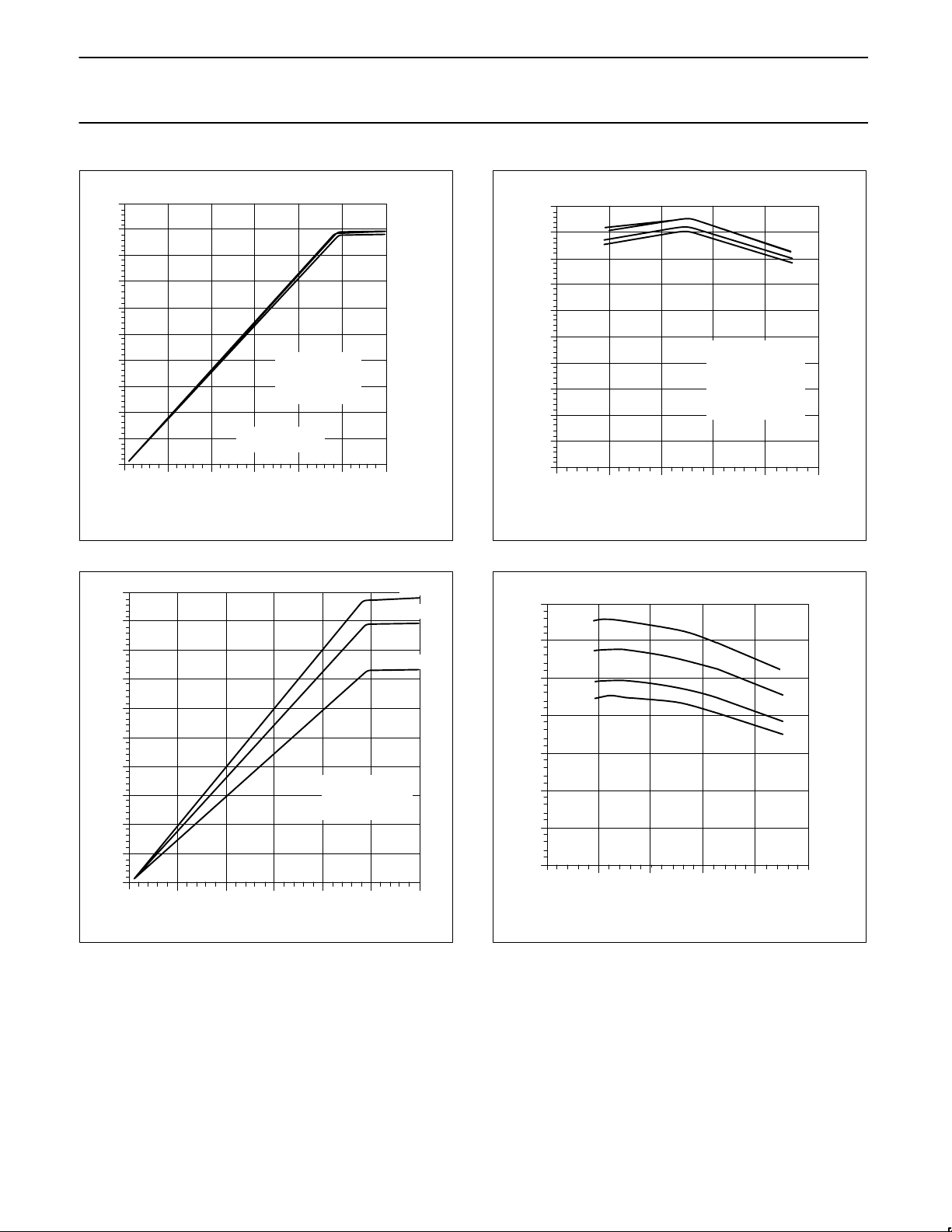
Philips Semiconductors Product specification
NE/SA5209Wideband variable gain amplifier
10
9
8
7
6
5
4
21
S Magnitude
3
2
1
0
0 0.6 10.80.40.2
DC Tested
See test-setup 1
V
AGC
Figure 15. Gain vs V
10
9
8
7
6
5
4
21
S Magnitude
3
2
1
0
0 0.2 0.4 0.6 0.8
V
AGC
Figure 16. Insertion Gain vs V
T = 25°C
= RL = 50Ω
R
S
= ∞
R
t
f = 10MHz
(V)
and V
AGC
(V)
and Temperature
AGC
1.2
CC
RS = RL = 50Ω
= ∞
R
t
See test-setup 1
1 1.2
V
CC
V
CC
V
CC
SR00251
-55°C
+25°C
+125°C
SR00253
= 5.5V
= 5.0V
= 4.5V
20
19.5
19
18.5
18
17.5
17
16.5
Differential Voltage Gain (dB)
16
15.5
15
–100 50 1501000–50
Temperature (°C)
RS = 0Ω
= ∞
R
L
Rt = ∞
V
= 1.1V
AGC
See Test Setup 1
Figure 17. Voltage Gain vs Temperature and V
55
50
45
40
35
Supply Current (mA)
30
25
See test-setup 1
20
–100 –50 0 50 100
Temperature (°C)
Figure 18. Supply Current vs Temperature and V
5.5V
5.0V
4.5V
SR00252
CC
VCC = 7.0V
VCC = 6.0V
VCC = 5.0V
VCC = 4.5V
150
SR00254
CC
1990 Aug 20
9
Page 10
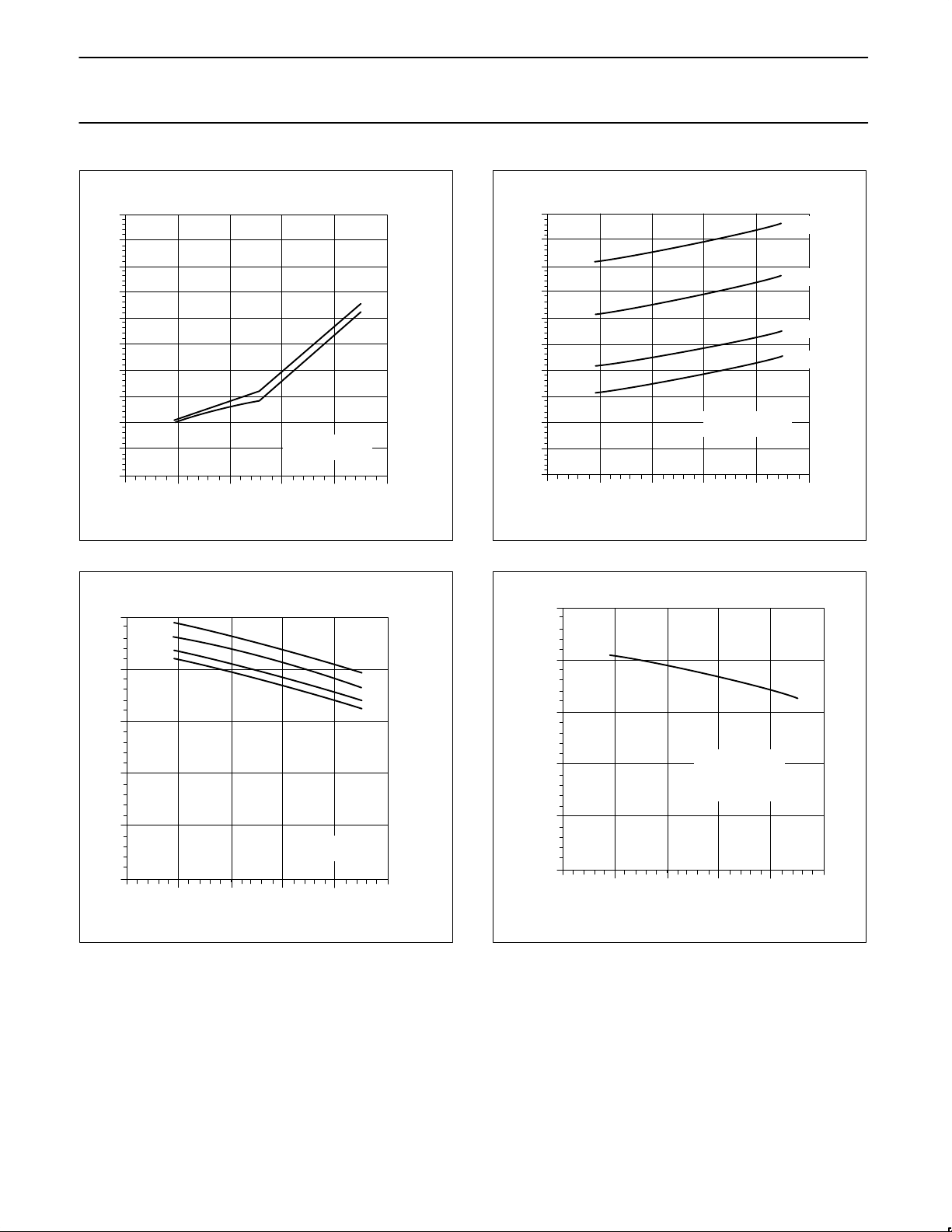
Philips Semiconductors Product specification
NE/SA5209Wideband variable gain amplifier
1.5
1.45
1.4
1.35
1.3
1.25
1.2
1.15
Input Resistance (k )Ω
1.1
1.05
1
–100 –50 0 150100
Temperature (°C)
See test-setup 1
50
Figure 19. Input Resistance vs Temperature
2.5
2
1.5
DC Tested
= 7.0V
V
CC
V
= 4.5V
CC
SR00255
V
= 7.0V
CC
= 6.0V
V
CC
V
= 5.0V
CC
= 4.5V
V
CC
5
4.5
4
3.5
3
2.5
2
Output DC Voltage
1.5
1
0.5
0
–100 50 1501000–50
Temperature (°C)
DC Tested
See test-setup 1
VCC = 7.0V
VCC = 6.0V
VCC = 5.0V
VCC = 4.5V
Figure 21. Output Bias Voltage vs Temperature and V
2.5
2
1.5
SR00256
CC
1
Input Bias Voltage (V)
0.5
0
–100 50 150100
0–50
Temperature (°C)
Figure 20. Input Bias Voltage vs Temperature
1990 Aug 20
DC Tested
See test-setup 1
SR00257
10
V
= 1.1V
1
DC OUTPUT SWING (V)
0.5
0
–100 –50 150
0 50 100
Temperature (°C)
AGC
= 10kΩ
R
L
DC Tested
See test-setup 1
Figure 22. DC Output Swing vs Temperature
SR00258
Page 11
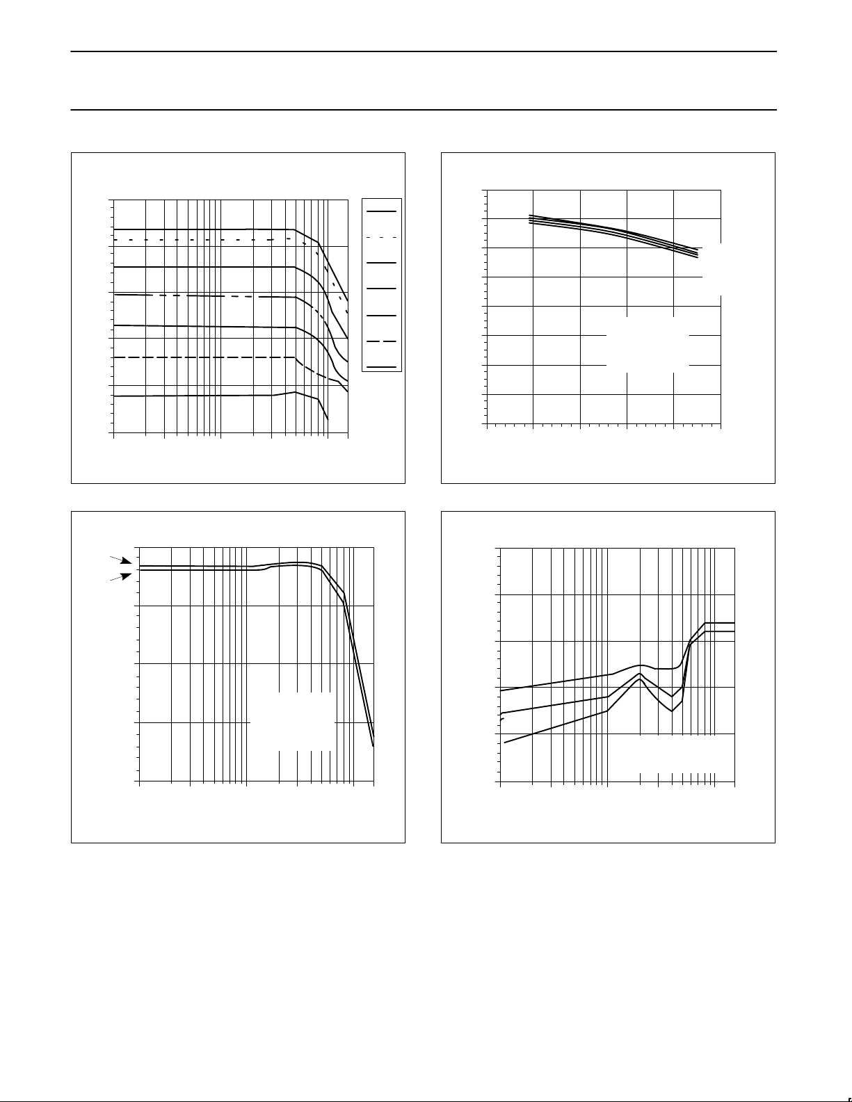
Philips Semiconductors Product specification
NE/SA5209Wideband variable gain amplifier
20
10
0
–10
21
S Magnitude (dB)
–20
–30
10 1500100
Frequency (MHz)
Figure 23. Insertion Gain vs Frequency and V
15
5.5V
4.5V
10
1000
T = 25°C
R
S
R
See Test
Setup 1
SR00259
AGC
1.1V
0.8V
0.4V
200mV
100mV
50mV
25mV
= RL =
50Ω
= 50Ω
t
16
14
12
10
8
T = 25°C
= 1.1V
6
21
S Magnitude (dB)
4
2
0
–100
0–50
Temperature (°C)
V
AGC
= 50Ω
R
t
f = 10MHz
See Test Setup 1
50
Figure 25. Insertion Gain vs Temperature and V
0
–5
VCC = 7.0V
= 6.0V
V
CC
V
= 5.0V
CC
= 4.5V
V
CC
150100
SR00260
CC
5
21
S Magnitude (dB)
0
–5
10
Frequency (MHz)
V
AGC
R
S
See Test Setup 1
100
T = 25°C
= 1.1V
= RL = 50Ω
R
= 50Ω
t
Figure 24. Insertion Gain vs Frequency and V
15001000
SR00261
CC
–10
22
125°C
S (dB)
–15
25°C
-55°C
–20
–25
10
100
Frequency (MHz)
RS = RL = 50Ω
= 50Ω
R
t
See Test Setup 1
Figure 26. Output Return Loss vs Frequency
15001000
SR00262
1990 Aug 20
11
Page 12
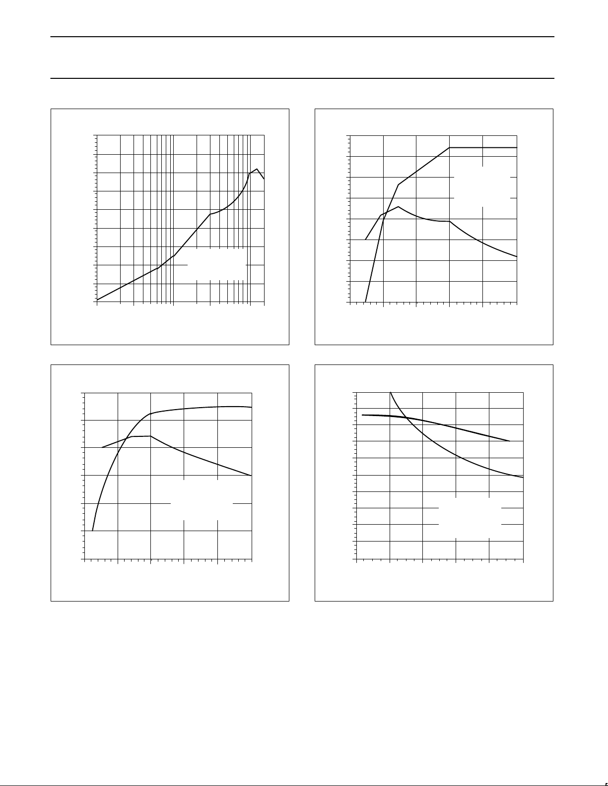
Philips Semiconductors Product specification
NE/SA5209Wideband variable gain amplifier
0
–10
–20
–30
–40
–50
12
S Magnitude (dB)
–60
R
–70
–80
–90
10
Frequency (MHz)
S
See test-setup 1
100
Figure 27. Reverse Isolation vs Frequency
0
–5
–10
–15
–1
P (dBm)
–20
–25
–30
0 0.2 1
0.4 0.6 0.8
V
AGC
T = 25°C
= RL = 50Ω
R
S
= 50Ω
R
t
f = 100MHz
See test-setup 1
(V)
Figure 28. 1dB Gain Compression vs V
T = 25°C
= RL = 50Ω
Rt = 50Ω
AGC
1500
1000
SR00263
OUTPUT
INPUT
SR00265
15
10
5
3
IM Intercept (dBm)
0
–5
0 0.2 0.4 0.6 0.8
V
AGC
(V)
T = 25°C
= RL = 50Ω
R
S
= 50Ω
R
t
f = 100MHz
See test-setup 1
1
SR00264
Figure 29. Third-Order Intermodulation Intercept vs V
20
18
16
14
12
10
NF (dB)
8
6
4
2
0
0 0.2 1
0.4 0.6 0.8
V
Figure 30. Noise Figure vs V
See test-setup 1
(V)
AGC
T = 25°C
= RL = 50Ω
R
S
R
t
f = 50MHz
= ∞
SR00266
AGC
OUTPUT
INPUT
AGC
1990 Aug 20
12
Page 13
Philips Semiconductors Product specification
NE/SA5209Wideband variable gain amplifier
16
14
12
10
8
NF (dB)
6
4
2
0
10 100 1000
0Ω Termination
on INB
50Ω Termination
on INB
Frequency (MHz)
T = 25°C
= 1.1V
V
AGC
= RL = 50Ω
R
S
Rt = ∞ on INA
See test-setup 1
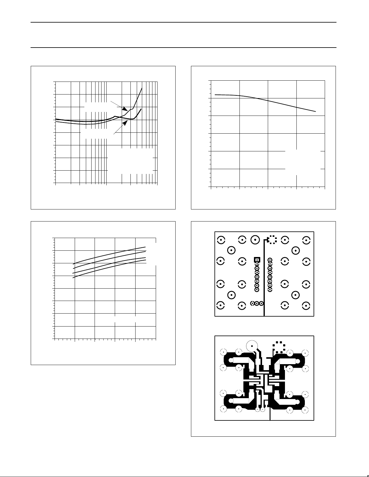
Figure 31. Noise Figure vs Frequency
1.4
1.35
1.3
1.25
SR00267
VCC = 7.0V
= 6.0V
V
CC
VCC = 5.0V
= 4.5V
V
CC
12
10
8
6
21
S Magnitude (dB)
4
2
0
–60 –10 40 90 140
Temperature (°C)
RS = RL = 50Ω
= 50Ω
R
t
R
= R2 = 10k
1
f = 100MHz
See Figure 10
Figure 33. Fixed Gain vs Temperature
+V
GND
CC
IN
A
OUT
A
SR00268
1.2
1.15
Bandgap Voltage (V)
1.1
1.05
1
–100
Temperature (°C)
0–50
Bandgap Load = 2kΩ
50
Figure 32. Bandgap Voltage vs Temperature and V
150100
SR00269
CC
IN
GND
AGC
VBG
B
NE5209
OUT
B
TOP VIEW - COMPONENT SIDE
TOP VIEW - SOLDER SIDE
Figure 34. VGA AC Evaluation Board Layout
SR00270
1990 Aug 20
13
Page 14
Philips Semiconductors Product specification
NE/SA5209Wideband variable gain amplifier
IN
NE5209
IN
+V
CC
A
B
GND
OUT
OUT
A
B
TOP VIEW - COMPONENT SIDE
TOP VIEW - SOLDER SIDE
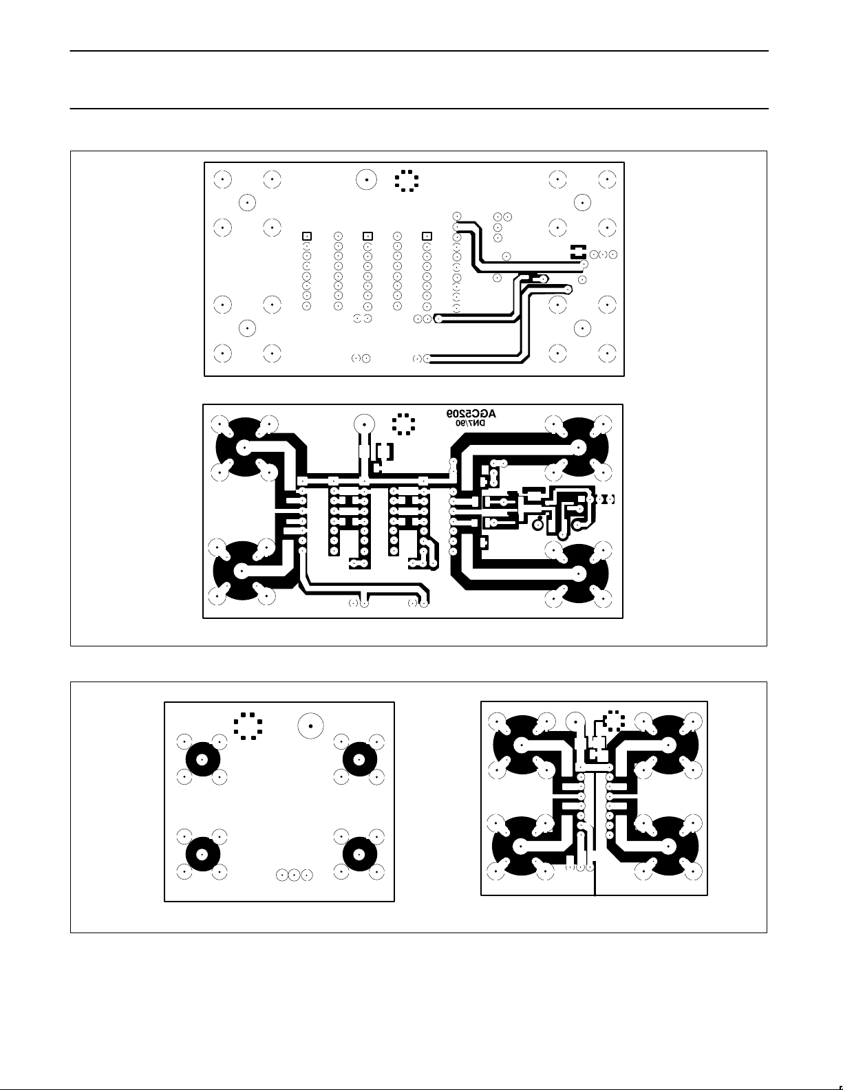
Figure 35. AGC Configuration Using Cascaded NE5209s - Layout
AMP10101 / NE5219SO/DN8.90
Figure 36. VGA AC Evaluation Board Layout (DIP Package)
SR00271
TOP VIEW - SOLDER SIDETOP VIEW - COMPONENT SIDE TOP VIEW - SOLDER SIDE
SR00272
1990 Aug 20
14
Page 15

Philips Semiconductors Product specification
NE/SA5209Wideband variable gain amplifier
DEFINITIONS
Data Sheet Identification Product Status Definition
Objective Specification
Preliminary Specification
Product Specification
Formative or in Design
Preproduction Product
Full Production
Philips Semiconductors and Philips Electronics North America Corporation reserve the right to make changes, without notice, in the products,
including circuits, standard cells, and/or software, described or contained herein in order to improve design and/or performance. Philips
Semiconductors assumes no responsibility or liability for the use of any of these products, conveys no license or title under any patent, copyright,
or mask work right to these products, and makes no representations or warranties that these products are free from patent, copyright, or mask
work right infringement, unless otherwise specified. Applications that are described herein for any of these products are for illustrative purposes
only. Philips Semiconductors makes no representation or warranty that such applications will be suitable for the specified use without further testing
or modification.
LIFE SUPPORT APPLICA TIONS
Philips Semiconductors and Philips Electronics North America Corporation Products are not designed for use in life support appliances, devices,
or systems where malfunction of a Philips Semiconductors and Philips Electronics North America Corporation Product can reasonably be expected
to result in a personal injury. Philips Semiconductors and Philips Electronics North America Corporation customers using or selling Philips
Semiconductors and Philips Electronics North America Corporation Products for use in such applications do so at their own risk and agree to fully
indemnify Philips Semiconductors and Philips Electronics North America Corporation for any damages resulting from such improper use or sale.
Philips Semiconductors
811 East Arques Avenue
P.O. Box 3409
Sunnyvale, California 94088–3409
Telephone 800-234-7381
This data sheet contains the design target or goal specifications for product development. Specifications
may change in any manner without notice.
This data sheet contains preliminary data, and supplementary data will be published at a later date. Philips
Semiconductors reserves the right to make changes at any time without notice in order to improve design
and supply the best possible product.
This data sheet contains Final Specifications. Philips Semiconductors reserves the right to make changes
at any time without notice, in order to improve design and supply the best possible product.
Philips Semiconductors and Philips Electronics North America Corporation
register eligible circuits under the Semiconductor Chip Protection Act.
Copyright Philips Electronics North America Corporation 1993
All rights reserved. Printed in U.S.A.
1990 Aug 20
15
 Loading...