

Philips SA2420DH Datasheet

INTEGRATED CIRCUITS
SA2420
Low voltage RF transceiver — 2.45GHz
Product specification 1997 May 23
Philips Semiconductors Product specification
SA2420Low voltage RF transceiver — 2.45 GHz
DESCRIPTION
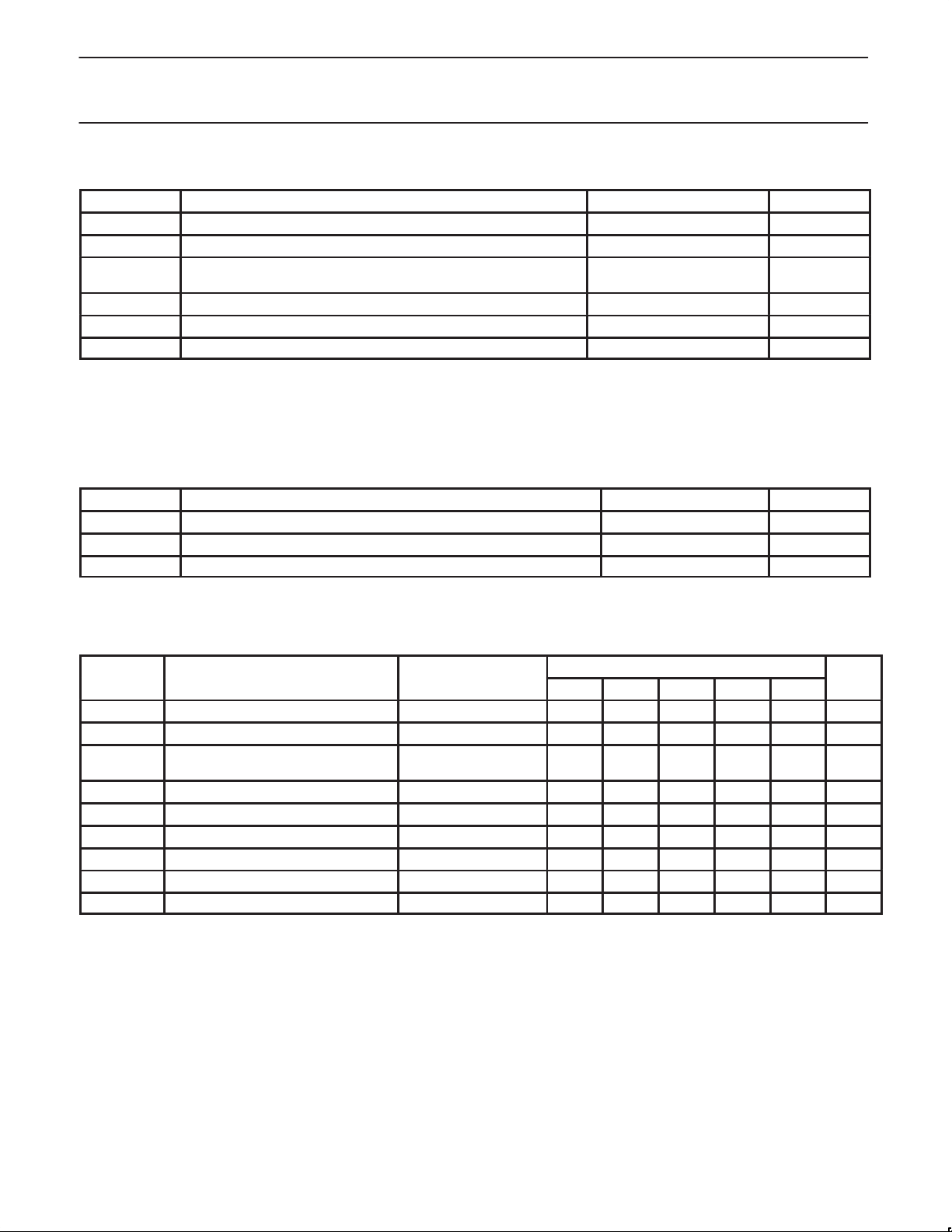
The SA2420 transceiver is a combined low-noise amplifier, receive
mixer, transmit mixer and LO buf fer IC designed for
high-performance low-power communication systems for
2.4-2.5GHz applications. The LNA has a 2.5dB noise figure at
2.45GHz with 14dB gain and an IP3 intercept of -3dBm at the input.
The gain is stabilized by on-chip compensation to vary less than
±0.2dB over the -40 to +85°C temperature range. The
wide-dynamic-range receive mixer has a 10.9dB noise figure and an
input IP3 of +2.8dBm at 2.45GHz. The nominal current drawn from
a single 3V supply is 37mA in transmit mode and 22mA in receive
mode.
FEATURES
•Low current consumption: 37mA nominal transmit mode and
22mA nominal receive mode
•Fabricated on a high volume, rugged BiCMOS technology
•High system power gain: 22.5dB (LNA + Mixer) at 2.45GHz
•TSSOP24 package
•Excellent gain stability versus temperature and supply voltage
•-10dBm LO input power can be used to drive the mixer
•Operates with either full or half frequency LO
•Wide IF range: 50–500MHz
ORDERING INFORMATION
DESCRIPTION TEMPERATURE RANGE ORDER CODE DWG #
24-Pin Plastic Thin Shrink Small Outline Package (Surface-mount, TSSOP)
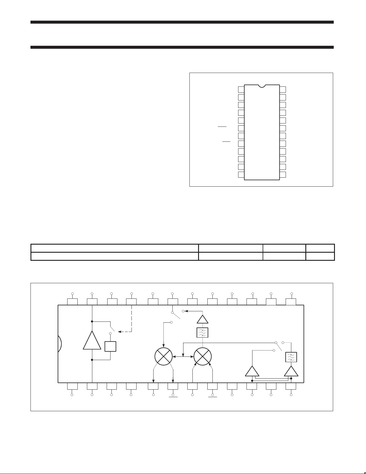
PIN CONFIGURATION
DH Package
GND
1
LNA IN
2
GND
3
4
GND
OUT
GND
LOP
LO SW
LOM
5
6
7
IN
8
9
10
11
12
Rx IF OUT
Rx IF
Tx IF IN
Tx IF
Figure 1. Pin Configuration
APPLICATIONS
•2.45GHz WLAN front-end (802.11, ISM)
-40 to +85°C
SA2420DH SOT355-1
24
V
LNA OUT
23
GND
22
ATTEN SW
21
GND
20
19
RF IN/OUT
GND
18
Tx/Rx SW
17
GND
16
GND
15
14
V
CHIP EN
13
SR00164
CC
CC
LO
BLOCK DIAGRAM
V
CC
24 23 22 21 20
GND GND
LNA
OUT
LNA
LNA
IN
GND
ATTENUATOR
ATTEN
SW
GND
RF IN/
OUT GND
GND
Tx/Rx
SW GND
19 18 17 16 15
TX
PRE-DRIVER
BPF
RX
RX TX
43215
GND
Rx IF
OUT
Rx IF
OUT
761098
Tx IFINTx IF
IN
Figure 2. SA2420 Block Diagram
BUFFER
V
LO
CHIP
CC
14 13
BPF
FREQ.
DBLER
1211
LOGND LOP
SW
LOM
EN
X2X1
SR00165
1997 May 23 853–1984 18069
2
Philips Semiconductors Product specification
SYMBOL
PARAMETER
TEST CONDITIONS
UNITS
SA2420Low voltage RF transceiver — 2.45 GHz
ABSOLUTE MAXIMUM RATINGS
SYMBOL PARAMETER RATING UNITS
V
CC
V
IN
P
D
T
JMAX
P
MAX
T
STG
NOTE:
1. Transients exceeding these conditions may damage the product.
2. Maximum dissipation is determined by the operating ambient temperature and the thermal resistance, and absolute maximum ratings may
impact product reliability θ
3. IC is protected for ESD voltages for 2000V , excepts pins 10 and 12, which are protected up to 500V.
RECOMMENDED OPERATING CONDITIONS
SYMBOL PARAMETER RATING UNITS
V
CC
T
A
T
J
Supply voltage -0.3 to +6 V
Voltage applied to any pin -0.3 to (VCC + 0.3) V
Power dissipation, TA = 25°C (still air)
24-Pin Plastic TSSOP
555
mW
Maximum operating junction temperature 150 °C
Maximum power (RF/IF/LO pins) +20 dBm
Storage temperature range –65 to +150 °C
: 24-Pin TSSOP = 117°C/W
JA
Supply voltage 2.7 to 5.5 V
Operating ambient temperature range -40 to +85 °C
Operating junction temperature -40 to +105 °C
DC ELECTRICAL CHARACTERISTICS
VCC = +3V, TA = 25°C; unless otherwise stated.
I
CCTX
I
CCRX
I
CC OFF
V
LNA-IN
I
LNA-OUT
V
LO 2.1 GHz
V
LO 1.05 GHz
V
TX IF
V
TX IFB
Supply current, Transmit LO mode = Hi 25 37 45 mA
Supply current, Receive LO mode = Hi 15 22 28 mA
Power down mode (Tx/Rx SW = Low)
LNA input voltage Receive mode 0.855 V
LNA output bias current Receive mode 4.0 mA
LO buffer DC input voltage LO mode = Hi 2.1 V
LO buffer DC input voltage LO mode = Low 2.1 V
Tx Mixer input voltage Transmit mode 1.7 V
Tx Mixer input voltage Transmit mode 1.7 V
LO mode = Hi,
LNA gain = Hi
LIMITS
MIN -4σ TYP +4σ MAX
0 10 µA
1997 May 23
3
Philips Semiconductors Product specification
SYMBOL
PARAMETER
TEST CONDITIONS
UNITS
SA2420Low voltage RF transceiver — 2.45 GHz
AC ELECTRICAL CHARACTERISTICS
VCC = +3V, TA = 25°C; LOIN = -10dBm @ 2.1GHz; fRF = 2.45GHz; unless otherwise stated.
LIMITS
MIN -4σ TYP +4σ MAX
Low Noise Amplifier (In = Pin 2; Out = 23)
S
∆S21/∆T Gain temperature sensitivity LNA gain = Hi -0.002 dB/°C
∆S21/∆VCCGain VCC drift LNA gain = Hi 0.3 dB/V
S
S
S
ISO Isolation: LO1 to LNA
P
-1dB
IP3 Amplifier input third order intercept
NF Amplifier noise figure (50Ω) LNA gain = Hi 2.3 2.5 2.7 dB
LNA High Overload Mode
S
∆S21/∆T Gain temperature sensitivity LNA gain = Low -0.01 dB/°C
∆S21/∆VCCGain VCC drift LNA gain = Low 0.3 dB/V
S
S
S
ISO Isolation: LO1 to LNA
P
-1dB
IP3 Amplifier input third order intercept
NF Amplifier noise figure (50Ω) LNA gain = Low 17 dB
Rx Mixer (RF = Pin 19, IF = Pins 5 and 6, LO = Pin 10 or 12, PLO = -10dBm)
PG
∆GC/∆T Gain temperature drift -0.016 dB/°C
∆GC/∆VCCGain VCC drift 0.34 dB/V
S
11–RF
NF
P
-1dB
IP3 Input third order intercept f1 - f2 = 1MHz 1.7 2.8 3.9 dBm
f
RF
f
Amplifier gain LNA gain = Hi 12.7 14.0 15.3 dB
21
Amplifier reverse isolation LNA gain = Hi -22 dB
12
Amplifier input match
11
Amplifier output match
22
1
1
IN
LNA gain = Hi -8 dB
LNA gain = Hi -8 dB
LO mode = Hi,
LNA gain = Hi
-45 dB
Amplifier input 1dB gain compression LNA gain = Hi -15 dBm
f1 - f2 = 1MHz,
LNA gain = Hi
Amplifier gain LNA gain = Low –14.0 -13.3 –12.0 dB
21
Amplifier reverse isolation LNA gain = Low -16 dB
12
Amplifier input match
11
Amplifier output match
22
1
1
IN
LNA gain = Low -8 dB
LNA gain = Low -8 dB
LO mode = Hi,
LNA gain = Low
-3 dBm
-45 dB
Amplifier input 1dB gain compression LNA gain = Low +6 dBm
f1 - f2 = 1MHz,
LNA gain = Low
Power conversion gain into 50Ω :
matched to 50W using external balun
C
circuitry.
Input match at RF (2.45GHz)
SSB noise figure (2.45GHz) (50Ω) 10.2 10.9 11.6 dB
M
1
fS = 2.45GHz,
fLO = 2.1GHz,
f
= 350MHz
IF
7.9 8.5 9.1 dB
17 dBm
-15 dB
Mixer input 1dB gain compression –11.4 -10.3 –9.2 dBm
RF frequency range
IF frequency range
IF
3
3
2.4 2.45 2.5 GHz
300 350 400 MHz
1997 May 23
4

Philips Semiconductors Product specification
SYMBOL
PARAMETER
TEST CONDITIONS
UNITS
SA2420Low voltage RF transceiver — 2.45 GHz
AC ELECTRICAL CHARACTERISTICS (continued)
LIMITS
MIN -4σ TYP +4σ MAX
Rx Mixer Spurious Components (PIN = P
P
P
RF-IF
LO-IF
RF feedthrough to IF CL = 2pF per side -35 dBc
LO feedthrough to IF CL = 2pF per side -35 dBc
Tx Mixer (RF = Pin 19, IF = Pins 7 and 8, LO = Pin 10 or 12, PLO = -10dBm)
PG
Power conversion gain: RL = 50Ω
C
RS = 50Ω
∆GC/∆T Gain temperature drift -0.032 dB/°C
∆GC/∆VCCGain voltage drift 0.4 dB/V
S
NF
P
11–RF
-1dB
Output match at RF (2.45GHz)
SSB noise figure (2.45GHz) (50Ω) 13.2 dB
M
Output 1dB gain compression 1.5 2.9 4.3 dBm
IP3 Output third order intercept f1 - f2 = 1MHz 10.1 +11.5 12.9 dBm
f
RF
f
RF frequency range
IF frequency range
IF
Tx Mixer Spurious Components (P
P
IF-RF
P
LO-RF
P
2LO-RF
P
IMAGE-RF
IF feedthrough to RF -29 dBc
LO feedthrough to RF -20 dBc
2*LO feedthrough to RF -25 dBc
Image feedthrough to RF -0 dBc
3
3
OUT
LO Buffer: Full and Half Frequency inputs
P
S
11-LO1
S
11-LO2
f
LO2G
f
LO1G
Switching
t
Rx-Tx
t
Tx-Rx
t
POWER UP
t
PWR DWN
LO drive level (see figure 16) -10 -7 5 dBm
LO
Mixer input match (LO = 2.1GHz) LO mode = Hi -10 dB
Mixer input match (LO = 1.05GHz) LO mode = Low -10 dB
LO2G frequency range
LO1G frequency range
2
3
3
Receive-to-transmit switching time 1 µs
Transmit-to-Receive switching time 1 µs
Chip enable time 1 µs
Chip disable time 1 µs
NOTES:
1. With simple external matching
2. With 50pF coupling capacitors on all RF and IF parts
3. This part has been optimized for the frequency range at 2.4–2.5 GHz. Operation outside this frequency range may yield performance other
than specified in this datasheet.
= P
-1dB
1
-1dB
)
fS = 2.45GHz,
fLO = 2.1GHz,
15.0 17 19.9 dB
fIF = 350MHz
-10 dB
2.4 2.45 2.5 GHz
300 350 400 MHz
)
LO mode = Hi 1.9 2.1 2.3 GHz
LO mode = Low 0.85 1.05 1.25 GHz
1997 May 23
5
 Loading...