

Page 1

INTEGRATED CIRCUITS
SA2411
+20 dBm single chip linear amplifier for WLAN
Product data 2003 Feb 07
Supersedes data of 2002 Jul 31
Page 2
Philips Semiconductors Product data
TYPE NUMBER
SA241 1+20 dBm single chip linear amplifier for WLAN
1. DESCRIPTION
The SA2411 is a linear power amplifier designed for WLAN application in the 2.4 GHz band. Together with the SA2400A the chips form a
complete 802.1 1b transceiver. The SA2411 is a Si power amplifier with integrated matching and power level detector .
2. FEATURES
•75 Ω + 25j Ω differential inputs, internally matched
•50 Ω single-ended output, internally matched
•15 dB gain block
•Power detector
•Bias adjust pin
•18% efficiency at 3 V
•RF matching for SA2400A
3. APPLICATIONS
•IEEE 802.11 and 802.11b radios
•Supports DSSS and CCK modulation
•Supports data rates: 1, 2, 5.5, and 11 Mbps
•2.45 GHz ISM band wireless communication devices
Table 1. Ordering information
PACKAGE
NAME DESCRIPTION VERSION
SA2411DH TSSOP16 plastic thin shrink small outline package; 16 leads; body width 4.4 mm SOT403-1
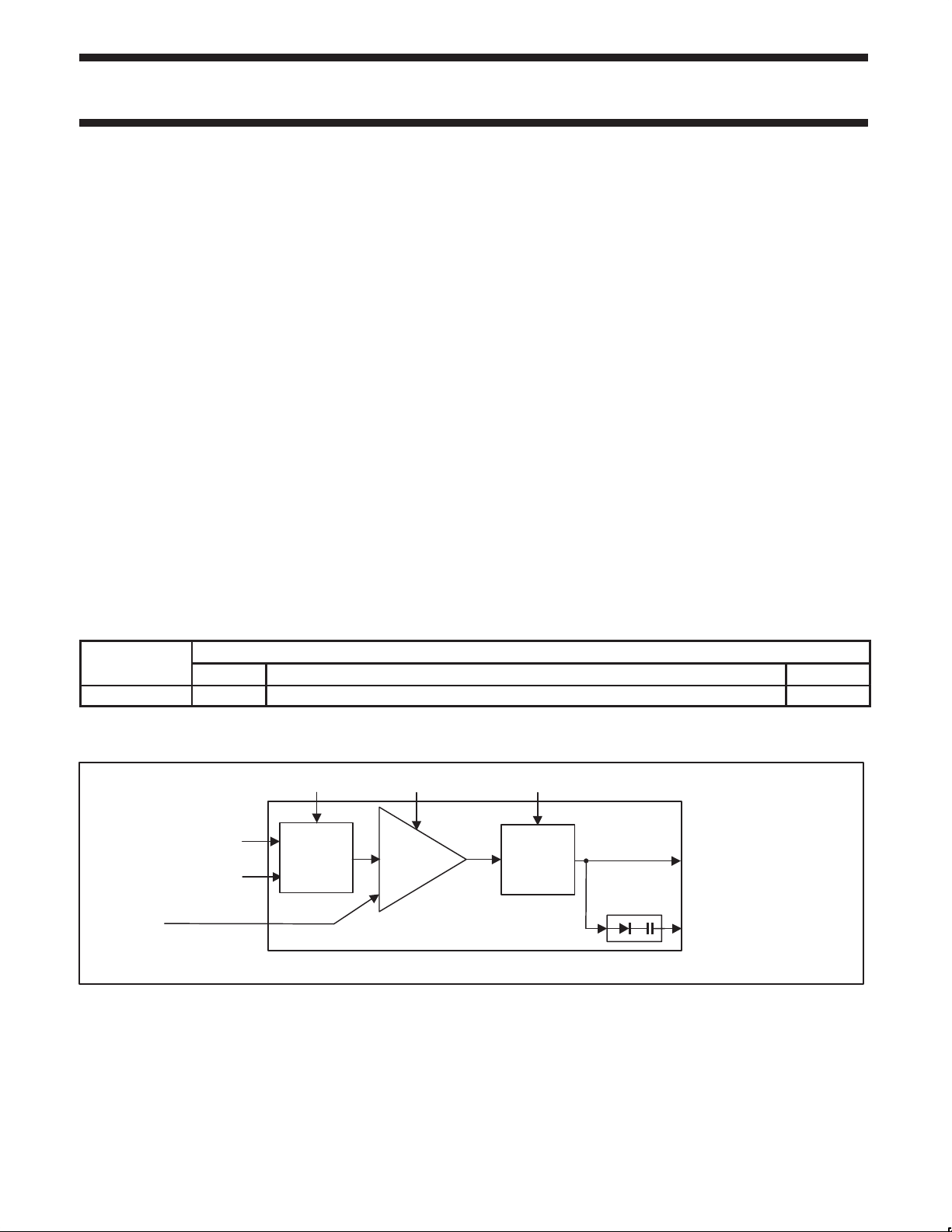
4. BLOCK DIAGRAM
VDD_DRIVER VDD_BIAS VDD_MAIN
IN+
IN–
Power-up power mode
INPUT
MATCH
PA
SA2411
Figure 1. Block diagram
OUTPUT
MATCH
ANT
DETECTOR
SR02383
2003 Feb 07
2
Page 3

Philips Semiconductors Product data
SA2411+20 dBm single chip linear amplifier for WLAN
5. PINNING INFORMATION
16VDD_MAIN
15
14
13
12
11
10
V
_BIAS
DD
PWRUP
GND
RF_GND
ANT
GND
MODE
GND
_DRIVER
V
DD
DETECTOR
1
2
GND
3
IN+
4
IN–
5
GND
6
7
GND
89
SA2411DH
SR02384
Figure 2. Pin configuration
Table 2. Pin description
PIN type is designated by A = Analog, D = Digital, I = Input, O = Output
SYMBOL
VDD_MAIN 1 Analog supply, VDD for power amplifier, 150 mA A
VDD_DRIVER 2 Analog supply, VDD for biasing driver, 35 mA A
GND 3 Grounding A
IN+ 4 Input pin, positive part of balanced signal AI
IN– 5 Input pin, negative part of balanced signal AI
GND 6 Grounding A
DETECTOR 7 Power detector output AO
GND 8 Grounding A
GND 9 Grounding A
MODE 10 Mode switch; floating = high gain, grounded = low gain AI
GND 11 Grounding A
ANT 12 Output pin, RF, to antenna AO
RF_GND 13 RF ground must be connected A
GND 14 Grounding A
PWRUP 15 Power up pin. HIGH = amplifier is on. LOW = amplifier is off. DI
VDD_BIAS 16 Analog supply, VDD for biasing the amplifier, 5 mA A
All GND pins should be connected to ground to guarantee the best performance.
PIN DESCRIPTION TYPE
2003 Feb 07
3
Page 4

Philips Semiconductors Product data
SA2411+20 dBm single chip linear amplifier for WLAN
6. FUNCTIONAL DESCRIPTION
The main building-blocks are:
•Fixed gain amplifier (PA)
•Output matching
•Input matching
•Power Detector
•Power Mode
Input
The device has differential inputs so a balun is needed in the case of single ended operation, input impedance is approximately 75 Ω + 25j Ω,
balanced. The inputs can be DC biased with the pin V
transceiver chip.
Amplifier
The amplifier is a fixed gain, class AB amplifier. There is an additional pin, VDD_BIAS, to adjust the class A bias current. Reducing the class A
currents reduces the gain. This allows trade-offs to be made among gain, linearity and current.
Output matching
The output of the amplifier is matched, on chip, for a 50 Ω load. The matching includes the supply feed for the power amplifier. The pin
V
_MAIN is the main supply for the amplifier. No additional filtering is needed to meet the 802.11b spec.
DD
Power detector
The power detector detects the power level and transforms it into a low frequency current. The detector output must be loaded with a resistor to
ground for the highest accuracy. This resistor has an optimal value of 5.6 kΩ. Lower values can be used to comply with maximum input
sensitivity of ADCs, at the cost of dynamic range. The maximum voltage detected is 2.3 V .
_DRIVER. The input matching is optimized to interface with the SA2400A WLAN
DD
Power mode
This pin selects the desired gain and linearity level (13 dB or 14.5 dB gain). The low gain is more applicable to high voltage applications from
3.3 V to 3.6 V . The high gain is more applicable to low voltage applications lower than 3.3 V.
NOTE:
In order to assure optimal thermal performance, it is recommended that all ground pins be connected, and that the number of vias to ground
under the chip be maximized. In addition, the use of solder mask under the chip (for scratch protection) is not recommended.
2003 Feb 07
4
Page 5
Philips Semiconductors Product data
SA2411+20 dBm single chip linear amplifier for WLAN
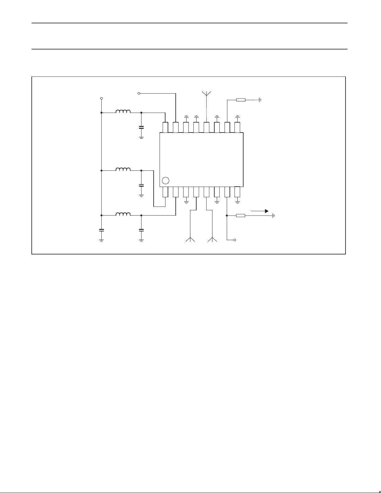
7. CONNECTIVITY DIAGRAM
V
DD
PWRUP
L1
GND
GND
PwrUp
C1
VDD
SA2411
L2
C2
L3
C4 C3
VDD
VDD
GND
RFin
IN+
C1, C2, C3 = 5.6 pF
C4 = 10 nF
R1 = optional connect to ground via 0 W resistor.
R2 = optional resistor to ground to convert current into voltage
L1, L2, L3 = Optional inductors
1 nH … 10 nH, or microstrip lines with length 1 … 10 mm.
No inductors and directly connecting all supplies to V
might cause problems. The optimal values of the inductors
DD
depends on the application board.
ANT
ANT
IN–
RFin
GND
GND
MODE
DET
R1
GND
GND
R2
V
Idet.
det
SR02385
2003 Feb 07
5
Page 6

Philips Semiconductors Product data
SA2411+20 dBm single chip linear amplifier for WLAN
8. OPERATION
The SA2411 linear amplifier is intended for operation in the 2.4 GHz band, specifically for IEEE 802.11 1 and 2 Mbits/s DSSS, and 5.5 and 11
Msymbols/s CCK standards. Throughout this document, the operating RF frequency refers to the ISM band between 2.4 and 2.5 GHz.
Amplifier Output Power
The SA2411 linear amplifier is designed to give at least 19 dBm output power for an 11 Msymbols/s CCK modulated input carrier. At 19 dBm
output power the ACPR specs are met. The fixed gain amplifier amplifies the input signal by 14.5 dB typically.
Power Mode
The biasing can be adjusted to change the gain and therefore the maximum linear output power. For high supply voltages (>3.2 V) the low-gain
mode is advised. For low supply voltages (<3.3 V) the high-gain mode is advised.
Power Mode Pin 9 = Typical output power Typical small
signal Gain
High Floating 20.0 dBm 14.5 dB 35 mA 185 mA @ 20 dBm
Low Grounded 20.0 dBm 13 dB 28 mA 185 mA @ 20 dBm
Typical DC current
(no RF signal)
Typical Current
consumption
Power detector
The power detector current output is linear proportional with the RF output voltage. The RF output power is quadratic proportional to the RF
output voltage. Therefore, the detector is quadratic proportional to the output power. The following relation can be expressed:
P
+k
out
P
is output power in mWatt, V
out
The quadratic factor is 1.5. The sensitivity is then 49 mWatt/V2.
P
out
20 dBm = 100 mW 1.7 V 300 uA
19 dBm = 79 mW 1.4 V 250 uA
17 dBm = 50 mW 1.0 V 175 uA
15 dBm = 32 mW 0.7 V 125 uA
9 dBm = 8 mW 0.3 V 50 uA
The loading of the detector can be different in the application. The highest accuracy is achieved with 5.6 kΩ. But other values can be used to
adapt to the maximum input sensitivity of other circuits. Other detector loading values result in other k-factors. The maximum detector voltage is
limited to about 2.4 V .
Vndetector
is detector voltage in Volt, k = sensitivity in mWatt/V2, n = quadratic factor.
detector
V
(5.6 kΩ load) I
detector
detector
(5.6 kΩ in series)
DC feed at input
There is a possibility to add a DC voltage at the input pins (pin 4 and pin 5) by feeding pin 2. This option should be used in case the SA2411 is
lined up with the SA2400A.
2003 Feb 07
6
Page 7

Philips Semiconductors Product data
SA2411+20 dBm single chip linear amplifier for WLAN
9. OPERATING CONDITIONS
The SA2411 shall meet all of the operating conditions outlined in this section. Table 3 specifies the absolute maximum ratings for the device.
Table 4 gives the recommended operating conditions.
Table 3. Absolute maximum ratings
Symbol Parameter Min Max Unit
T
stg
V
DDa
– Voltage applied to inputs –0.5 VDD+0.5 V
– Short circuit duration, to GND or V
Table 4. Recommended operating conditions
Symbol Parameter Min Nom Max Units
T
amb
V
DDa
Storage temperature –55 +150 °C
Supply voltage (analog) –0.5 +3.85 V
DD
Ambient operating temperature –40 – +85 °C
Supply voltage (analog) 2.85 3.3 3.6 V
– 1 sec
10. SA2411 TRANSMITTER REQUIREMENTS Table 5. SA2411 transmitter specifications
T
= 25 °C; VCC = 3 V; frequency = 2.45 GHz, R
amb
Specification Condition, Remarks Min Nom Max Units
DC
DC current Standard mode (pin 10 is floating) – 35 – mA
DC current Low output power mode (pin 10 is grounded) – 28 – mA
Leakage current Vpwrup = 0 V. Vss = 3.0 V – – 10 µA
AC : 802.11b MODULATION
Output back off (relative to 1 dB compression of single carrier) – 2 – dB
RF frequency 2.4 2.45 2.5 GHz
Input impedance Dif ferential (75 Ω + 25j Ω) – 100 – Ω
Load impedance Single ended – 50 – Ω
Power gain for small signal Mode = High gain, Input level = –20 dBm – 14.5 – dB
Power gain for small signal Mode = Low gain, Input level = –20 dBm – 13 – dB
Output power Meeting the FCC specs of 30 dBc and 50 dBc, mode = high – +20.0 – dBm
Current consumption “ – 200 – mA
Gain “ – 12.5 – dB
Output power Meeting the FCC specs of 30 dBc and 50 dBc, mode = low – +20.0 – dBm
Current consumption “ – 200 – mA
Gain “ – 12.5 – dB
= 5.6 kΩ, unless otherwise stated.
detector
Power ramping up time 10% to 90% ramp up – 0.5 – µs
Power ramping down (when
enabled)
Error Vector Magnitude 11 Msymbols/s QPSK. Both RF outputs. – 5 – %
Isolation Pin 15 (PWRUP) = 0 V – 15 – dB
Harmonic Suppression at 2 and 3
times fundamental frequency
2003 Feb 07
a) 90% to 10% ramp down
b) 10% to carrier leakage level
fundamental frequency output power = +20 dBm – 40 – dBc
7
– 0.5
0.5
– µs
Page 8

Philips Semiconductors Product data
SA2411+20 dBm single chip linear amplifier for WLAN
Table 6. SA2411 Detector specification
T
= 25 °C, VCC = 3.0 V
amb
Specification Condition, Remarks Min Nom Max Units
GENERAL
Detector sensitivity With 5 kΩ load resistor to ground – 49 – mW/V
Detector accuracy per sample At 16 dBm –40 °C to +80 °C; from 2.7 V to 3.6 V – 0.3 – dB
Absolute accuracy From sample to sample – 0.5 – dB
Detector quadratic factor – 1.5 – –
Detector settling time From 10% to 90% of final value – 500 – ns
Spread from sample to sample 20 dBm output power – 1 – dB
Absolute detector voltage 19 dBm output power – 1.4 – V
Absolute detector voltage error From –30 °C to +80 °C;
– 0.15 – V
from 2.7 V to 3.6 V at 19 dBm output power
Detector power range +10 – +21 dBm
2
11. GRAPHS
The following graphs are only for a typical sample measured on a SA2411 test board under nominal condition applying an 11Mb/s CCK 802.11b
modulation. Corrections for input, output and supply losses have been applied. The dotted lines represent the low gain mode. The solid
lines are for the high gain mode.
The first two graphs are small signal graphs. The gain and the DC currents are plotted versus supply voltage.
50
40
30
small signal current[mA]]
20
10
2.7 2.9 3.1 3.3 3.5
DC current versus Supply Voltage
Supply Voltage[V]
Figure 3. DC current vs. supply voltage
SR02464
18.0
16.0
14.0
Small signal gain[dB]]
12.0
10.0
2.7 2.9 3.1 3.3 3.5
Figure 4. Gain vs. supply voltage
Gain versus Supply Voltage
Supply Voltage[V]
SR02465
2003 Feb 07
8
Page 9

Philips Semiconductors Product data
SA2411+20 dBm single chip linear amplifier for WLAN
The next eight graphs are presenting the power sweep for both gain modes at nominal conditions.
22
20
18
16
Pout[dBm]
14
12
10
–4 –2 0 2 4 6 8
Output Power versus Input Power
Pin[dbm]
Figure 5. Output power vs. input power
16
15
Gain versus Output Power
SR02466
25.0%
20.0%
15.0%
10.0%
Efficiency @ 2.7Volt
5.0%
0.0%
Efficiency versus Output Power
–2 2 6 10 14 18 22
Pout[dbm]
Figure 7. Efficiency vs. output power
Current consumption vs Output Power
200
150
SR02468
14
Gain[dB]
13
12
5101520
Pout[dbm]
SR02467
Figure 6. Gain vs. output power
100
Current consumption [mA]
50
0
–10 –6 –2 2 6 10 14 18 22
Pout[dbm]
SR02469
Figure 8. Current consumption vs. output power
2003 Feb 07
9
Page 10

Philips Semiconductors Product data
SA2411+20 dBm single chip linear amplifier for WLAN
–25
–30
–35
ACPR[dBc]
–40
–45
7 121722
ACPR versus Output Power
Pout[dbm]
SR02470
Figure 9. ACPR vs. output power
–46
–50
ALT versus Output Power
Detector Voltage versus Output Power
2
1.5
1
Detector[V]
0.5
0
8 1012 1416 182022
Pout[dbm]
SR02472
Figure 11. Detector voltage vs. output power
1.0
0.5
Detector Error versus Output Power
–54
ALT[dBc]
–58
–62
7121722
Pout[dbm]
SR02471
Figure 10. ALT vs. output power
0.0
Detector error[dB]
–0.5
–1.0
7 121722
Pout[dbm]
SR02473
Figure 12. Detector error vs. output power
2003 Feb 07
10
Page 11

Philips Semiconductors Product data
SA2411+20 dBm single chip linear amplifier for WLAN
The next curves present the frequency dependency for an input power of +7 dBm:
21
20
19
Output Power[dBm]
18
17
2.40E+00 2.43E+00 2.45E+00 2.48E+00 2.50E+00
Output Power versus Frequency
Frequency[GHz]
SR02474
Figure 13. Output power vs. frequency
15
14
Gain versus Frequency
20.0%
15.0%
10.0%
Eficiency[%]
5.0%
0.0%
2.40E+00 2.43E+00 2.45E+00 2.48E+00 2.50E+00
Efficiency versus Frequency
Frequency[GHz]
Figure 15. Efficiency vs. frequency
–28
–30
ACPR versus frequency
SR02476
13
Gain[dB]
12
11
2.40E+00 2.43E+00 2.45E+00 2.48E+00 2.50E+00
Frequency[GHz]
SR02475
Figure 14. Gain vs. frequency
–32
ACPR[dBc]
–34
–36
2.40E+00 2.43E+00 2.45E+00 2.48E+00 2.50E+00
Frequency[GHz]
SR02477
Figure 16. ACPR vs. frequency
2003 Feb 07
11
Page 12

Philips Semiconductors Product data
SA2411+20 dBm single chip linear amplifier for WLAN
–48
–50
–52
ALT[dBc]
–54
–56
2.40E+00 2.43E+00 2.45E+00 2.48E+00 2.50E+00
ALT versus Frequency
Frequency[GHz]
SR02478
Figure 17. ALT vs. frequency
2
1.5
Detector Voltage versus Frequency
1.0
0.5
0.0
Detector Error[dB]
–0.5
–1.0
2.40E+00 2.43E+00 2.45E+00 2.48E+00 2.50E+00
Detector Errror versus Frequency
Frequency[GHz]
SR02480
Figure 19. Detector error vs. frequency
1
Detector voltage[V]
0.5
0
2.40E+00 2.43E+00 2.45E+00 2.48E+00 2.50E+00
Frequency[GHz]
SR02479
Figure 18. Detector voltage vs. frequency
2003 Feb 07
12
Page 13

Philips Semiconductors Product data
SA2411+20 dBm single chip linear amplifier for WLAN
The last 5 curves are characterization data for supply voltage, temperature and power. The worst-case scenario is the combination of highest
temperature/lowest supply. The best-case scenario is the combination of lowest temperature and highest supply voltage. The data has been
taken using a non-modulated carrier at 2.5 GHz.
50.00
45.00
40.00
35.00
DC current [mA]
30.00
25.00
2.8 3.0 3.2 3.4 3.6
Supply Voltage [V]
SR02481
Figure 20. DC current vs. supply voltage, mode = high
17.00
16.00
15.00
Gain [dB]
14.00
13.00
2.8 3.0 3.2 3.4 3.6
Supply Voltage [V]
SR02482
Figure 21. Gain vs. supply voltage, mode = high
–30
0
25
70
85
–30
0
25
70
85
30.00
28.00
26.00
24.00
Efficiency [%]
22.00
20.00
2.8 3.0 3.2 3.4 3.6
Supply Voltage [V]
–30
0
25
70
85
SR02484
Figure 23. Efficiency vs. supply voltage, mode = high
0.50
0.25
0.00
–0.25
Detector Error [dB]
–0.50
2.8 3.0 3.2 3.4 3.6
Supply Voltage [V]
–30
0
25
70
85
SR02485
Figure 24. Detector error vs. supply voltage, mode = high
20.00
19.00
Pout [dBm]
18.00
17.00
2.8 3.0 3.2 3.4 3.6
Supply Voltage [V]
SR02483
Figure 22. Output power vs. supply voltage, mode = high
–30
0
25
70
85
2003 Feb 07
13
Page 14

Philips Semiconductors Product data
SA2411+20 dBm single chip linear amplifier for WLAN
12. APPLICATION WITH THE SA2400A
Next diagram is the application of the SA2400A with the SA2411.
The interface is simple. Two equal microstrip lines connect the SA2400A with the SA2411. The length of this connection should be kept to a
minimum.
The supply for the open collectors of the SA2400A is provided via pin 2 of the SA2411.
C2 is for supply voltage decoupling.
V
PWRUP
DD
PWRUP
GND
RF_GND
ANT
GND
MODE
VDD_BIAS
16 15 14 13 12 11 10 9
GND
RF connection
Other connection
SA2411
12345678
IN–
IN+
GND
VDD_MAIN
VDD_DRIVER
C2
GND
DETECTOR
GND
I
detector
3-WIRE BUS
TX_HI
DD
A_V
TX_OUT_LO
A_GND
SA2400A
TX_OUT_HI_P
AGCRESET
AGCSET
IDCOUT
A_GND
A_GND
48 47 46 45 44 43 42 41 40 39 38 37
1
2
3
4
Figure 25.
NOTE: A suggested starting point for designing the coupled microstrip lines:
Length = 1/18 λ. Width = 12 mils, Separation = 5 mils with the Dielectric constant = 4.6.
This should result in Z
There should be no ground plane under the microstrip lines.
2003 Feb 07
= 150 Ω, Zo = 75 Ω, and Z
even
= 30 Ω.
odd
14
TX_OUT_HI_M
A_GND
SEN
SDATA
SCLK
TX/RX
TX_IN_I_P/
TX_DATA_I
36
TX_IN_I_M/
TX_DATA_Q
35
TX_IN_Q_P
34
TX_IN_Q_M
33
SR02487
Page 15

Philips Semiconductors Product data
SA2411+20 dBm single chip linear amplifier for WLAN
TSSOP16: plastic thin shrink small outline package; 16 leads; body width 4.4 mm SOT403-1
2003 Feb 07
15
Page 16

Philips Semiconductors Product data
SA2411+20 dBm single chip linear amplifier for WLAN
REVISION HISTORY
Rev Date Description
_3 20030207 Product data (9397 750 10825); ECN 853-2346 29486 of 07 February 2003;
_2 20020731 Preliminary data (9397 750 10166).
_1 20020723 Preliminary data (9397 750 10144).
supersedes Preliminary data SA241 1 revision 2 of 31 July 2002 (9397 750 10166).
Modifications:
•Features (Section 2.)
– First bullet: from “75 Ω” to “75 Ω + 25j Ω ”
– delete bullet “1 dB attenuator”
•Block diagram: signal “Power mode” changed to “Power-up power mode”.
•Pin names modified.
•Functional description (Section 6.), Power mode: from “(14 dB or 14.5 dB gain)” to “(13 dB or 14.5 dB gain)”.
•Typical small signal Gain (HIGH) changed from 15 dB to 14.5 dB; (LOW) changed from 14 dB to 13 dB.
•Input impedance (nom) changed from 200 Ω to 100 Ω; Condition changed from “differential (100 + 100 Ω)” to
“differential (75 Ω + 25j Ω)”
•Gain (nom) changed from 13.0 dB to 12.5 dB.
•Output power (nom) changed from +20.5 to +20.0.
•Figures 20 through 24 modified.
•Note added below Figure 25.
2003 Feb 07
16
Page 17

Philips Semiconductors Product data
SA2411+20 dBm single chip linear amplifier for WLAN
Data sheet status
Level
I
Data sheet status
Objective data
[1]
Product
[2] [3]
status
Development
Definitions
This data sheet contains data from the objective specification for product development.
Philips Semiconductors reserves the right to change the specification in any manner without notice.
II
III
[1] Please consult the most recently issued data sheet before initiating or completing a design.
[2] The product status of the device(s) described in this data sheet may have changed since this data sheet was published. The latest information is available on the Internet at URL
[3] For data sheets describing multiple type numbers, the highest-level product status determines the data sheet status.
Preliminary data
Product data
http://www.semiconductors.philips.com.
Qualification
Production
This data sheet contains data from the preliminary specification. Supplementary data will be published
at a later date. Philips Semiconductors reserves the right to change the specification without notice, in
order to improve the design and supply the best possible product.
This data sheet contains data from the product specification. Philips Semiconductors reserves the
right to make changes at any time in order to improve the design, manufacturing and supply. Relevant
changes will be communicated via a Customer Product/Process Change Notification (CPCN).
Definitions
Short-form specification — The data in a short-form specification is extracted from a full data sheet with the same type number and title. For detailed information see
the relevant data sheet or data handbook.
Limiting values definition — Limiting values given are in accordance with the Absolute Maximum Rating System (IEC 60134). Stress above one or more of the limiting
values may cause permanent damage to the device. These are stress ratings only and operation of the device at these or at any other conditions above those given
in the Characteristics sections of the specification is not implied. Exposure to limiting values for extended periods may affect device reliability.
Application information — Applications that are described herein for any of these products are for illustrative purposes only. Philips Semiconductors make no
representation or warranty that such applications will be suitable for the specified use without further testing or modification.
Disclaimers
Life support — These products are not designed for use in life support appliances, devices, or systems where malfunction of these products can reasonably be
expected to result in personal injury . Philips Semiconductors customers using or selling these products for use in such applications do so at their own risk and agree
to fully indemnify Philips Semiconductors for any damages resulting from such application.
Right to make changes — Philips Semiconductors reserves the right to make changes in the products—including circuits, standard cells, and/or software—described
or contained herein in order to improve design and/or performance. When the product is in full production (status ‘Production’), relevant changes will be communicated
via a Customer Product/Process Change Notification (CPCN). Philips Semiconductors assumes no responsibility or liability for the use of any of these products, conveys
no license or title under any patent, copyright, or mask work right to these products, and makes no representations or warranties that these products are free from patent,
copyright, or mask work right infringement, unless otherwise specified.
Contact information
For additional information please visit
http://www.semiconductors.philips.com . Fax: +31 40 27 24825
For sales offices addresses send e-mail to:
sales.addresses@www.semiconductors.philips.com.
Document order number: 9397 750 10825
Koninklijke Philips Electronics N.V. 2003
All rights reserved. Printed in U.S.A.
Date of release: 02-03
2003 Feb 07
17
 Loading...