

Philips sa1638 DATASHEETS

INTEGRATED CIRCUITS
SA1638
Low voltage IF I/Q transceiver
Product specification 1997 Sept 03
IC17 Data Handbook
Philips Semiconductors Product specification
SA1638Low voltage IF I/Q transceiver
DESCRIPTION
The SA1638 is a combined Rx and Tx IF I/Q circuit. The receive
path contains an IF amplifier, a pair of quadrature down-mixers, and
a pair of baseband filters and amplifiers. A second pair of mixers in
the transmit path transposes a quadrature baseband input up to the
IF frequency. An external VCO signal is divided down internally and
buffered to provide quadrature local oscillator signals for the mixers.
A further divider chain, reference divider and phase detector are
provided to avoid the need for an external IF synthesizer. Rx or Tx
path or the entire circuit may be powered down by logic inputs.
On-board voltage regulators are provided to allow direct connection
to a battery supply.
FEATURES
•Direct supply: 3.3V to 7.5V
•Two DC regulators giving 3.0V output
•Low current consumption: 18mA for Rx or 22mA for Tx
•Input/output IF frequency from 70-400 MHz
•Internal IF PLL for synthesizing the local oscillator signal
PIN CONFIGURATION
GNDREG1
VccTxRx
GND1
VREG1
1
VREG2
PON
V
BATT
AOUT
BOUT
DCRES
RESD
RESA
RESB
2
3
4
5
6
7
8
9
10
11
12
13 14 15 16 17 18 19
VREGF2
GNDREG2
•High performance on-board integrated receive filters with
•Switchable alternative bandwidth setting available to allow
•Designed for a widely used I and Q baseband GSM interface
•Control registers power up in a default state
•Optional DC offset trim capability to <200mV
•Only a standard reference input frequency required, choice of 13,
•Fully compatible with SA1620 GSM RF front-end (see Figure 9)
APPLICATIONS
•IF circuitry for GSM 900MHz hand-held units
•IF circuitry for PCN (DCS1800) hand-held units
•Quadrature up and down mixer stage
LQFP Package
RxIF IN
RxIF INX
45464748
GND2
424344
48–pin LQFP
bandwidth tunable between 50-850 kHz
channel bandwidth flexibility in operation
26, 39 or 52MHz
TxIFOUT
TxIFOUTX
GND3
PONPLL
VccCP
394041 3738
20 21 22 23 24
CP
36
35
34
33
32
31
30
29
28
27
26
25
VEECP
I
REF
LO INX
LO IN
ADJ IN
CLK IN
CLK INX
LOCK
STROBE
CLOCK
DATA
V
DIG
EE
V
PONRx
REF
QRxOUT
QRxOUTX
IRxOUT
IRxOUTX
QTx IN
QTx INX
ITx IN
PDTx
ITx INX
VccDIG
SR00524
Figure 1. SA1638 Pin Configuration
ORDERING INFORMATION
DESCRIPTION TEMPERATURE RANGE ORDER CODE DWG #
48-Pin Thin Quad Flat Pack (LQFP)
1997 Sept 03 853-1818 18351
2
-40 to +85°C
SA1638BE SOT313-2

Philips Semiconductors Product specification
SA1638Low voltage IF I/Q transceiver
BLOCK DIAGRAM
PONRx
V
REF
PDTx
TxIFOUT
TxIFOUTX
VCCTxRx
GND3
GND1
RxIF IN
RxIF INX
GND2
LO IN
LO INX
ADJ IN
LOCK
I
REF
PONPLL
V
CC
V
EE
CP
CP
CP
RESA
IF
AMP
RESB
BIAS RX
BIAS TX
CHARGE
PUMP
VREG1
RESD
2
÷
BUFFERS
DETECTOR
÷
GNDREG1
V.REG.1 V.REG.2
N
÷
PHASE
13, 26
39, 52
BATT
V
DC
ADJUST
DC
REGISTER
TEST
REGISTER
SYNTH
REGISTER
PON
VREGF2
GNDREG2
STATUS
REGISTER
SERIAL
INPUT
VREG2
ITx IN
ITx INX
QTx IN
QTx INX
IRxOUT
IRxOUTX
QRxOUT
QRxOUTX
DCRES
AOUT
BOUT
1997 Sept 03
V
DIG
CC
V
DIG
EE
CLK IN
CLK INX
Figure 2. SA1638 Block Diagram
3
DATA
CLOCK
STROBE
SR00525
Philips Semiconductors Product specification
SA1638Low voltage IF I/Q transceiver
PIN DESCRIPTIONS
Pin No. Pin Name Description
1 VREG1 Output voltage of regulator 1
2 VREGF2 Feedback of regulator 2
3 VREG2 Output voltage of regulator 2
4 GNDREG2 Ground of regulator 2
5 PON Power-on input for voltage regulators 1 and 2 (active high)
6 V
BATT
7 AOUT Programmable logic output (see Figure 9)
8 BOUT Programmable logic output (see Figure 9)
9 DCRES Reference current setting resistor for DC offset circuit
10 RESD Additional external current defining resistor for filters
11 RESA Principal external current defining resistor for filters
12 RESB Principal external current defining resistor for filters
13 PONRx Power-on input for Rx (active high)
14 V
15 QRxOUT Differential receive baseband output
16 QRxOUTX Differential receive baseband output
17 IRxOUT Differential receive baseband output
18 IRxOUTX Differential receive baseband output
19 QTx IN Differential transmit baseband input
20 QTx INX Differential transmit baseband input
21 ITx IN Differential transmit baseband input
22 ITx INX Differential transmit baseband input
23 PDTx Power-on for transmitter (active low)
24 VCCDIG Digital circuit supply
25 VEEDIG Digital ground
26 DATA Serial bus data input
27 CLOCK Serial bus clock input
28 STROBE Serial bus strobe input
29 LOCK Test control/synthesizer lock indicator
30 CLK INX Differential reference divider input
31 CLK IN Differential reference divider input
32 ADJ IN Used for test only. Do not connect
33 LO IN Differential LO input
34 LO INX Differential LO input
35 I
36 VEECP Charge pump ground
37 CP Charge pump output
38 VCCCP Charge pump circuit supply
39 POnPLL Power-on input for synthesizer circuits (active high)
40 GND3 Ground (internal connection to GND1 and GND2)
41 TxIFOUTX Differential transmit IFoutput (open collector)
42 TxIFOUT Differential transmit IFoutput (open collector)
43 GND2 Ground (internal connection to GND1 and GND3)
44 RxIF INX Differential receive IF input
45 RxIF IN Differential receive IF input
46 GND1 Ground (internal connection to GND2 and GND3)
47 VCCTxRx Transmit and receive circuits supply voltage (also feedback of Regulator 1)
48 GNDREG1 Ground of regulator 1
NOTE: There are no ESD protection diodes at Pins 41 and 42. Thus, open collector outputs may have increased DC voltage or higher AC
peak voltage.
REF
REF
Input voltage for regulators 1 and 2
Reference voltage
Reference current setting for charge pump
1997 Sept 03
4
Philips Semiconductors Product specification
SYMBOL
PARAMETER
TEST CONDITIONS
UNITS
SA1638Low voltage IF I/Q transceiver
ABSOLUTE MAXIMUM RATINGS
SYMBOL PARAMETER RATING UNITS
VCCXXX Supply voltages: VCCTxRx, VCCDIG, VCCCP -0.3 to +6.0 V
V
BATT
V
IN
∆VG Any GND pin to any other GND pin 0 V
P
D
T
JMAX
P
MAX
T
STG
NOTE:
1. Maximum dissipation is determined by the operating ambient temperature and the thermal resistance, θ
RECOMMENDED OPERATING CONDITIONS
SYMBOL PARAMETER RATING UNITS
VCCXXX Supply voltages: VCCTxRx, VCCDIG 2.7 to 5.5 V
VCCCP Charge pump supply voltage 2.9 to 5.5 V
V
BATT
T
A
Battery voltage -0.3 to +8.0 V
Voltage applied to any other pin -0.3 to (V
+0.3) V
CCXXX
Power dissipation, TA = 25°C (still air) 300 mW
Maximum operating junction temperature 150 °C
Maximum power input/output +20 dBm
Storage temperature range –65 to +150 °C
. 48-pin LQFP: θJA = 67°C/W.
JA
Battery voltage 3.3 to 7.5 V
Operating ambient temperature range -40 to +85 °C
Voltage Regulators
TA = 25°C, PON = 3V, PONRX = 0V, PDTX = 3V, PONPLL = 0V, V
connected to V
V
1,
REG
V
2
REG
V
BATT
I
1, I
OUT
OUT
I
BATT
I
BATT PD
2
C
1
REG
2
C
2
REG
F2; VCCDIG = VCCCP = 3V; unless otherwise stated.
REG
Nominal V
Maximum output current for each
2
regulator
OUT
1
Supply current for both regulators I
Power-down supply current PON = 0V, I
V
1 cap load 0.1 1000 µF
REG
V
2 cap load 0.1 500 µF
REG
LINEREG Line regulation DC, V
LOADREG Load regulation I
BW Bandwidth 100 kHz
F
F
PON
REG
t
ON
Feedthrough attenuation from PON to
each regulator
Feedthrough attenuation from V
each regulator
BATT
to
Turn ON time 10 µs
NOTES:
1. At T
≥ 150°C a thermal switch reduces the output current to avoid damage.
j
2. Recommended load capacitors: In every case C
optional ≤1000µF with series resistance ≤5Ω. The low series resistance is very important to ensure regulator stability.
REG
1 = C
3. Standard deviations are based on the characterization results of 90 ICs.
BATT
= 3.3V, I
OUT
1 = I
2 = 15mA, V
OUT
1 connected to VCCTxRx, V
REG
LIMITS
Min –3σ Typ +3σ Max
2.85 2.93 3.00 3.07 3.15 V
3.3 7.5 V
= 0mA 4.3 5 5.7 7 mA
LOAD
= 0mA 7.7 9 10.3 15 µA
LOAD
= 3.3V to 7.5V –0.4 –0.2 0.001 0.2 0.4 %
BATT
= 15mA to 30mA –5 –0.37 -0.17 0.03 5 %
LOAD
≤ -40 dB
f ≤ 100kHz
f = 10MHz
f = 100MHz
f = 400MHz
2 = 100nF to ground with series resistance ≤0.1Ω. Additional capacitor
REG
≤ -61
≤ -32
≤ -37
≤ -48
REG
30 mA
dB
2
1997 Sept 03
5

Philips Semiconductors Product specification
SYMBOL
PARAMETER
TEST CONDITIONS
UNITS
SYMBOL
PARAMETER
TEST CONDITIONS
UNITS
SA1638Low voltage IF I/Q transceiver
DC ELECTRICAL CHARACTERISTICS
VCCTxRx=VCCDIG=VCCCP=PONRx=PONPLL= +3V; VEEDIG = VEECP=GND1=GND2=GND3=PDTx = 0V; TA = 25°C, unless otherwise stated.
LIMITS
MIN –3σ TYP +3σ MAX
Supply current
Rx and IF synthesizer active
I
CC
Tx and IF synthesizer active
Power-down mode
IV
V
I
OUT
Reference voltage Generated internally 1.39 1.57 1.75 V
REF
V
REF
REFISINK
I
SOURCE
DC output current
Digital inputs (PON)
V
V
High level input voltage range 2.0 V
IH
Low level input voltage range 0 0.8 V
IL
Digital inputs (PDTx, PONRx, PONPLL, PON)
V
V
High level input voltage range 2.0 VCCTxRx V
IH
Low level input voltage range 0 0.8 V
IL
Digital inputs (Clock, Data, Strobe)
V
V
High level input voltage range 2.0 VCCDig V
IH
Low level input voltage range 0 0.8 V
IL
Digital outputs (LOCK, AOUT, BOUT)
V
V
Output voltage HIGH IO = -2mA
OH
Output voltage LOW IO = 2mA 0.4 V
OL
PONRx = PONPLL = PDTx = Hi
PONRx = PDTx = Low;
PONPLL = Hi
PONRx = PONPLL = Low;
PDTx = Hi
At pins TxIFOUT and
TxIFOUTX
14.4 16 17.6 20
17.4 19.5 21.6 24
0.068
5
5
1.5 1.86 2.0 2.14 2.7 mA
BATT
VCCDIG–0.4
mA
µA
V
V
AC ELECTRICAL CHARACTERISTICS
VCCTxRx=VCCDIG=VCCCP=PONRx=PONPLL= +3V; VEEDIG = VEECP=GND1=GND2=GND3=PDTx = 0V; LOIN = 100mV
CLK
= 100mV
IN
, 52MHz; serial registers programmed with default values; TA = 25°C unless otherwise stated. Test Circuit Figure 8.
PEAK
LIMITS
MIN –3σ TYP +3σ MAX
IF Transmit Modulator
BW Input modulation bandwidth 200Ω source impedance 0.82 0.94 1.06 MHz
V
COM
V
IN
Common mode range for
baseband inputs
Peak input signal amplitude Centered on V
Third harmonic distortion
1
DC at pins ITxIN, ITxINx,
QTxIN, QTxINx
COM
| ITxIn | = | ITxInX | =
| QTxIn | = | QTxInX |
= 0.75V
PEAK;
fin = 20kHz
1 1.5 2 V
0.75 V
-61 -57 -53 -40 dB
Between pins: ITxIn and
R
C
INTx
INTx
Input resistance
Input capacitance
ITxInX or QTxIn and
QTxInX
At ITxIn, ITxInX,
QTxIn, QTxInX
112 kΩ
Output saturation limit VCCTxRx-0.3 V
| ITxIn | = | ITxInX | =
I
OUT
S
RMS output current
LO suppression
LO
1
SSB Sideband suppression
1
| QTxIn | = | QTxInX |
= 0.75V
PEAK
| ITxIn | = | ITxInX | =
| QTxIn | = | QTxInX |
= 0.75V
PEAK
; fin = 20k
| ITxIn | = | ITxInX | =
| QTxIn | = | QTxInX |
= 0.75V
PEAK
; fin = 20k
0.6 0.73 0.82 0.91 1.08 mA
+30 +43 dB
+35 +50 dB
, 800MHz;
PEAK
10 pF
1997 Sept 03
6
Philips Semiconductors Product specification
SYMBOL
PARAMETER
TEST CONDITIONS
UNITS
dBc/H
SA1638Low voltage IF I/Q transceiver
AC ELECTRICAL CHARACTERISTICS (Continued)
LIMITS
MIN –3σ TYP +3σ MAX
IF Transmit Modulator (continued)
t
t
OFF
Noise density at 600kHz
Noise density at 10MHz
Turn ON time PdTx = LO, transmit signal to 90% 5 µs
ON
Turn OFF time PdTx = HI, transmit signal to 10% 5 µs
|ITxIn| = |ITxInX| = |QTxIn| =
|QTxInX| = 0.75V
PEAK -133 -131 -129
IF Receiver (R = 36kΩ between pins RESA and RESB)
RInRx Differential input impedance fIN = 400MHz 5 || 0.6 kΩ || pF
ROutRx Output impedance 1 kΩ
Output common mode voltage V
f3dB Low pass filter -3dB bandwidth 70 83 90 kHz
Low pass filter attenuation:
200kHz
400kHz
600kHz
6.5MHz
13.0MHz
Differential output PD into GSM
VG Voltage gain
baseband relative to 1200Ω
source EMF
NF Noise figure
8
1200Ω source and external
matching resistor and inductor
Channel matching:
Gain
fIN = 400.005MHz
Phase
2
Differential, DCRES=562kΩ -60 -25 60 mV
I
V
OUT
OUT
Output DC offset
Output drive current at each pin Source (Sink) 10 (700) µA
Minimum differential output swing 2.0 V
Input 1dB compression point:
In band
P
-1dB
200kHz
400kHz
1200Ω source EMF
600kHz
t
t
OFF
ON
Turn ON time
Turn OFF time
3
POnRx = HI, to baseband signal
out
POnRx = LO, to no baseband
signal out
IF Synthesizer
Local oscillator input frequency
LO
range
9
Differential input impedance
LO peak input voltage range
Between pins LOIN and LOINX, f
= 800MHz
Single-ended
Referred to 50Ω
IN
Z
V
f
LOIN
LOIN
Programmable divider:
Division range
Step size
f
CLKIN
Z
CLKIN
V
CLKIN
I
REF
Reference clock input frequency V
CLKIN
= 100mV
PEAK
Differential input impedance Between pins ClkIn and ClkInX 10 || 1.0 kΩ || pF
CLKIN peak input voltage range Single-ended, referred to 50Ω 50 400 mV
Charge pump input reference
current
Charge pump output current:
| I
|
CP
c0...c2 = 000
c0...c2 = 111
I
=31.2µA,
REF
VCP = VCCCP/2
Step size
0.425
0.045
-130 -129 -128
V
dB
6.5308.9
38.1
REF
10.7
45
70
12.5
51.9
>80
>80
43 49.4 51 52.7 58 dB
5.7 7.0 8.3 dB
-1.5 -0.26
0.0
-59
-54
-55.3
-49.3
-53
-47
-50.7
-44.8
1.5 dB
degrees
-47
-40
dBV
-47
-47
2 µs
2 µs
140 800 MHz
276 || 0.6 Ω || pF
50 100 mV
64
511
1
52 MHz
31.2 µA
0.85
0.487
0.979
0.062
0.5
1.0
0.071
0.513
1.021
0.08
0.575
1.15
0.105
mA
z
1997 Sept 03
7
Philips Semiconductors Product specification
SYMBOL
PARAMETER
TEST CONDITIONS
UNITS
t
ns
SA1638Low voltage IF I/Q transceiver
AC ELECTRICAL CHARACTERISTICS (Continued)
LIMITS
MIN –3σ TYP +3σ MAX
IF Synthesizer (cont.)
DI
CP
I
∆I
CP_M
|I
CP_L
t
t
OFF
Serial Interface
f
CLOCK
t
NOTES:
1. Parameter measured relative to modulation sideband amplitude.
2. After programming the DC offset register for minimum offset. DCRES = 562kΩ.
3. The turn on time relates only to the power up time of the circuit. The settling time of the integrated baseband filters has to be added (for
GSM–mode = 8µs with filter bandwidth setting resistor = 36kΩ).
4. The relative output current variation is defined thus:
5. The output current matching is measured when both (positive current and negative current) sections of the output charge pumps are on.
6. As soon as P
7. Guaranteed by design.
8. NF =
9. Minimium frequency is guaranteed by design.
Relative output current variation
CP
Output current matching
| Output leakage current VCP = 0.3V to VCCCP-0.3V -0.02 0.1 0.22 ±15 nA
Turn ON time
ON
Turn OFF time
7
Clock frequency 10 MHz
Set-up time: DATA to CLOCK,
SU
CLOCK to STROBE
t
Hold time: CLOCK to DATA 30 ns
H
Pulse width: CLOCK 30
W
Pulse width: STROBE 30
ON
ǒ
20log
ƪ
CURRENT
I
2
I
1
I
2
I
1
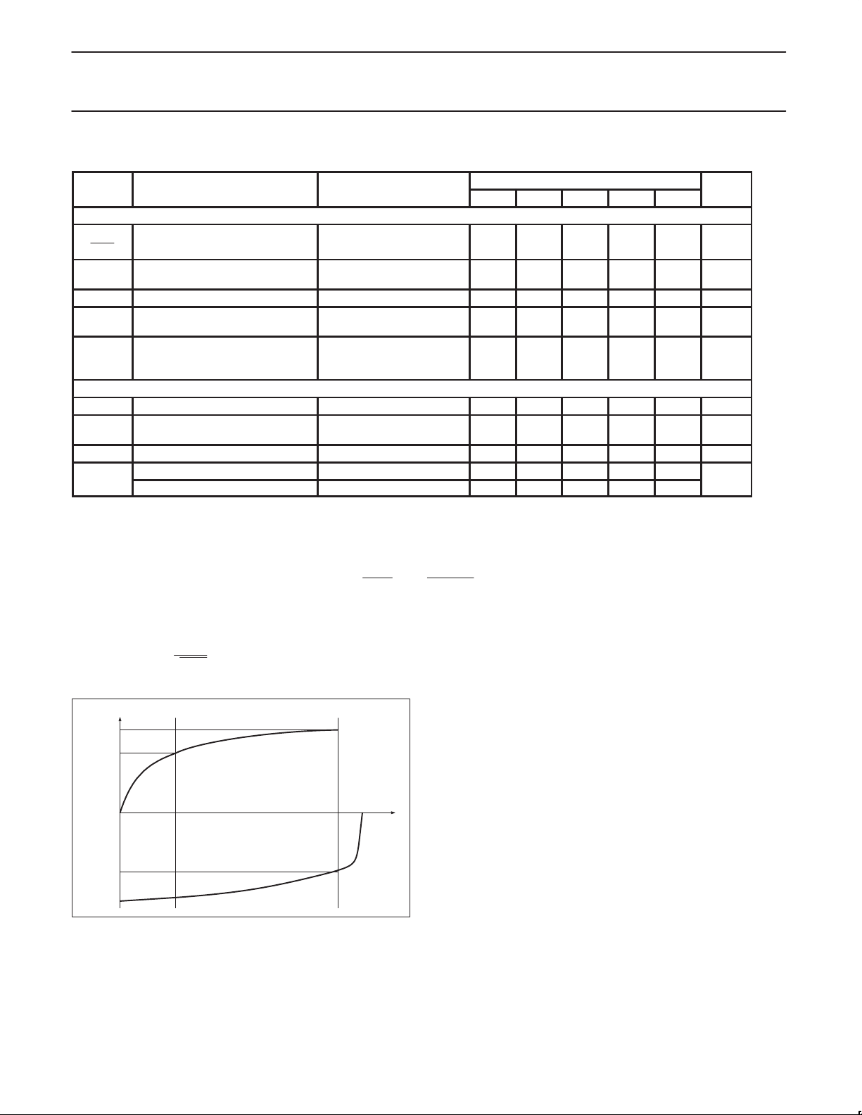
Figure 3. Relative Output Current Variation
6
PLL is set to LO, the phase detector is reset and no charge pumps pulses are generated.
E
no
Ǔ
* VG
ƫ
Ǹ
4kTR
V
1
FUNCTIONAL DESCRIPTION
Serial Programming Input
The serial input is a 3-wire input (CLOCK, STROBE, DATA) to
program the counter ratios, charge pump current, status- and
DC-offset register, mode select and test register. The programming
data is structured into two 21-bit words; each word includes 4 chip
5
where, E
4
I
=31.2µA 0.1 1.3 2.5 ±10 %
REF
I
=31.2µA,
REF
VCP = VCCCP/2
POnPLL = HI, to full charge
pump current
POnPLL = LO, to ICCCP,
ICCDIG <5% of operational
supply current
DI
OUT
I
is the output noise voltage measured in a 1Hz bandwidth, R = 1200Ω, VG = gain in dB.
no
VOLTAGE
V
2
SR00526
+ 2@
±12 %
15 µs
15 µs
30 ns
(I
* I1)
2
|(I
; with V1 = 0.3V, V2 = VCCCP – 0.3V (see Figure 3).
) I1)|
2
address bits and 1 subaddress bit. Figure 2 shows the timing
diagram of the serial input. When the STROBE = L, the clock driver
is enabled and on the positive edges of the CLOCK the signal on
DATA input is clocked into a shift register. When the STROBE = H,
the clock is disabled and the data in the shift register remains stable.
Depending on the value of the subaddress bit the data is latched
into different working registers. Table 3 shows the contents of each
word.
Default States
Upon power up (VCCDIG is applied) a reset signal is generated,
which sets all registers to a default state. The logic level at the
STROBE pin should be low during power up to guarantee a proper
reset. These default states are shown in Table 3.
Reference Divider
The reference divider can be programmed to four different division
ratios (:13, :26, :39, :52), see registers r0, r1; default setting: divide
by 13.
Main Divider
The external VCO signal, applied to the LOIN and LOINX inputs, is
divided by two and then fed to the main divider (:N). The main
divider is a programmable 9 bit divider, the minimum division ratio is
1997 Sept 03
8
 Loading...