

Philips SA1630BE Datasheet

INTEGRATED CIRCUITS
SA1630
IF quadrature transceiver
Product specification 1998 Jul 21
IC17 Data Handbook
Philips Semiconductors Product specification
SA1630IF quadrature transceiver
DESCRIPTION
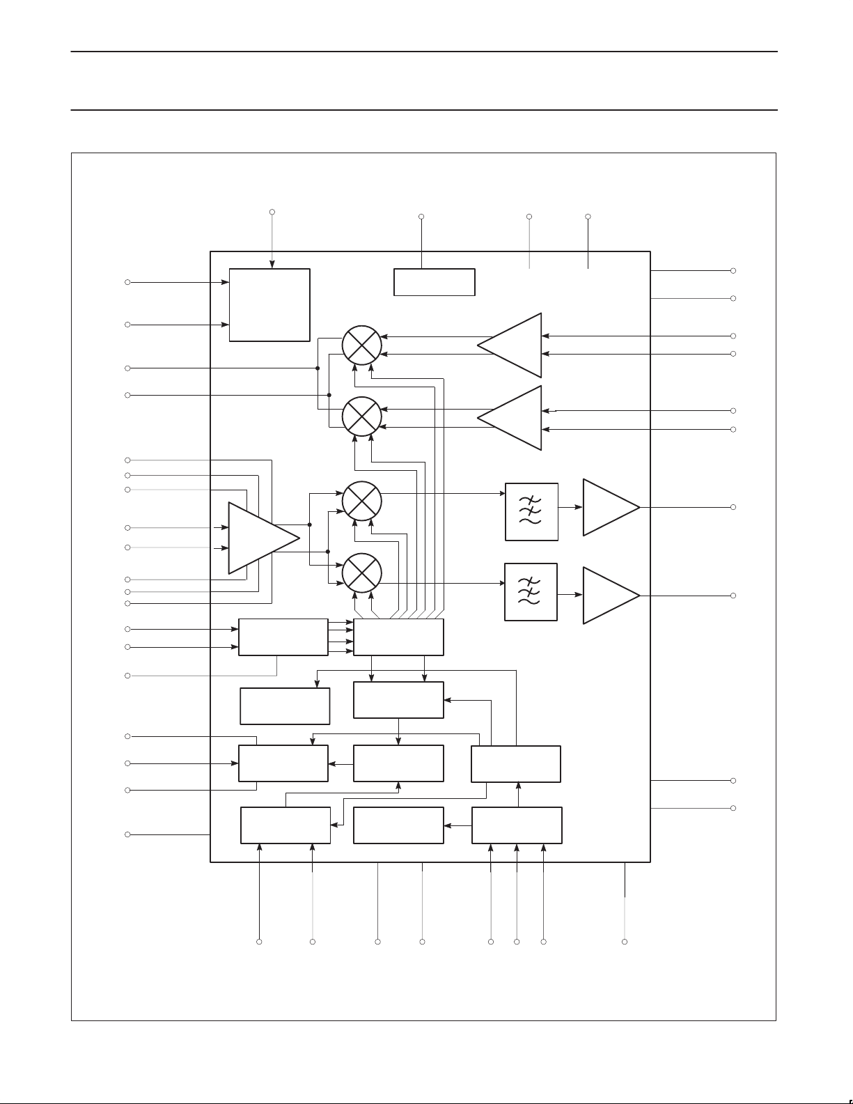
The SA1630 is a 70–400 MHz I/Q transceiver for wireless LAN.
The Receive Path contains a digitally gain controlled linear IF
amplifier, a pair of quadrature down conversion mixers and a pair of
baseband amplifiers. The transmit path contains a pair of quadrature
up conversion mixers that transposes a quadrature baseband input
signal up to IF frequency. An external VCO signal is divided
internally and provides quadrature local oscillator signals for the
mixers. Another divider chain, reference divider and phase detector
are provided to avoid the need for an external synthesizer. To keep
power consumption to a minimum the transmit, receive and local
oscillator functions can be powered down under digital control.
FEA TURES
•Low supply voltage operation of 2.7V for main chip and 2.9V for
charge pump.
•Low current consumption: 33.5 mA in RX, 26.5 mA in TX, typical
at 3V .
•Flexible power up/down options.
•Optional 2.5V regulated reference voltage available during
transmit.
•Input IF frequency range of 70–400 MHz.
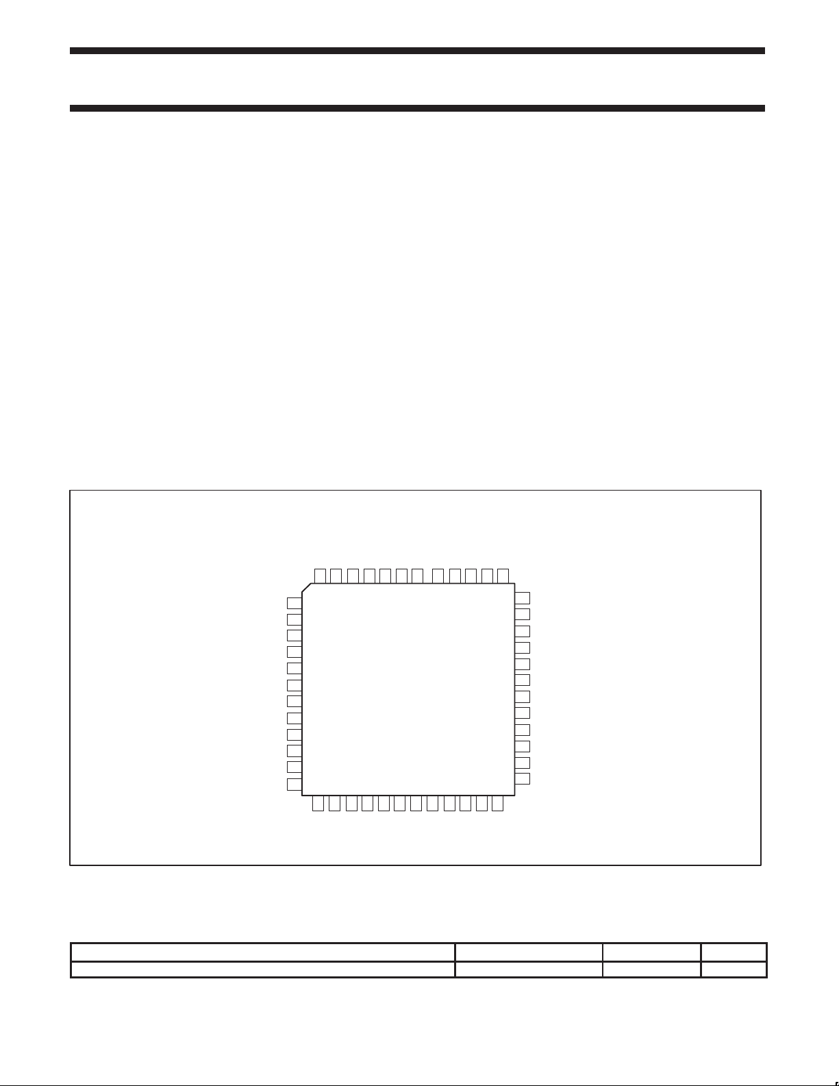
BE Package
IF IN
IF INX
V
CC
GNDRX
V
CC
PLL_ON
Rx_ON
GNDHDR
GC0
GC1
GC2
GC3
GC4
GC5
GNDRx
Rx
1
2
3
Rx
4
5
6
7
8
9
10
11
12
13 14 15 16 17 18 19
GNDRxRxRx
GNDRXTxTx
45464748
•Internal IF PLL for synthesizing the local IF oscillator signal.
•Bandwidth of baseband Tx inputs is 20 MHz and that of baseband
Rx outputs is 8.5MHz.
•Designed for IEEE 802.11 wireless LAN using Direct Sequence
Spread Spectrum modulation.
•Control registers power up in a default state.
•Only a standard reference input frequency required, choice of 8,
11, 22 or 44 MHz.
•Digital gain control of 70 dB in steps of 2 dB.
•Rx Baseband amplifiers are capable of driving 1k ||15pF
•Rx Baseband o/p’s clamp symmetrically , above 1Vp–p in order to
prevent dc bias shift under overdrive conditions.
•Package: LQFP–48, PCMCIA compatible
APPLICATIONS
•IF circuitry for IEEE 802.11 DSSS wireless LAN.
•Applications for high speed wireless data.
IFOUT
IFOUTX
424344
20 21 22 23 24
GNDTxRx
GNDTxRx
CC
V TxRx
394041 3738
REF
REF
V 2.5
I
36
35
34
33
32
31
30
29
28
27
26
25
GNDCP
CP
V CP
CC
DATA
CLOCK
STROBE
LOCK
LO_INX
LO_IN
GNDRx
CLK IN
CLK
INX
GND_BB
GND_BB
CC
V _BB
Q_RxOUT
I_Tx_IN
I_RXOUT
Q_Tx IN
I_Tx_INX
CC
Q_Tx INX
V _DIG
Tx_ON
GNDDIG
SR01549
Figure 1. Pin Configuration
ORDERING INFORMATION
DESCRIPTION TEMPERATURE RANGE ORDER CODE DWG #
48–Pin Plastic Low Profile Quad Flat package –40 to +85°C SA1630BE SOT313–2
1998 Jul 21 853–2049 19763
2
Philips Semiconductors Product specification
SA1630IF quadrature transceiver
(46)
(45)
(10)
(11)
(12)
(4)
PLL–ON
R
Tx
Tx
IFOUT
Tx
IFOUTX
LO IN
LO INX
XON
MODE
ON
CONTROL
÷
2
(5)
(23)
(43)
(42)
(7)
GC0
(8)
GC1
(9)
GC2
Rx
IFIN
Rx
IFINX
GC3
GC4
GC5
(28)
(29)
(38)
2.5V REGULATOR
BUFFERS
V
2.5
REF
(1,3)
VCCR
(39)
VCCTXR
X
X
GND_BB
VCC_BB
I_Tx
IN
I_Tx
INX
Q_Tx
IN
Q_Tx
INX
I_Rx
Q_Rx
OUT
OUT
1
1
(13, 14)
(15)
(18)
(19)
(20)
(21)
(17)
(16)
(34)
(35)
(37)
(30)
(36)
V
CCCP
CP
I
REF
LOCK
GNDCP
CHARGE
8, 11, 22, 44
÷
CLK
IN
DAC
PUMP
N
÷
PHASE
DETECTOR
TEST REGISTER
INX
V
CCDIG
GND DIGCLK
Figure 2. Block Diagram
SYNTH
REGISTER
SERIAL
INPUT
DATA CLOCK STROBE
(2, 27, 44, 47, 48)(31)(32)(33)(24)(22)(25)(26)
GND RX
GND HDR
GNDTXR
(6)
X
(40, 41)
SR01551
1998 Jul 21
3

Philips Semiconductors Product specification
SA1630IF quadrature transceiver
PIN DESCRIPTIONS
Pin No. Pin Name Description
1, 3 VCCRx Supply Pin for Rx section (IF circuits)
2, 27,
44,47,
13, 14 GND_BB Ground pin for Rx baseband circuits
40,41 GNDTxRx Ground pins used by Tx circuits
GNDRx Ground pins for Rx section (IF circuits)
48
4 PLL_ON One of the three digital CMOS logic control inputs to the mode control section
5 Rx_ON One of the three digital CMOS logic control inputs to the mode control section
6 GNDHDR Substrate ground
7 GCO Control bit 0 for IF VGA gain control, CMOS input
8 GC1 Control bit 1 for IF VGA gain control, CMOS input
9 GC2 Control bit 2 for IF VGA gain control, CMOS input
10 GC3 Control bit 3 for IF VGA gain control, CMOS input
11 GC4 Control bit 4 for IF VGA gain control, CMOS input
12 GC5 Control bit 5 for IF VGA gain control, CMOS input
15 VCC_BB Supply Pin for Rx Baseband circuits
16 Q_RXOUT Quadrature–phase Rx baseband output, single–ended
17 I_RxOUT In–phase Rx baseband output, single–ended
18 I_Tx IN In–phase differential Tx baseband input, positive
19 I_Tx INX In–phase dif ferential Tx baseband input, negative
20 Q_Tx IN Quadrature differential Tx baseband input, positive
21 Q_Tx INX Quadrature differential Tx baseband input, negative
22 VCC_DIG Supply for digital circuits
23 Tx_ON One of the Three digital CMOS logic control inputs to the mode control section
24 GNDDIG Digital ground
25 CLK INX Dif ferential reference input for synthesizer, negative
26 CLK IN Differential reference input for synthesizer, positive
28 LO_IN Differential LO input,positive
29 LO INX Differential LO input, negative
30 LOCK Test control output and synthesizer lock indicator
31 STROBE Serial bus strobe input
32 CLOCK Serial bus clock input
33 DATA Serial bus data input
34 VCCCP Supply for charge pump circuits
35 CP Charge pump output
36 GNDCP Ground for charge pump circuits
37 I
REF
38 V
39 VCCTxRx Supply pin used by Tx circuits
42 TxIFOUTX Differential transmitter IF output (open collector), positive
43 TxIFOUT Differential transmitter IF output (open collector), negative
45 RxIF INX Differential receiver IF input, negative
46 RxIF IN Differential receiver IF input, positive
2.5 Reference voltage of 2.5V available for external use
REF
Charge pump reference current
1998 Jul 21
4
Philips Semiconductors Product specification
SA1630IF quadrature transceiver
ABSOLUTE MAXIMUM RATINGS
SYMBOL PARAMETER RATING UNITS
V
CCXX
V
IN
∆VG Any GND pin to any other GND pin 0 V
P
D
T
JMAX
P
MAX
T
STG
RECOMMENDED OPERATING CONDITIONS
SYMBOL PARAMETER RATING UNITS
V
CCXXXX
VCCCP Charge pump supply voltage 2.7 to 3.6 V
T
A
NOTES:
1. There are no ESD protection diodes between pins 42, 43 and V
reduced. Proper ESD handling precautions should be followed.
MODE CONTROL
NO: PLL_ON RX_ON TX_ON STATE DESCRIPTION MODE 2.5V REF
1 0 X X SLEEP mode SLEEP Off
2 1 0 1 Synthesizer ON, Rx STDBY, Tx OFF WAIT Off
3 1 1 1 Synthesizer ON, Rx STDBY, Tx ON TRANSMIT On
4 1 1 0 Synthesizer ON, Rx ON, Tx OFF RECEIVE Off
5 1 0 0 Synthesizer ON, Rx OFF, Tx ON TRANSMIT Off
’0’ – LOGIC LOW
’1’ – LOGIC HIGH
’X’ – DON’T CARE
Supply voltages -0.3 to +6.0 V
Voltage applied to any other pin -0.3 to V
Power dissipation, TA = 25°C (still air) 300 mW
Maximum operating junction temperature 150 °C
Maximum power input/output +20 dBm
Storage temperature range –65 to +150 °C
Supply voltages: 2.7 to 3.6 V
Operating ambient temperature range -40 to +85 °C
to allow higher AC peak voltage. The ESD protection level has thus been
CC
+0.3 V
CCXX
1. Sleep mode (PLL OFF, Rx OFF, Tx OFF)
In this mode everything is switched off except the 3–wire digital bus.
As long as the digital supply is still on, the programmed values are
active and the 3–wire bus will continue to be programmable.
2. Wait Mode (Tx Off, Rx Standby)
PLL is on. Receiver is in the reduced current standby mode and the
transmitter is completely switched off. This mode maybe useful if the
PLL is to be kept on and is waiting for a quick turn–on to either
transmit or receive modes, especially when Rx outputs are AC
coupled.
3. Transmit mode (Rx standby)
The PLL and transmitter are on. The receive section is in a reduced
current mode wherein most of the Rx circuitry is powered down
except for the bias and baseband circuits needed to hold the
baseband output voltages in the active state. This mode is useful if
the Rx baseband outputs are AC coupled via a large capacitor and
the application demands quick turn–on for the Rx, from Tx.
4. Receive Mode (Tx Off)
The Transmitter is completely shut–off. The PLL and receiver
sections are operating.
5. Transmit Mode (Rx OFF)
PLL and Transmit sections are on. However, the Receiver is
completely shut–down. This mode is useful if the Rx baseband
outputs are DC coupled to the external world.
1998 Jul 21
5
Philips Semiconductors Product specification
SA1630IF quadrature transceiver
RX VGA CONTROL TABLE
GC5 GC4 GC3 GC2 GC1 GC0 DECIMAL NUMBER
0 0 0 0 0 0 0 0
0 0 0 0 0 1 1 –2
0 0 0 0 1 0 2 –4
0 0 0 0 1 1 3 –6
0 0 0 1 0 0 4 –8
0 0 0 1 0 1 5 –10
0 0 0 1 1 0 6 –12
0 0 0 1 1 1 7 –14
0 0 1 0 0 0 8 –16
0 0 1 0 0 1 9 –18
0 0 1 0 1 0 10 –20
0 0 1 0 1 1 11 –22
0 0 1 1 0 0 12 –24
0 0 1 1 0 1 13 –26
0 0 1 1 1 0 14 –28
0 0 1 1 1 1 15 –30
0 1 0 1 1 1 23 –32
0 1 1 0 0 0 24 –34
0 1 1 0 0 1 25 –36
0 1 1 0 1 0 26 –38
0 1 1 0 1 1 27 –40
0 1 1 1 0 0 28 –42
0 1 1 1 0 1 29 –44
0 1 1 1 1 0 30 –46
0 1 1 1 1 1 31 –48
1 1 0 1 0 0 52 –50
1 1 0 1 0 1 53 –52
1 1 0 1 1 0 54 –54
1 1 0 1 1 1 55 –56
1 1 1 0 0 0 56 –58
1 1 1 0 0 1 57 –60
1 1 1 0 1 0 58 –62
1 1 1 0 1 1 59 –64
1 1 1 1 0 0 60 –66
1 1 1 1 0 1 61 –68
1 1 1 1 1 0 62 –70
REDUCTION
FROM Gmax
1998 Jul 21
6
Philips Semiconductors Product specification
SYMBOL
PARAMETER
TEST CONDITION
UNITS
SA1630IF quadrature transceiver
DC ELECTRICAL CHARACTERISTICS
VCCXXX=+3V; VEEXXX = 0V; TA=25°C, unless otherwise stated.
LIMITS
MIN TYP MAX
I
CC–4
I
CC–2
I
CC–3
I
CC–1
I
CC–5
V
REF
Z
OUT_VREF
Supply Current, Receive (mode #4)
Supply Current, Wait (mode #2)
Supply Current, Transmit (mode #3)
Supply Current, Sleep mode (mode #1)
Supply current transmit (mode 5)
_2.5 Reference voltage (mode 3, enabled) Load = 1.5mA 2.5 V
Output impedance of reference voltage ∆I = 1.4 to 1.6mA 15
CMOS LOGIC INPUTS (DATA, CLOCK, STROBE)
V
IH
V
I
C
Input logic 1 level 2.0 V
Input logic 0 level 0 0.8 V
IL
Input logic current 1 µA
I
Input logic capacitance 4 pF
I
CMOS Logic output (LOCK)
V
OH
V
OL
Output logic 1 level IO = –2mA V
Output logic 0 level IO = 2mA 0.4 V
CMOS Logic Inputs (PLL_ON, RX_ON, TX_ON)
V
IH
V
I
Input logic 1 level
Input logic 0 level 0 0.8 V
IL
Input logic current 1 µA
I
PLL_ON=Rx_ON=Hi
Tx_ON = Low
Wait mode (2)
PLL_ON = Hi
Tx_ON = Hi
Rx_ON = Low
PLL_ON = TX_ON = Hi
RX_ON = Hi
PLL_ON = Low
RX_ON = DC
TX_ON = DC
PLL_ON = Hi
TX_ON = RX_ON = Low
33.5 41.5 mA
17 23 mA
26.5 34.5 mA
0.012 0.1 mA
22 28.5 mA
CCD
–0.4 V
CCD
2.0
V
CCTXRX
V
V
1998 Jul 21
7
 Loading...