

Philips sa1620 DATASHEETS

INTEGRATED CIRCUITS
SA1620
Low voltage GSM front-end transceiver
Product specification
Supersedes data of 1996 Oct 08
IC17 Data Handbook
1997 May 22

Philips Semiconductors Product specification
SA1620Low voltage GSM front-end transceiver
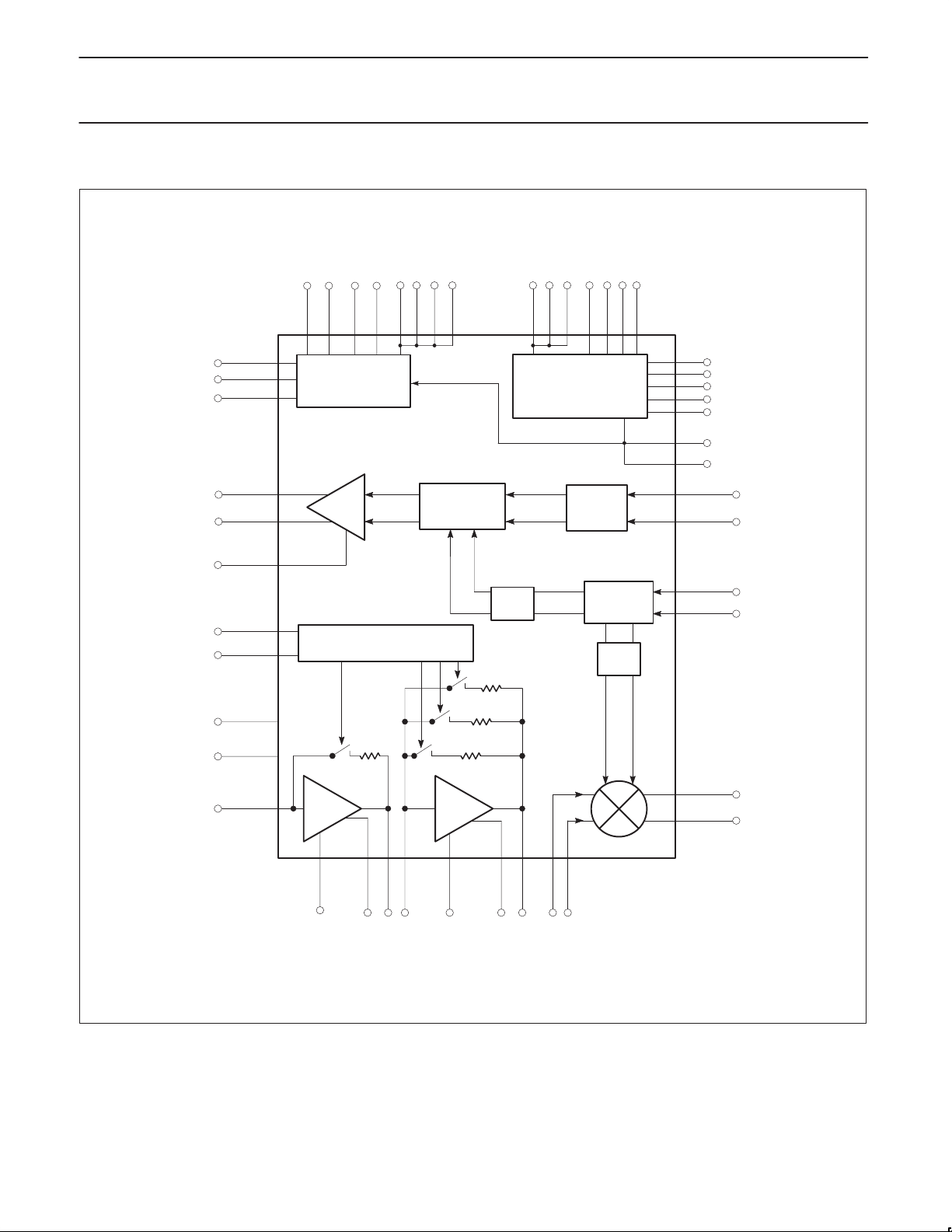
DESCRIPTION
The SA1620 is a combined receive (Rx) and transmit (Tx) front-end
for GSM cellular telephones. The receive path contains two low
noise amplifiers (LNA1 and LNA2) with four switchable attenuation
steps. A Gilbert Cell mixer in the receive path down-converts the
RF signal to a first IF of 70 to 500 MHz. A second Gilbert Cell in the
transmit path transposes a GMSK or phase modulated IF to RF by
image reject mixing and has a fixed IF of 400 MHz. A buffered LO
signal is fed to Rx and Tx mixers. Rx or Tx path or the entire circuit
may be powered-down.
FEA TURES
•Excellent noise figure: <2dB for the LNAs at 950MHz
•LNAs matched to 50Ω with external matching components
•LNAs with gain control, 59dB dynamic range in four discrete steps
•LNA gain stability ±0.5dB within -40 to 85°C
PIN CONFIGURATION
LQFP Package
VccL1
OUT1
GNDL1A
GNDL1
45464748
1
V
CCL2
2
IN2
3
GNDL2
OUT2
INM
INMX
COMP2
COMP1
BM
CC
4
5
6
B
7
A
8
9
10
11
12
13 14 15 16 17 18 19
GNDL2A
V
•Feedthrough attenuation LNA1 to Rx mixer ≥ 35dB
•Tx power adjustable from -3 to +12dBm by external resistor
•Direct supply: 2.7V to 5.5V
•Battery supply voltage V
= 3.3V to 7.5V or direct supply
BATT
•Two DC regulators programmable for 3.0V, 3.4V, 3.7V or 5.1V
•Low current consumption: 28mA for Rx or 59mA for Tx
•Fully compatible with SA1638 GSM IF Digital I/Q circuit
APPLICATIONS
•900MHz front end for GSM hand-held units
•Portable radio, TDMA systems
IN1
RETx
GNDTx3
TxO
Tx0X
GNDTx4
PDTx
424344
48–PIN LQFP
394041 3738
20 21 22 23 24
PONBUF
36
35
34
33
32
31
30
29
28
27
26
25
V
BATT
PON
GNDREG1
VREG1
VREGF2
VREG2
GNDREG2
CON1
LO INX
LO IN
CON2
GNDTx2
PONRx
GNDBM
GND1
RxIF
RxIFX
GND2
TxIF
TxIFX
GND3
VccTx1
GNDTx1
VccTx2
SR00127
Figure 1. Pin Configuration
ORDERING INFORMATION
DESCRIPTION TEMPERATURE RANGE ORDER CODE DWG #
48-Pin Thin Quad Flat Pack (TQFP)
-40 to +85°C
SA1620BE SOT313-2
RECOMMENDED OPERATING CONDITIONS
SYMBOL PARAMETER RATING UNITS
V
CCXX
V
BATT
T
A
1997 May 22 853-1784 18066
Supply voltages 2.7 to 5.5 V
Battery voltage 3.3 to 7.5 V
Operating ambient temperature range -40 to +85 °C
2
Philips Semiconductors Product specification
SA1620Low voltage GSM front-end transceiver
BLOCK DIAGRAM
BM
COMP1
COMP2
VCCGNDBM
GNDTx2
GNDTx1
GNDTx3
GNDTx4
GND1
GND2
GND3
PON
BATT
V
CON1
CON2
PDTx
PONRx
PONBUF
TxOX
RETx
VCCL1
VCCL2
TxO
IN1
TxIF
TxIFX
LO IN
LO INX
RxIF
RxIFX
VREG2
VREG2F2
GNDREG2
GNDREG1
VREG1
VCCTx1
VCCTx2
BANDGAP
BIAS SUPPLIES
SINGLE
SIDEBAND
MIXER
A
B
LNA1
ATTENUATION
CONTROL LOGIC
LNA2
VOLTAGE REGULATORS
TLO
BUFFER
TLOX
LINEAR
IF LEVEL
CONTROL
LO INPUT
BUFFER
BUFFER
RLO
RLOX
1997 May 22
GNDL1
OUT1
IN2
GNDL1A
GNDL2
Figure 2. Block Diagram
INM
OUT2
GNDL2A
INMX
SR00129
3
Philips Semiconductors Product specification
SA1620Low voltage GSM front-end transceiver
PIN DESCRIPTIONS
Pin No. Pin Name Description
DC Regulators
15 GND1 Ground of regulator supply
18 GND2 Ground of regulator supply
21 GND3 Ground of regulator supply
26 CON2 Control 2, voltage select for regulator 1
29 CON1 Control 1, voltage select for regulator 1
30 GNDREG2 Ground of regulator 2
31 VREG2 Output of regulator 2
32 VREG2F2 Feedback of regulator 2
33 VREG1 Output of regulator 1
34 GNDREG1 Ground of regulator 1
35 PON Power-on input of regulators
36 V
Rx Path
10 COMP2 Capacitor for bias stabilization
11 COMP1 Capacitor for bias stabilization
12 VCCBM VCC for Rx Bias and Rx mixer
NOTES:
1. Device is ESD sensitive. There are no ESD protection diodes at Pins 16, 17, 40 and 41. Thus, open-collector outputs may have increased
DC voltage or higher AC peak voltage.
2. Pins 15, 18 and 21 are connected to each other and to a separate ground in REG1 and REG2.
3. Pins 23, 25, 42 and 39 are connected to each other and to the Tx path, LO buffer and associated bias supplies.
4. Pins 22 and 24 are connected to each other providing a sense input. They are also connected to the Tx path, LO buffer and associated bias
supplies.
5. Pins 30 and 34 are not internally connected. They must be connected to external grounds.
6. Pins 48, 1, and 12 are not internally connected and have no ESD protection diodes between them. Power may be saved by connecting
V
BATT
1 VCCL2 Positive supply for LNA2
2 IN2 Input LNA2
3 GNDL2 Ground L2 for LNA2
4 GNDL2A Ground L2A for LNA2
5 OUT2 Output LNA2
6 B Attenuation select B for LNA1 and LNA2
7 A Attenuation select A for LNA1 and LNA2
8 INM RF input for Rx mixer, open emitter
9 INMX Inverse RF input for Rx mixer, open
L1 and IN1 or VCCL2 and IN2 to ground if LNA1 or LNA2 is not needed.
CC
and 2
and 2
Input of regulator 1 and 2
emitter
Pin No. Pin Name Description
13 GNDBM Ground for Rx Bias and Rx mixer
14 PONRx Power on input for Rx bias supply
16 RxIF IF output, open collector
17 RxIFX Inverse IF output, open collector
44 IN1 Input to LNA1
45 GNDL1 Ground L1 for LNA1
46 GNDL1A Ground L1A for LNA1
47 OUT1 Output LNA1
48 VCCL1 Positive supply for LNA1
Tx Path
19 TxIF IF input for Tx
20 TxIFX Inverse IF input for Tx
22 VCCTx1 Positive supply for Tx input
23 GNDTx1 Ground for Tx input
24 VCCTx2 Positive supply for LO and Tx input
25 GNDTx2 Ground for LO and Tx input
38 PDTx Power down Tx input
39 GNDTx4 Ground for Tx output
40 TxOX Inverse Tx output, open collector
41 TxO Tx output, open collector
42 GNDTx3 Ground 1 for Tx output side
43 RETx Reference resistor for Tx output current
Elements for Tx and Rx Path
27 LO IN Input for Local Oscillator signal
28 LO INX Inverse input for LO or AC ground
37 PONBUF Power on first stage LO input buffer and
bias
1997 May 22
4

Philips Semiconductors Product specification
SA1620Low voltage GSM front-end transceiver
ABSOLUTE MAXIMUM RATINGS
SYMBOL PARAMETER RATING UNITS
V
CCXX
V
BATT
V
IN
∆V VCCTx1,2 pins to VCCBM -0.3 to +1 V
∆VG Any GND pin to any other GND pin 0 V
P
D
T
JMAX
P
MAX
T
STG
V
, V
TXO
TXOX
V
, V
RXIF
RXIFX
NOTE:
1. Maximum junction temperature is determined by the power dissipation is determined by the operating ambient temperature and the thermal
resistance, θ
Supply voltages -0.3 to +6.0 V
Battery voltage -0.3 to +8.0 V
Voltage applied to any other pin -0.3 to (V
+0.3) V
CCXX
Power dissipation, TA = 25°C (still air) 800 mW
Maximum operating junction temperature 150 °C
Maximum power input/output +20 dBm
Storage temperature range –65 to +150 °C
Positive RF peak voltage at Tx outputs 6 V
Positive IF peak voltage at Rx mixer outputs 6 V
. 48-pin TQFP: θJA = 67°C/W.
JA
DC REGULA TORS
Two low drop regulators (REG1 and REG2) are included on the chip
and may be used to deliver the supply voltage of the main circuitry
(e.g., 3V) out of the battery (at V
Figure 4 and in Table 1.
REG1 is intended to supply, at least, the internal functions of the
SA1620. Both regulators may also be used for external circuitry.
For this application, different voltages may be programmed as
shown in Table 1.
The transmitter supply pins (V
connection in the feedback loop of REG1 and must be externally
connected to pin VREG1. For REG2, the sensor pin VREGF2 must
be connected to VREG2.
All ground pins are internally bonded to the header except for pins
GNDL1, GNDREG1 and GNDREG2.
When both regulators are not used, connect pins V
CON1, CON2, VREG1, VREG2 and VREG2F2 to ground.
= 3.3 to 7.5V) as shown in
BATT
Tx1,2) also operate as a sensor
CC
, PON,
BATT
Table 1. DC Reg Output Voltage Control Pins
CON1 CON2 VREG1 VREG2 UNITS
L L 3 ± 5% 3 ± 5% V
L H 3.4 ± 5% 3.4 ± 5% V
H L 3.7 ± 5% 3.7 ± 5% V
H H 5.1 ± 5% 5.1 ± 10% V
NOTES:
1. Logic levels at CON1 and CON2:
H – Open circuit. Pin must not be connected externally.
Logic high level supplied on chip.
L – Connected to ground.
2. Currents at CON1 and CON2:
H – 0µA
L (PON = H) – 50µA
L (PON = L) – <1µA
1997 May 22
5

Philips Semiconductors Product specification
SYMBOL
PARAMETER
UNITS
6
F
7
f
dB
SA1620Low voltage GSM front-end transceiver
Table 2. DC Regulators
and V
LIMITS
VREG1
VREG2
REG2
/10 mA
/10 mA
at V
BATT
= 3.3V,
kHz
TEST
V
BATT
VREG1,
VREG2
I
INT1
I
INT2
I
, I
INT01
I
VREG1MAX
I
VREG2MAX
BW
CONDITIONS
Common positive input voltage at both regulators VREG1+0.3 V
Output voltages of regulators 1 and 2 V
= 3.3V 2.85 3 3.15 V
BATT
Internal current of REG1 in power-on mode 4 + I
Internal current of REG2 in power-on mode 2.5 + I
Internal current in power-down mode <15 µA
INT02
5
Max output current at VREG1 100 mA
5
Max output current at VREG2 30 mA
V
V
V
BATT
BATT
BATT
= 3.3V, I
= 3.3V, I
= 7.5V, I
= 0.1mA 0.03
REG1
= 100mA 60
REG1
= 100mA 80
REG1
MIN TYP MAX
≤100kHz ≤–61
10MHz ≤–32
REG
100MHz ≤–37
400MHz ≤–48
NOTES:
1. Power-on pin of Regulator 1 and 2: PON
2. Input currents at PON: <1µA. There are no pull-up or pull-down resistors.
3. Feedthrough attenuation from the logic input PON to the outputs VREG1 and VREG2: ≥40dB.
4. Recommended load capacitors: C529 = C530 = 1µF to ground with series resistance ≤0.1Ω. See Figure 4. Additional optional capacitor
≤1000µF with series resistance ≤5Ω.
≥ 150°C a thermal switch reduces the output current.
5. At T
j
6. Typical open loop bandwidths of regulator 1 at V
7. Feedthrough attenuation (at the indicated frequency f) from the input V
(CON1=CON2=L)
= 3V and C529 = 1µF.
REG1
to the outputs V
BATT
REG1
1997 May 22
6
Philips Semiconductors Product specification
SYMBOL
PARAMETER
TEST CONDITIONS
UNITS
VR1Internal supply at pin RET
V
IR1Current at pin RET
mA
SA1620Low voltage GSM front-end transceiver
DC ELECTRICAL CHARACTERISTICS
V
= +3V, TA = 25°C; unless otherwise stated.
CCxxx
LIMITS
MIN TYP MAX
Transmitter
I
VCC
R1 External resistor
Total supply current
1
pp
p
p
x
x
Low noise amplifiers
I
L1 Current at pin VCCL1 G1hi mode 2.5 3.5 5 mA
VCC
I
L2 Current at pin VCCL2 G2hi mode 2.5 3.5 5 mA
VCC
Receiver
I
VCC
Total supply current
Regulators
Vreg1 Voltage @ 100mA load Con1 Con2
L L 2.85 3.0 3.15 V
L H 3.23 3.4 3.57 V
H L 3.515 3.7 3.885 V
H H 4.61 5.1 5.61 V
Vreg2 Voltage @ 30mA load Con1 Con2
L L 2.85 3.0 3.15 V
L H 3.23 3.4 3.57 V
H L 3.515 3.7 3.885 V
H H 4.61 5.1 5.61 V
Logic levels
V
V
V
I
C
2
Logic 1 level PONBUF, PDTx, PONRx, A, B 2.0 V
IH
Logic 1 level P
IH
Logic 0 level 0 0.8 V
IL
Input logic current 1 µA
I
Input logic capacitance 1.7 pF
Ia
NOTES:
+ I
1. The output current I
2. Thresholds are independent of supply voltages. Thus the SA1620 is compatible with SA1638 and with the power down inputs of usual
TXO
is adjustable by the external resistor R546. I
TXOX
external voltage regulators.
3. P
ON
logic 1 max is V
BATT
.
Transmit mode
= 240Ω
R
546
59 90 mA
240 Ω
VCCTx1,2 = 2.7V 0.43
VCCTx1,2 = 5.5V 0.45
R546 = 240Ω, VCCTx1,2 = 2.7V 1.7
R546 = 240Ω, VCCTx1,2 = 5.5V 1.8
Receive mode
= 240Ω
R
546
ON
+ I
TXO
TXOX
= 10 * I
2.0 V
, I
R546
R546
28 39 mA
= VR1/R546,
CCBM
BATT
3
V
V
1997 May 22
7
Philips Semiconductors Product specification
SYMBOL
PARAMETER
TEST CONDITIONS
UNITS
S
dB
∆S21/∆T
Gain temperature sensitivit
dB/°C
S
dB
∆S21/∆T
Gain temperature sensitivit
dB/°C
SA1620Low voltage GSM front-end transceiver
AC ELECTRICAL CHARACTERISTICS
V
= +3V, TA = 25°C; RF = 940MHZ; IF=400MHz, fLO=RF + IF; LO = –15dBm; unless otherwise stated.
CCXX
1
LIMITS
1
Low Noise Amplifier LNA1
MIN
2
-3σ TYP 3σ MAX
G1hi mode 9.4 10 10.6
Gain
21
G1hi mode, RF = 1800MHz –2.5
G1lo mode –13 –12 –11
IP3 G1lo mode 28
G1hi mode 0.003
G1lo mode 0.0140
∆S21/
∆V
CCL1
p
y
Gain/voltage sensitivity 0.1 dB/V
∆S21/∆f Gain frequency variation 0.01 dB/MHz
S
S
S
P
-1dB
Reverse isolation G1hi mode –19 dB
12
11
22
Input match
Output match
3
3
50Ω –11 dB
50Ω –14 dB
Input 1dB gain compression G1hi mode –15.5 –14 –12.5 dBm
IIP3 Input third order intercept –5.5 –4 –2.5 dBm
IIP3/∆t Input third order intercept 0.011 dB/°C
NF Noise figure 1.9 dB
t
ON
t
OFF
Low Noise Amplifier LNA2
Turn-on time 7 µs
Turn-off time 0.5 µs
2
G2hi mode 9 10 11 dB
G2hi mode, RF = 1800MHz –1.5 dB
Gain
G2lo1 mode –8.5 –7.5 –6.5
G2lo2 mode –22.5 –21.5 –20.5
21
G2lo3 mode –30 –28.5 –27
G2lo1 mode 18
IP3
G2lo2 mode 20
G2lo3 mode 25
G2hi mode 0.003
G2lo1,2,3 modes 0.014
∆S21/
∆V
CCL2
p
y
Gain/voltage sensitivity 0.1 dB/V
∆S21/∆f Gain frequency variation 0.01 dB/MHz
S
S
S
P
-1dB
Reverse isolation G2hi mode –24 dB
12
11
22
Input match
Output match
3
3
50Ω –13 dB
50Ω –15 dB
Input 1dB gain compression G2hi mode –18 –16 –14 dBm
IIP3 Input third order intercept –8 –6 –4 dBm
IIP3/∆t Input third order intercept 0.019 dB/°C
NF Noise figure 2 dB
t
t
ON
OFF
Turn-on time 7 µs
Turn-off time 0.5 µs
1
°
°
1997 May 22
8
 Loading...