

Philips S42SD-YD09, S42AX-YD02, S50HW-YD01, S63HW-XD05 Service Manual
Published by MW 0670 BG CD Customer Service Printed in the Netherlands Subject to modification EN 3122 785 16381
©
Copyright 2006 Philips Consumer Electronics B.V. Eindhoven, The Netherlands.
All rights reserved. No part of this publication may be reproduced, stored in a
retrieval system or transmitted, in any form or by any means, electronic,
mechanical, photocopying, or otherwise without the prior permission of Philips.
Colour Television Module
SDI PDP 2K6
S42SD-YD09 (42-inch SD, v5)
S42AX-YD02 (42-inch HD, w1)
S50HW-YD01 (50-inch HD, w1)
S63HW-XD05 (63-inch HD, v4)
Contents Page
1. Technical Specifications, Connections, and Chassis
Overview 2
2. Safety Instructions, Warnings, and Notes 9
3. Directions For Use 10
4. Mechanical Instructions 11
5. Service Modes, Error Codes, and Fault Finding 21
6. Block Diagrams, Test Point Overview, and
Waveforms 56
7. Circuit Diagrams and PWB Layouts 62
8. Alignments 62
9. Circuit Descriptions, Abbreviation List, and IC Data
Sheets 79
10. Spare Parts List 80
11. Revision List 81
Technical Specifications, Connections, and Chassis Overview
EN 2 SDI PDP 2K61.
1. Technical Specifications, Connections, and Chassis Overview
Index of this chapter:
1.1 PDP Overviews
1.2 Serial Numbers
1.3 Chassis Overviews
Notes:
• Figures can deviate due to the different model executions.
• Specifications are indicative (subject to change).
1.1 PDP Overviews
Table 1-1 PDP overview
Table 1-2 PDP vs Chassis overview
In above table the link is given between the SDI Plasma Display
Panel and the Philips TV chassis (incl. chassis manual no.).
1.1.1 42" SD v5
Figure 1-1 Rear view of plasma panel (42” SD v5)
Figure 1-2 Location of mounting screws (42” SD v5)
NOTE: screw torque 9.5 ± 0.5 kgf.cm
PDP Type / Version Model Name H x V Pixel
1 42” SD v5 S42SD-YD09 852 x 480
2 42” HD w1 S42AX-YD02 1024 x 768
3 50” HD w1 S50HW-YD01 1366 x 768
4 63” HD v4 S63HW-XD05 1366 x 768
Display type Model # Chassis Chassis Manual #
42" SD v5 42PF5521D/10 LC4.41E AB 3122 785 16230
42" SD v5 42PF5521D/12 LC4.41E AB 3122 785 16230
42" HD w1 42PF9431D/37 BJ2.5U PA 3122 785 15930
42" HD w1 42PF9631D/37 BJ2.4U PA 3122 785 15920
50" HD w1 50PF9631D/37 BJ2.4U PA 3122 785 15920
50" HD w1 50PF9731D/37 BJ2.4U PA 3122 785 15920
63" HD v4 63PF9631D/37 BJ3.0U PA 3122 785 16460
No Item Specification 42” SD v5
1 Pixel 852 (H) x 480 (V) pixels
(1 pixel = 1 R,G,B cells)
2 Number of Cells 2556 (H) x 480 (V)
3 Pixel Pitch 1.095 (H) mm x 1.110 (V) mm
4 Cell Pitch R 0.365 (H) mm x 1.110 (V) mm
G 0.365 (H) mm x 1.110 (V) mm
B 0.365 (H) mm x 1.110 (V) mm
5 Display size 932.940 (H) x 532.800 (V) mm
6 Screen size Diagonal 42" Colour Plasma Display Module
7 Screen aspect 16:9
8 Display colour 16.77 million colours (8-bit)
9 Viewing angle Over 160 deg (angle with 50% and greater brightness
perpendicular to PDP module)
10 Dimensions 982 (W) x 582 (H) x 54 (D) mm
11 Weight 1 Module About 15.4 kg
14 Vertical frequency
and
Video/Logic Interface
60 Hz/ 50 Hz, LVDS
G_16380_001.eps
190606
G_16380_002.eps
190606
Technical Specifications, Connections, and Chassis Overview
EN 3SDI PDP 2K6 1.
1.1.2 42" HD w1
Figure 1-3 Rear view of plasma panel (42” HD w1)
Figure 1-4 Location of mounting screws (42” HD w1)
NOTE: screw torque 9.5 ± 0.5 kgf.cm
1.1.3 50" HD w1
Figure 1-5 Rear view of plasma panel (50” HD w1)
Figure 1-6 Location of mounting screws (50” HD w1)
NOTE: screw torque 9.5 ± 0.5 kgf.cm
No Item Specification 42” HD w1
1 Pixel 1.024 (H) x 768 (V) pixels
(1 pixel = 1 R,G,B cells)
2 Number of Cells 3072 (H) x 768 (V)
3 Pixel Pitch 0.912mm (H) x 0.693mm (V)
4 Cell Pitch R Horizontal 0.304 mm
Vertical 0.693 mm
G Horizontal 0.304 mm
Vertical 0.693 mm
B Horizontal 0.30 4 mm
Vertical 0.693 mm
5 Display size 933.89 (H) x 532.22 (V) mm
6 Screen size Diagonal 42" Colour Plasma Display Module
7 Screen aspect 16:9
8 Display colour 1073.7 million colours (10-bit)
9 Viewing angle Over 160 deg (angle with 50% and greater
brightness perpendicular to PDP module)
10 Dimensions 982 (W) x 582 (H) x 54 (D) mm
11 Weight 1 Module About 16.8 kg
12 Vertical frequency
Video/Logic Interface
60/50 Hz, LVDS
G_16380_003.eps
190606
G_16380_004.eps
190606
No Item Specification 50” HD w1
1 Pixel 1366 (H) x 768 (V) pixels
(1 pixel = 1 R,G,B cells)
2 Number of Cells 4,098 (H) x 768 (V) cells
3 Pixel Pitch 0.810 mm (H) x 0.810 mm (V)
4 Cell Pitch R Horizontal 0.270 mm
Vertical 0.810 mm
G Horizontal 0.270 mm
Vertical 0.810 mm
B Horizontal 0.270 mm
Vertical 0.810 mm
5 Display size 1106.46 mm (H) x 622.08 mm (H)
6 Screen size Diagonal 50" Colour Plasma Display Module
7 Screen aspect 16:9
8 Display colour 549.75 billion colours (13-bit)
9 Viewing angle Over 160 deg (angle with 50% and greater
brightness perpendicular to PDP module)
10 Dim ensions 1175 (W) x 678.5 (H) x 63.8 (D) mm
11 We ight Module 1 About 18.0 kg
12 Vertical frequency
Video/Logic Interface
60/50 Hz, LVDS
G_16380_005.eps
190606
G_16380_006.eps
190606

Technical Specifications, Connections, and Chassis Overview
EN 4 SDI PDP 2K61.
1.1.4 63" HD v4
Figure 1-7 Rear view of plasma panel (63” HD v4)
Figure 1-8 Location of mounting screws (63” HD v4)
NOTE: screw torque 9.5 ± 0.5 kgf.cm
1.2 Serial Numbers
Figure 1-9 Location of the serial number
Figure 1-10 Explanation of the serial number
No Item Specification 63” HD v4
1 Pixel 1366 (H) x 768 (V) pixels
(1 pixel = 1 R,G,B cells)
2 Number of Cells 4,098 (H) x 768 (V) cells
3 Pixel Pitch 1.02 mm (H) x 1.0 2 mm (V)
4 Cell Pitch R Horizontal 0.34 mm
Vertical 1.02 mm
G Horizontal 0 .34 mm
Vertical 1.02 mm
B Horizontal 0.34 mm
Vertical 1.02 mm
5 Display size 1393.3 mm (H) x 783.4 mm (H)
6 Screen size Diagonal 63" Colour Plasma Display Module
7 Screen aspect 16:9
8 Display colour 1073.7 million colours (13-bit)
9 Viewing angle Over 160 deg (angle with 50% and greater
brightness perpendicular to PDP module)
10 Dimensions approx. 1680 (W) x 875 (H) x 750 (D) mm
11 Weight Module 3 About 44.0 kg
12 Vertical frequency
Video/Logic Interface
60/50 Hz, LVDS
G_16380_035.eps
121006
G_16380_036.eps
121006
}G
zGuUG
G_16380_007.eps
190606
C 001 A 5 1 03 A 0 0 0 1
Serial No : 0001~9999
Shift : A = Day, B = Afternoon,
C = Night
Day: 01 ~ 31
Month : 1 ~ C
(Oct = A, Nov = B, Dec = C)
Year : 0 (2000) ~ 9 (2009)
Line No : A ~ Z
Type : 272 (50HDW1)
Factory: C [= Cheonan]
S [= Shenzen]
Type : 310 (42HDW1)
Type : 298 (42SDV5)
G_16380_008.eps
161006
Type : 327 (63HDV4)
Technical Specifications, Connections, and Chassis Overview
EN 5SDI PDP 2K6 1.
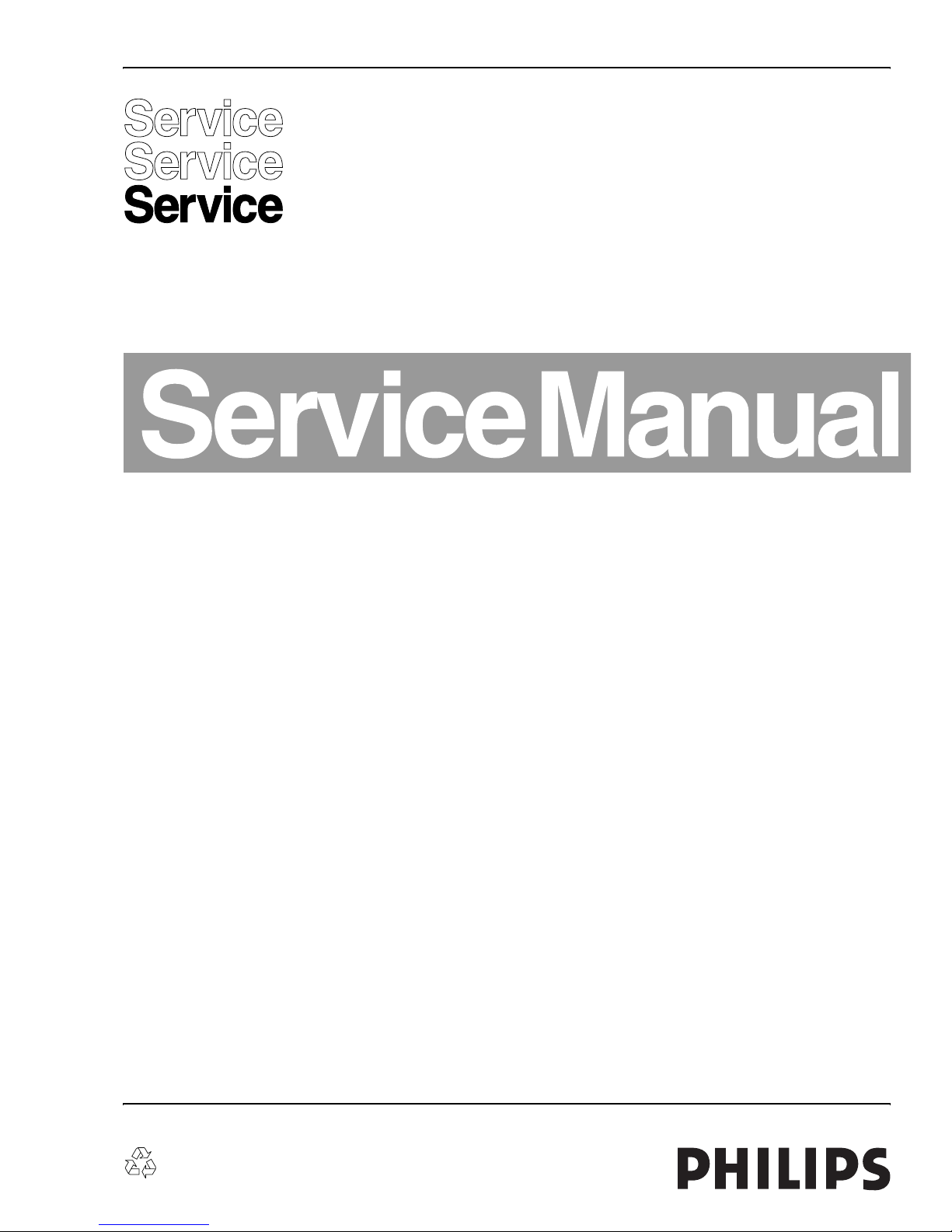
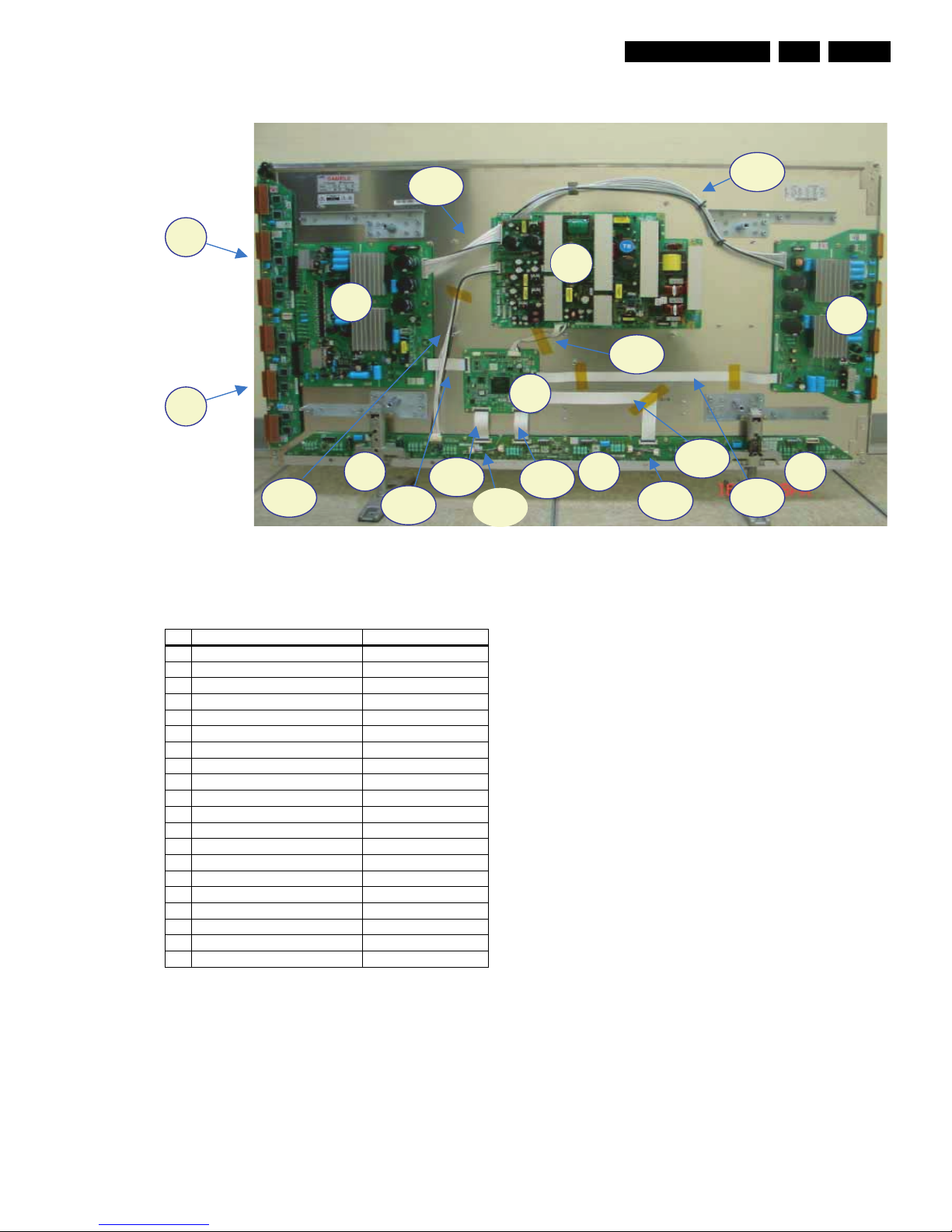
1.3 Chassis Overviews
1.3.1 42” SD v5
Figure 1-11 PWB location (42” SD v5)
Table 1-3 PWB overview (42” SD v5)
X
Y
ZG[G
\G ]
^G
`G_G XW XX
XY
XZG X[
X\G
X]
G_16380_009.eps
190606
No. Location Name
1 SMPS SMPS
2 LOGIC-MAIN Board Assy PWB Logic Main
3 X-MAIN Driving Board Assy PWB X Main
4 Y-MAIN Driving Board Assy PWB Y Main
5 LOGIC E BUFFER Board Assy PWB buffer
6 LOGIC F BUFFER Board Assy PWB buffer
7 Y-BUFFER Board Assy PWB buffer
8 LOGIC + Y-MAIN Lead connector
9 LOGIC + X-MAIN Lead connector
10 LOGIC + LOGIC BUF (E) FFC cable-flat
11 LOGIC + LOGIC BUF (F) FFC cable-flat
12 LOGIC BUF (E) + (F) Lead connector
13 SMPS + LOGIC BUF (E) Lead connector
14 SMPS + LOGIC MAIN Lead connector
15 SMPS + Y-MAIN Lead connector
16 SMPS + X-MAIN Lead connector

Technical Specifications, Connections, and Chassis Overview
EN 6 SDI PDP 2K61.
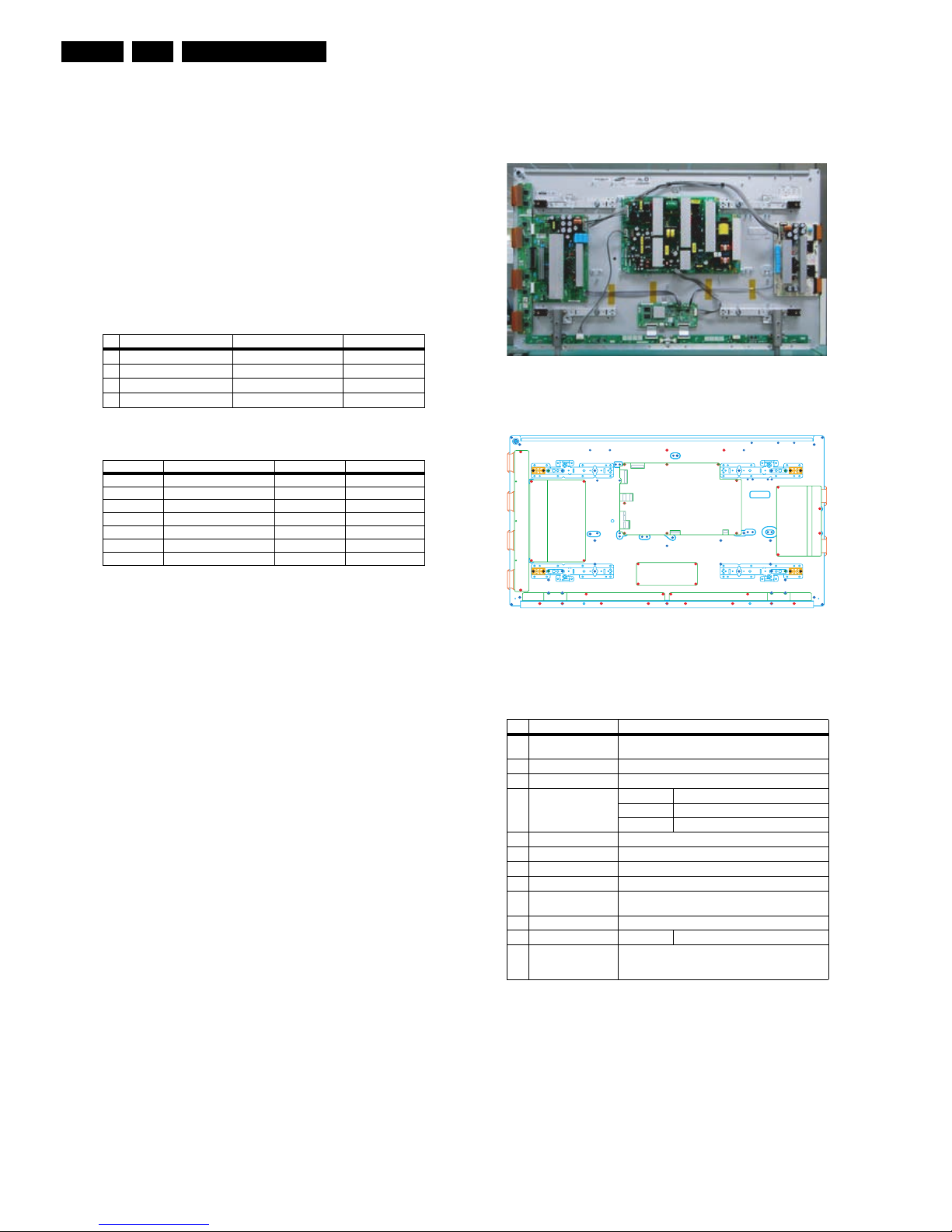
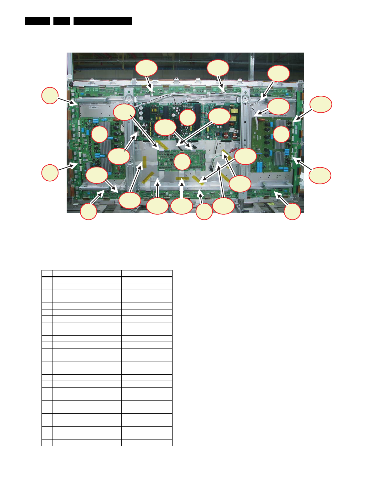
1.3.2 42” HD w1
Figure 1-12 PWB location (42” HD w1)
Table 1-4 PWB overview (42” HD w1)
X
Y
ZG
[G
\G
]
^G
`G
_G
XW
XX
XY
XZ
X[
X\G
X]
G_16380_010.eps
190606
No. Location Name
1 SMPS SMPS
2 LOGIC-MAIN Board Assy PWB LOGIC Main
3 X-MAIN Driving Board Assy PWB X Main
4 Y-MAIN Driving Board Assy PWB Y Main
5 LOGIC E BUFFER Board Assy PWB Buffer
6 LOGIC F BUFFER Board Assy PWB Buffer
7 Y-BUFFER Board Assy PWB Buffer
8 LOGIC + Y-MAIN Lead connector
9 LOGIC + X-MAIN Lead connector
10 LOGIC + LOGIC BUF(E) FFC Cable-flat
11 LOGIC + LOGIC BUF(F) FFC Cable-flat
12 LOGIC BUF(E) + LOG. BUF(F) Lead connector
13 SMPS + LOGIC BUF(E) Lead connector
14 SMPS + LOGIC MAIN Lead connector
15 SMPS + Y-MAIN Lead connector
16 SMPS + X-MAIN Lead connector
Technical Specifications, Connections, and Chassis Overview
EN 7SDI PDP 2K6 1.
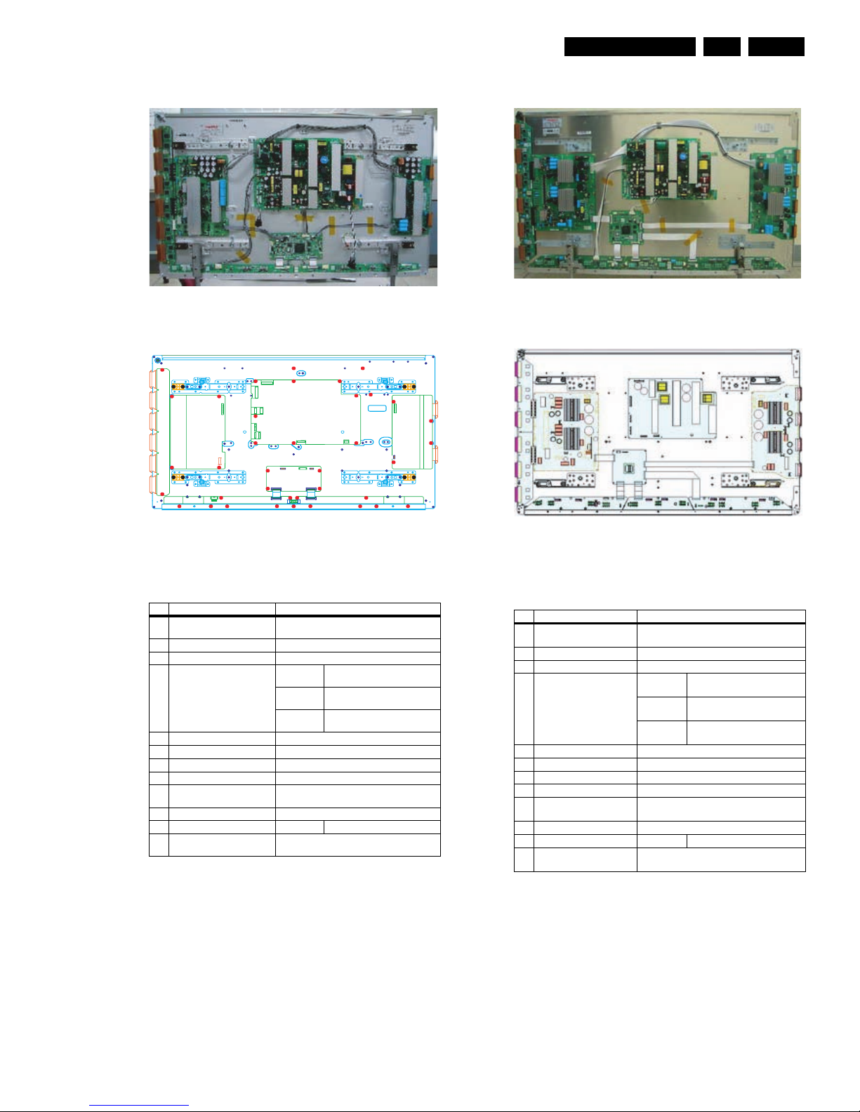
1.3.3 50” HD w1
Figure 1-13 PWB location (50” HD w5)
Table 1-5 PWB overview (50” HD w1)
X
Y
ZG
[G
\G
]
^G
`G
_G
XW
XX
XY
XZ
X[
X\G
X]
X^
X_
X`
YW
G_16380_011.eps
190606
No. Location Name
1 SMPS SMPS
2 LOGIC-MAIN Board Assy PWB LOGIC Main
3 X-MAIN Driving Board Assy PWB X Main
4 Y-MAIN Driving Board Assy PWB Y Main
5 LOGIC E BUFFER Board Assy PWB Buffer E
6 LOGIC F BUFFER Board Assy PWB Buffer F
7 LOGIC G BUFFER Board Assy PWB Buffer G
8 Y-BUFFER (Upper) Board Assy PWB Buffer
9 Y-BUFFER (Lower) Board Assy PWB Buffer
10 LOGIC + Y-MAIN FFC Cable-flat
11 LOGIC + X-MAIN FFC Cable-flat
12 LOGIC + LOGIC BUF (E) FFC Cable-flat
13 LOGIC + LOGIC BUF (F) FFC Cable-flat
14 LOGIC + LOGIC BUF (G) FFC Cable-flat
15 LOGIC BUF (E) + LOG. BUF (F) Lead connector
16 LOGIC BUF (F) + LOG. BUF (G) Lead connector
17 SMPS + LOGIC BUF (E) Lead connector
18 SMPS + LOGIC MAIN Lead connector
19 SMPS + Y-MAIN Lead connector
20 SMPS + X-MAIN Lead connector
Technical Specifications, Connections, and Chassis Overview
EN 8 SDI PDP 2K61.
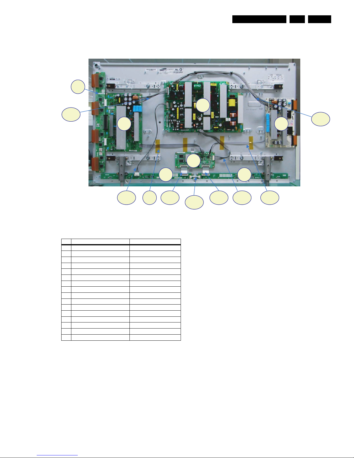
1.3.4 63” HD v4
Figure 1-14 PWB location (63” HD v4)
Table 1-6 PWB overview (50” HD w1)
G_16380_037.eps
121006
X
Y
ZG[G
\G ] ^G
_G
XW
`G
X[
X\
X^
XYG
XZ
X]G
X_
YZG
X`
YW
YXG
Y\
XX
YYG
Y[G
Y]G
No. Location Name
1 SMPS SMPS
2 LOGIC-MAIN Board Assy PWB LOGIC Main
3 X-MAIN Driving Board Assy PWB X Main
4 Y-MAIN Driving Board Assy PWB Y Main
5 LOGIC E BUFFER Board Assy PWB Buffer E
6 LOGIC F BUFFER Board Assy PWB Buffer F
7 LOGIC G BUFFER Board Assy PWB Buffer G
8 Y-BUFFER (Upper) Board Assy PWB Buffer
9 Y-BUFFER (Lower) Board Assy PWB Buffer
10 X-BUFFER (Upper) Board Assy PWB Buffer
11 X-BUFFER (Lower) Board Assy PWB Buffer
12 LOGIC + Y-MAIN FFC Cable-flat
13 LOGIC + X-MAIN FFC Cable-flat
14 LOGIC + LOGIC BUF upper (E) FFC Cable-flat
15 LOGIC + LOGIC BUF upper (F) FFC Cable-flat
16 LOGIC + LOGIC BUF upper (G) FFC Cable-flat
17 LOGIC + LOGIC BUF lower (E) FFC Cable-flat
18 LOGIC + LOGIC BUF lower (F) FFC Cable-flat
19 LOGIC + LOGIC BUF lower (G) FFC Cable-flat
20 SMPS + LOGIC MAIN Lead connector
21 SMPS + Y-MAIN Lead connector
22 SMPS + X-MAIN Lead connector
23 SMPS + LOGIC BUF upper (E) Lead connector
24 SMPS + LOGIC BUF lower (E) Lead connector
25 LOGIC BUF (E) + LOG. BUF (F) Lead connector
26 LOGIC BUF (F) + LOG. BUF (G) Lead connector

Safety Instructions, Warnings, and Notes
EN 9SDI PDP 2K6 2.
2. Safety Instructions, Warnings, and Notes
Index of this chapter:
2.1 Handling Precautions
2.2 Safety Precautions
2.3 Notes
Notes:
• Only authorised persons should perform servicing of this
module.
• When using/handling this unit, pay special attention to the
PDP Module: it should not be enforced into any other way
then next rules, warnings, and/or cautions.
• "Warning" indicates a hazard that may lead to death or
injury if the warning is ignored and the product is handled
incorrectly.
• "Caution" indicates a hazard that can lead to injury or
damage to property if the caution is ignored and the
product is handled incorrectly.
2.1 Handling Precautions
• The PDP module use high voltage that is dangerous to
humans. Before operating the PDP, always check for dust
to prevent short circuits. Be careful touching the circuit
device when power is “on”.
• The PDP module is sensitive to dust and humidity.
Therefore, assembling and disassembling must be done in
no dust place.
• The PDP module has a lot of electric devices. The service
engineer must wear equipment (for example, earth ring) to
prevent electric shock and working clothes to prevent
electrostatic.
• The PDP module use a fine pitch connector which is only
working by exactly connecting with flat cable. The operator
must pay attention to a complete connection when
connector is reconnected after repairing.
• The capacitor’s remaining voltage in the PDP module’s
circuit board temporarily remains after power is “off”.
Operator must wait for discharging of remaining voltage
during at least 1 minute.
2.2 Safety Precautions
2.2.1 Safety Precautions
• Before replacing a board, discharge forcibly the remaining
electricity from the board.
• When connecting FFC and TCPs to the module, recheck
that they are perfectly connected.
• To prevent electrical shock, be careful not to touch leads
during circuit operations.
• To prevent the Logic circuit from being damaged due to
wrong working, do not connect/disconnect signal cables
during circuit operations.
• Do thoroughly adjustment of a voltage label and voltageinsulation.
• Before reinstalling the chassis and the chassis assembly,
be sure to use all protective stuff including a nonmetal
controlling handle and the covering of partitioning type.
• Caution for design change: Do not install any additional
devices to the module, and do not change the electrical
circuit design.
• For example: Do not insert a subsidiary audio or video
connector. If you insert It, it cause danger on safety. And, if
you change the design or insert, manufacturer guarantee
will be not effect.
• If any parts of wire is overheats of damaged, replace it with
a new specified one immediately, and identify the cause of
the problem and remove the possible dangerous factors.
• Examine carefully the cable status if it is twisted or
damaged or displaced. Do not change the space between
parts and circuit board. Check the cord of AC power
preparing damage.
• Product Safety Mark: Some of electric or implement
material have special characteristics invisible that was
related on safety. In case of the parts are changed with new
one, even though the Voltage and Watt is higher than
before, the Safety and Protection function will be lost.
• The AC power always should be turned “off”, before next
repair.
• Check assembly condition of screw, parts and wire
arrangement after repairing. Check whether the material
around the parts get damaged.
2.2.2 ESD Precautions
There are parts, which are easily damaged by electrostatics
(for example Integrated Circuits, FETs, etc.) Electrostatic
damage rate of product will be reduced by the following
technics:
• Before handling semiconductor parts/assembly, must
remove positive electric by ground connection, or must
wear the antistatic wrist-belt and ring (it must be operated
after removing dust on it. It comes under precaution of
electric shock).
• After removing the assembly, lay it with the tracks on a
conductive surface to prevent charging.
• Do not use chemical stuff containing Freon. It generates
positive electric that can damage ESD sensitive devices.
• You must use a soldering device for ground-tip when
soldering or de-soldering these devices.
• You must use anti-static solder removal device. Most
removal devices do not have antistatic which can charge a
enough positive electric enough for damaging these
devices.
• Before removing the protective material from the lead of a
new device, bring the protective material into contact with
the chassis or assembly.
• When handing an unpacked device for replacement, do not
move around too much. Moving (legs on the carpet, for
example) generates enough electrostatic to damage the
device.
• Do not take a new device from the protective case until the
it is ready to be installed. Most devices have a lead, which
is easily short-circuited by conductive materials (such as
conductive foam and aluminium)
2.3 Notes
A glass plate is positioned before the plasma display. This
glass plate can be cleaned with a slightly humid cloth. If due to
circumstances there is some dirt between the glass plate and
the plasma display panel, it is recommended to do some
maintenance by a qualified service employee only.
2.3.1 Safe PDP Handling
• The work procedures shown with the “Note” indication are
important for ensuring the safety of the product and the
servicing work. Be sure to follow these instructions.
• Before starting the work, secure a sufficient working space.
• At all times, other than when adjusting and checking the
product, be sure to turn “off” the main POWER switch and
disconnect the power cable from the power source of the
display (jig or the display itself) during servicing.
• To prevent electric shock and breakage of PWBs, start the
servicing work at least 30 seconds after the main power
has been turned “off”. Especially when installing and
removing the Power Supply PWB and the SUS PWB in
which high voltages are applied, start servicing at least 2
minutes after the main power has been turned “off”.

Directions For Use
EN 10 SDI PDP 2K63.
• While the main power is “on”, do not touch any parts or
circuits other than the ones specified. The high voltage
Power Supply block within the PDP module has a floating
ground. If any connection other than the one specified is
made between the measuring equipment and the high
voltage power supply block, it can result in electric shock or
activation of the leakage-detection circuit breaker.
• When installing the PDP module in, and removing it from
the packing carton, be sure to have at least two persons
perform the work while being careful to ensure that the
flexible printed-circuit cable of the PDP module does not
get caught by the packing carton.
• When the surface of the panel comes into contact with the
cushioning materials, be sure to confirm that there is no
foreign matter on top of the cushioning materials before the
surface of the panel comes into contact with the cushioning
materials. Failure to observe this precaution may result in,
the surface of the panel being scratched by foreign matter.
• When handling the circuit PWB, be sure to remove static
electricity from your body before handling the circuit PWB.
• Be sure to handle the circuit PWB by holding the large parts
as the heat sink or transformer. Failure to observe this
precaution may result in the occurrence of an abnormality
in the soldered areas.
• Do not stack the circuit PWB. Failure to observe this
precaution may result in problems resulting from scratches
on the parts, the deformation of parts, and short-circuits
due to residual electric charge.
• Routing of the wires and fixing them in position must be
done in accordance with the original routing and fixing
configuration when servicing is completed. All the wires are
routed far away from the areas that become hot (such as
the heat sink). These wires are fixed in position with the
wire clamps so that the wires do not move, thereby
ensuring that they are not damaged and their materials do
not deteriorate over long periods of time. Therefore, route
the cables and fix the cables to the original position and
states using the wire clamps.
• Perform a safety check when servicing is completed. Verify
that the peripherals of the serviced points have not
undergone any deterioration during servicing. Also verify
that the screws, parts and cables removed for servicing
purposes have all been returned to their proper locations in
accordance with the original
3. Directions For Use
Not applicable.

Mechanical Instructions
EN 11SDI PDP 2K6 4.
4. Mechanical Instructions
Index of this chapter:
4.1 Dis-assembling / Re-assembling
4.1.1 Flexible Printed Circuit of Y-Buffer (Upper and Lower)
4.1.2 Flat Cable Connector of X-main Board
4.1.3 FFC and TCP from Connector
4.1.4 Exchange of LBE and LBF board - 42” SD v5
4.1.5 Exchange of LBE and LBF board - 42” HD w1
4.1.6 Exchange of LBE, LBF and LBG board - 50” HD w1
4.1.7 Exchange of LB-E, LB-F and LB-G board - 63” HD v4
4.1.8 Exchange YB and YM board - 42” SD v5
4.1.9 Exchange YB and YM board - 42” HD w1
4.1.10 Exchange YBU, YBL and YM board - 50” HD w1
4.1.11 Exchange YBU, YBL and YM board - 63” HD v4
4.1 Dis-assembling / Re-assembling
4.1.1 Flexible Printed Circuit of Y-Buffer (Upper and Lower)
• Dis-assembly: Pull out the FPC from the connector by
holding the lead of the FPC with both hands.
• Re-assembly: Push the lead of FPC with same force on
both sides into the connector.
Note: Be careful not to damage the connector pin during
connecting.
Figure 4-1 Dis-assembly FPC of Y-buffer
Figure 4-2 Re-assembly FPC of Y-buffer
G_16380_012.eps
190606
G_16380_013.eps
190606

Mechanical Instructions
EN 12 SDI PDP 2K64.
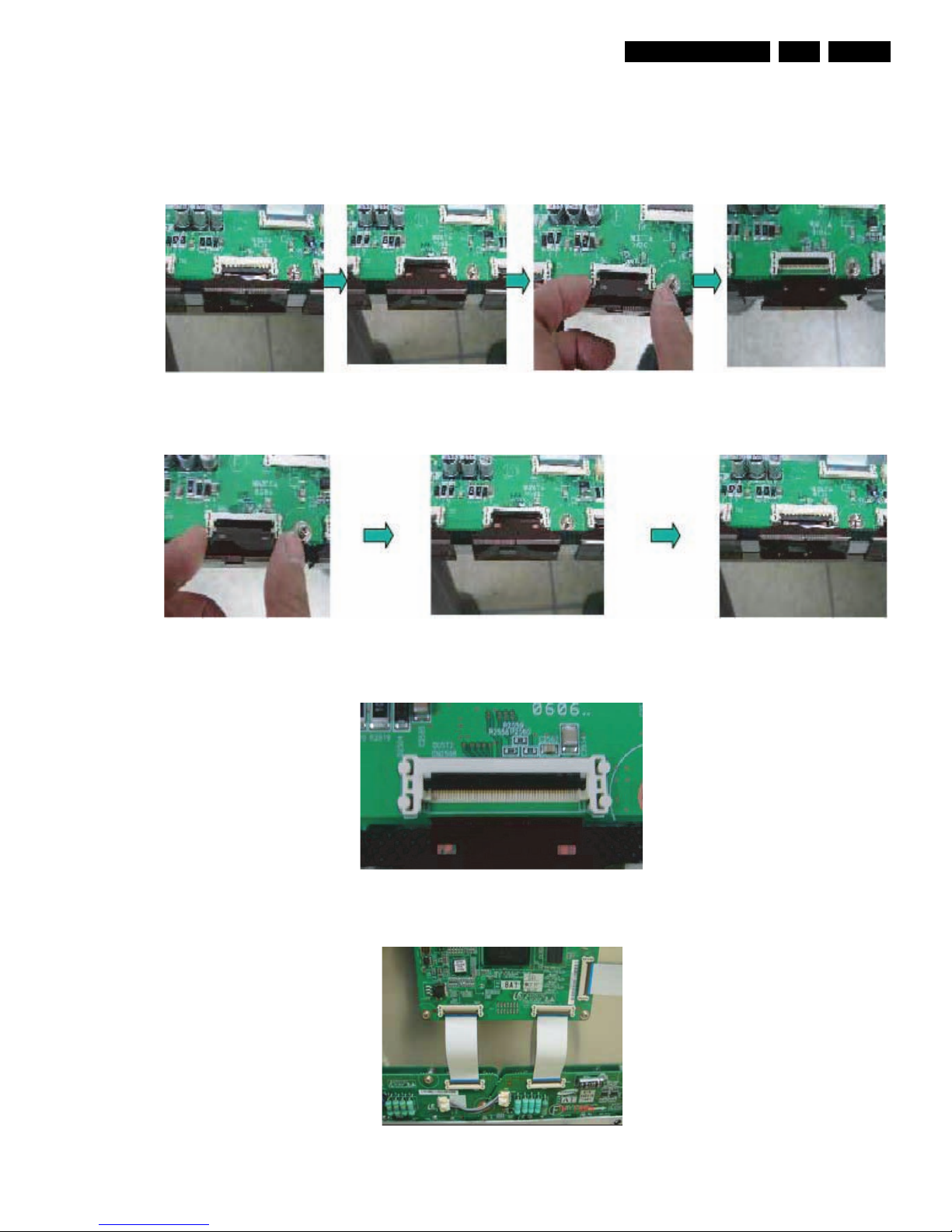
4.1.2 Flat Cable Connector of X-main Board
• Dis-assembly:
1. Pull out the clamp of connector.
2. Pull Flat cable out press down lightly.
3. Turn the Flat Cable reversely.
• Re-assembly: Put the Flat Cable into the connector press
down lightly until you hear a “Click“.
Figure 4-3 Dis-assembly FCC of X-main board
Figure 4-4 Re-assembly FCC of X-main board
G_16380_014.eps
190606
G_16380_015.eps
190606
Mechanical Instructions
EN 13SDI PDP 2K6 4.
4.1.3 FFC and TCP from Connector
• Dis-assembling of TCP:
1. Open the clamp carefully.
2. Pull the TCP out from its connector.
• Re-assembling of TCP:
1. Put the TCP into the connector carefully
2. Close the clamp completely, until you hear a “Click”.
Notes:
• Checking whether the foreign material is on the connector
inside before assembling of TCP.
• Be careful, do not damage the board by ESD during
handling of TCP.
Figure 4-5 Dis-assembly of TCP
Figure 4-6 Re-assembly of TCP
Figure 4-7 Mis-assembly of TCP
Figure 4-8 Dis- and re-assembly of FFC
G_16380_016.eps
190606
G_16380_017.eps
190606
G_16380_018.eps
190606
G_16380_019.eps
190606
Mechanical Instructions
EN 14 SDI PDP 2K64.
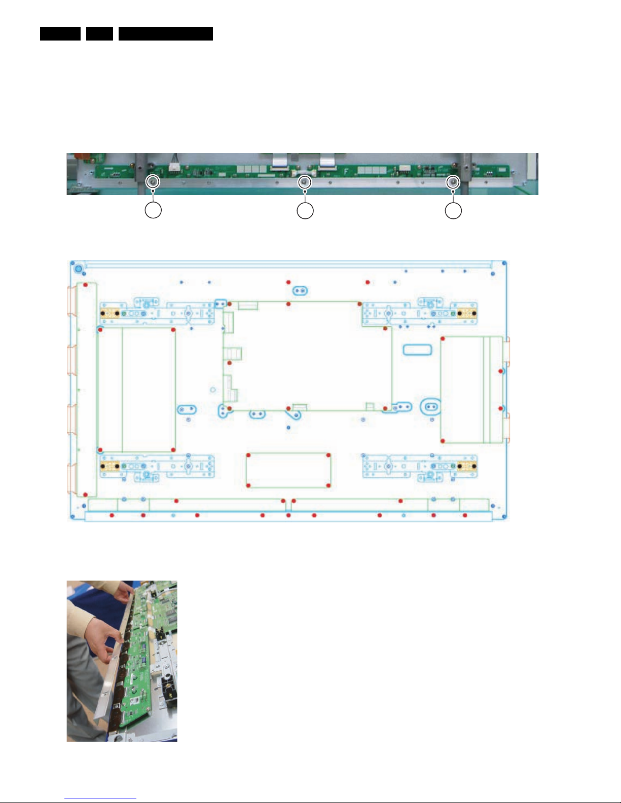
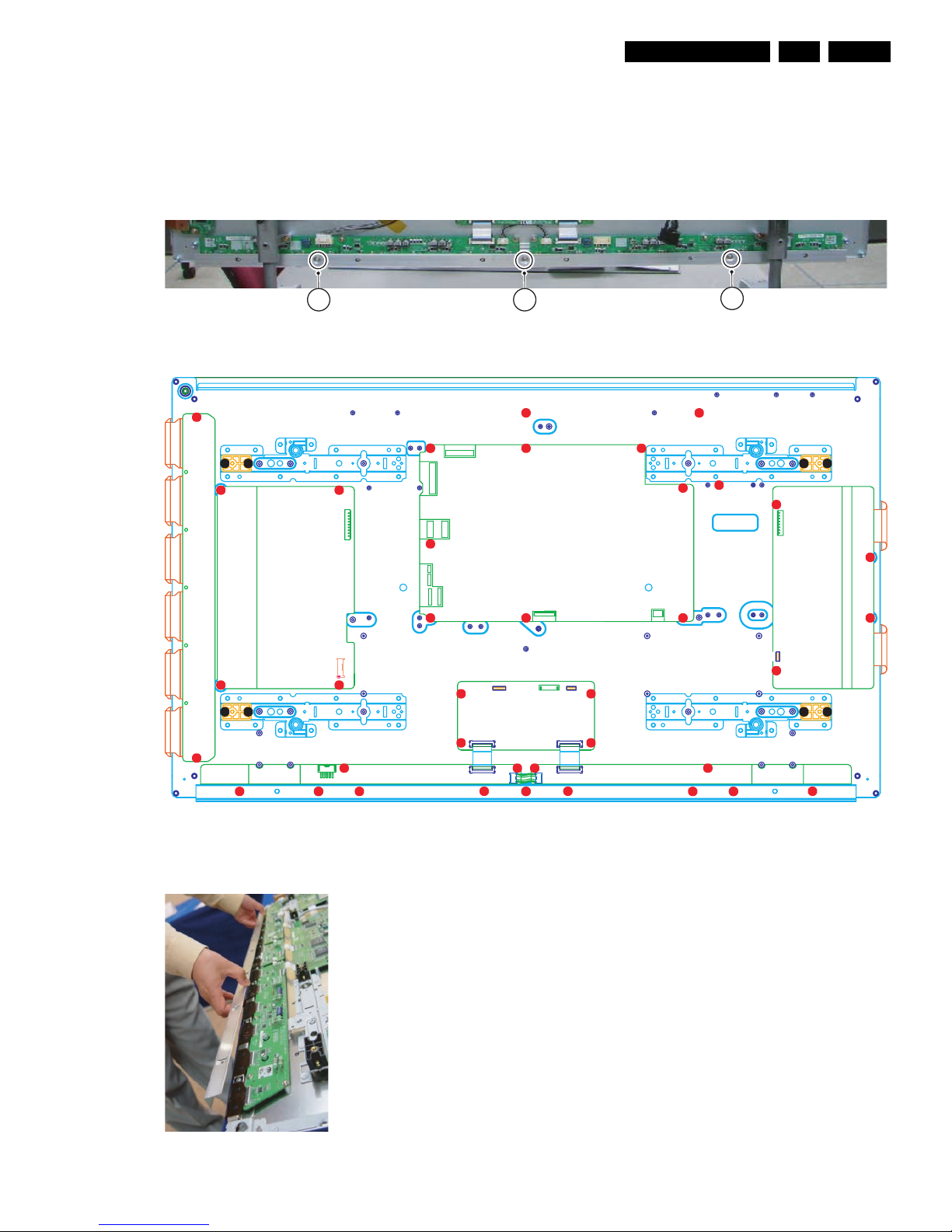
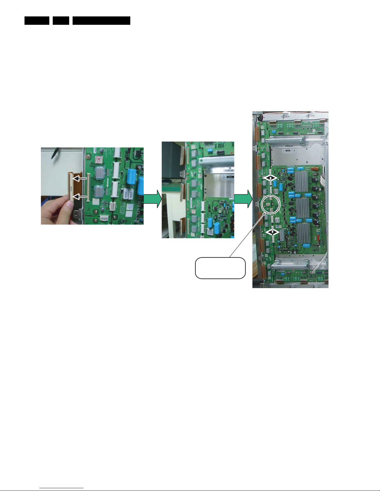
4.1.4 Exchange of LBE and LBF board - 42” SD v5
1. Remove the screws in order of 1-3-2 from the heatsink and
remove the heatsink (“Photos 1 & 3”)
2. Remove the TPC, FFC, and the power cable from the
connectors.
3. Remove all the screws from the defective board (“Photo
2”).
4. Remove the defective board.
5. Place the new board and screw it tight.
6. Clean the connectors.
7. Re-connect the TCP, FFC, and the power cable to the
connectors.
8. Re-assemble the TCP heat sink. Use the screw mounting
order 2-3-1.
Caution: If you screw too tight, it is possible to damage the
Driver IC of the TCP.
Figure 4-9 Photo 1 - Heatsink 42” SD v5
Figure 4-10 Photo 2 - Exchange of LBE and LBF board 42” SD v5
Figure 4-11 Photo 3 - Heat sink removal
G_16380_020.eps
160606
3
2
1
G_16380_021.eps
160606
G_16380_022.eps
160606
Mechanical Instructions
EN 15SDI PDP 2K6 4.
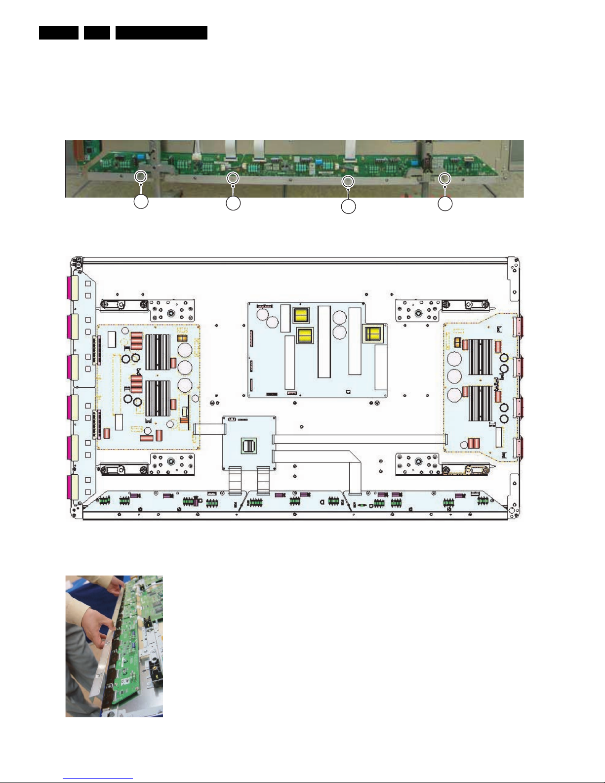
4.1.5 Exchange of LBE and LBF board - 42” HD w1
1. Remove the screws in order of 1-3-2 from the heatsink and
remove the heatsink (“Photos 1 & 3”).
2. Remove the TPC, FFC, and power cable from the
connectors.
3. Remove all the screws from the defective board.
4. Remove the defective board.
5. Place the new board and then screw tightly.
6. Clean the connectors.
7. Re-connect the TCP, FFC, and power cable to the
connectors.
8. Re-assemble the TCP heat sink. Use the screw mounting
order 2-1-3.
Caution: If you screw too tight, it is possible to damage the
Driver IC of the TCP.
Figure 4-12 Photo 1 - Heatsink 42” HD w1
Figure 4-13 Photo 2 - Exchange of LBE, LBF board 42” HD w1
Figure 4-14 Photo 3 - Heat sink removal
1
3
2
G_16380_027.eps
160606
G_16380_024.eps
160606
G_16380_022.eps
160606
Mechanical Instructions
EN 16 SDI PDP 2K64.
4.1.6 Exchange of LBE, LBF and LBG board - 50” HD w1
1. Remove the screws in order of 2-3-1-4 from the heatsink
and remove the heatsink (“Photo 3”).
2. Remove the TPC, FFC, and power cable from the
connectors.
3. Remove all the screws from the defective board.
4. Remove the defective board.
5. Replace the new board and then screw tightly.
6. Clean the connectors.
7. Re-connect the TCP, FFC, and power cable to the
connectors.
8. Re-assemble the TCP heat sink. Use the same screw
mounting order as described above
Caution: If you screw too tight, it is possible to damage the
Driver IC of the TCP.
Figure 4-15 Photo 1 - Heatsink 50” HD w1
Figure 4-16 Photo 2 - Exchange of LBE, LBF, LBG board 50” HD w1
Figure 4-17 Photo 3 - Heat sink removal
G_16380_023.eps
160606
4
3
2
1
G_16380_026.eps
160606
G_16380_022.eps
160606

Mechanical Instructions
EN 17SDI PDP 2K6 4.
4.1.7 Exchange of LB-E, LB-F and LB-G board - 63” HD v4
1. Refer to the Service Manual of the set to strip it so far, you
have access to the Logic Buffer board that you need to
replace.
2. For the lower LB-E, remove brackets [1] and [2]; for the
lower LB-G, remove brackets [3] and [4]. For both LB-F’s
and the upper LB-E and LB-G you do not need to remove
these brackets.
Note: The following description is correct for the lower
LBG; the replacement procedure of the other LB’s is
similar.
3. Remove the fixation screws [5] from the TPC heatsinks of
the defective board.
4. Unplug the TPC, FFC, and power cable(s) from the
connectors [6].
5. Remove the fixation screws from the defective board [7].
6. Remove the defective board.
7. Replace the new board and then screw tightly.
8. Clean the connectors.
9. Re-connect the TCP, FFC, and power cable to the
connectors.
10. Re-assemble the TCP heat sinks. Slide the heatsink
against strip [8] before you tighten it.
Figure 4-18 Brackets 63” HD v4
Figure 4-19 Exchange of lower LB-G board 63” HD v4
G_16380_038.eps
131006
2
1
4
3
G_16380_039.eps
131006
7
6
5 5
6
7
7
7
7
8
Mechanical Instructions
EN 18 SDI PDP 2K64.
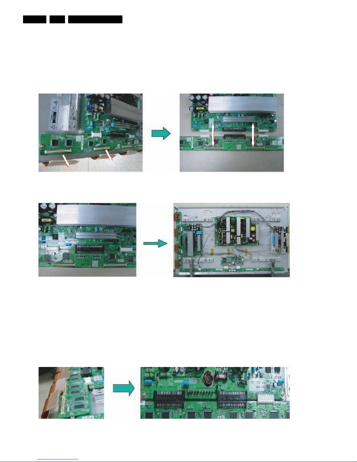
4.1.8 Exchange YB and YM board - 42” SD v5
1. Unplug all of the FPC connectors of Y-Buffer. See “Photo
1”.
2. Unplug connectors CN5001 and CN5008 from YMain. See “Photo 2”.
3. Loosen all the screws of Y-Buffer and Y-Main. See “Photo
3”.
4. Remove the board from the chassis.
5. Unplug connectors CN5003, CN5004 and CN5005
between Y-Buffer and Y-Main.
6. Remove Y-Buffer from Y-main.
7. Replace the defective board.
8. Re-assemble Y-Buffer and Y-Main.
9. Plug in connectors CN5003, CN5004 and CN5005
between Y-Buffer and Y-Main. See “Photo 4”.
10. Arrange the boards on the chassis and tighten them.
11. Connect the FPC connectors. See “Photo 5”.
12. Supply the electric power to the module and then check the
waveform of the board.
13. Turn “off” the power after the waveform is adjusted.
Figure 4-20 Photo 1 and 2: Dis-assembly of YB and YM - 42” SD v5
Figure 4-21 Photo 3 and 4: Re-assembly of YB and YM - 42” SD v5
4.1.9 Exchange YB and YM board - 42” HD w1
1. Unplug all of the FPC connectors of Y-Buffer. See “Photo
1”.
2. Loosen all the screws of Y-Buffer and Y-Main. See “Photo
3”.
3. Remove the board from the chassis.
4. Unplug connectors CN5004, CN5011 and CN5012
between Y-Buffer and Y-Main.
5. Remove Y-Buffer from Y-main.
6. Replace the defective board.
7. Re-assemble Y-Buffer and Y-Main.
8. Plug in connectors CN5004, CN5011 and CN5012
between Y-Buffer and Y-Main. See “Photo 4”.
9. Arrange the boards on the chassis and tighten them.
10. Connect the FPC connectors.
11. Supply the electric power to the module and then check the
waveform of the board.
12. Turn “off” the power after the waveform is adjusted.
Figure 4-22 Photo 1 and 2: Dis-assembly of YBU, YBL, and YM - 42” HD w1
G_16380_030.eps
190606
G_16380_031.eps
190606
G_16380_032.eps
190606
Mechanical Instructions
EN 19SDI PDP 2K6 4.
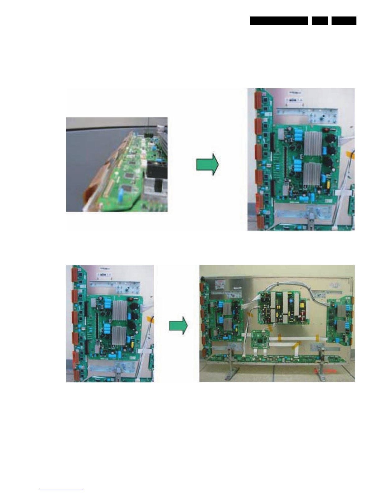
4.1.10 Exchange YBU, YBL and YM board - 50” HD w1
1. Unplug all of the FPC connectors of YBU (Y-Buffer upper)
and YBL (Y-Buffer lower). See “Photo 1”.
2. Unplug the connector CN5412 between YBU and YBL.
3. Loosen all the screws of YBU, YBL, and Y-Main.
4. Remove the board from the chassis.
5. Remove the YBL and YBU from Y-main.
6. Replace the defective board.
7. Re-assemble the YBU and YBL to the Y-Main.
8. Plug in connector CN5412 between YBU and YBL.
9. Arrange the board on the chassis and then screw to fix.
10. Connect the FPCs.
11. Supply the electric power to the module and then check the
waveform of the board.
12. Turn “off” the power after the waveform is adjusted.
Figure 4-23 Photo 1 and 2: Dis-assembly of YBU, YBL, and YM - 50” HD w1
Figure 4-24 Photo 3 and 4: Re-assembly of YBU, YBL, and YM - 50” HD w1
G_16380_033.eps
190606
G_16380_034.eps
190606
Mechanical Instructions
EN 20 SDI PDP 2K64.
4.1.11 Exchange YBU, YBL and YM board - 63” HD v4
1. Unplug power connector CN5010 and signal connector
CN5002 from Y-Main. See “Photo 1”.
2. Unplug all FPC connectors of YBU (Y-Buffer upper) and
YBL (Y-Buffer lower). See “Photo 1”.
3. Open the connectors CN5001/CN5406 between YM and
YBU, and CN5000/CN5506 between YM and YBL.
4. Loosen all the screws of YBU, YBL, and Y-Main.
5. Remove the boards from the chassis.
6. Open the connectors CN5410/CN5510 between YBU and
YBL.
7. Separate the YBL and YBU from Y-main.
8. Replace the defective board.
9. Re-assemble the YBU and YBL to the Y-Main.
10. Plug in the connectors between YBU, YBL and YM.
11. Arrange the board on the chassis and then screw to fix.
12. Reconnect the FPCs.
13. Supply the electric power to the module and then check the
waveform of the board.
14. Turn “OFF” the power after the waveform is adjusted.
Figure 4-25 Photo 1: Dis-assembly of YBU, YBL, and YM - 63” HD v4
G_16380_042.eps
161006
Make sure you open these
connectors before you
separate the boards !
Service Modes, Error Codes, and Fault Finding
EN 21SDI PDP 2K6 5.
5. Service Modes, Error Codes, and Fault Finding
Index of this chapter:
5.1 Repair Tools
5.1.1 ComPair
5.1.2 Other Service Tools
5.2 Fault Finding
5.2.1 Possible Scenarios
5.2.2 Faulty Power Supply
5.2.3 No Display
5.2.4 Abnormal display
5.2.5 Horizontal line or block open
5.2.6 Address open
5.2.7 Address short
5.2.8 Criteria for Panel Replacement, due to Defective Panel
Cells
5.2.9 Overview
5.3 Defect Description Form
5.1 Repair Tools
5.1.1 ComPair
For the v5 and w1 models, it will be possible to generate test
patterns with ComPair. The ComPair interface must be
connected to the Logic Board with the special interconnection
cable (see table below for the order code).
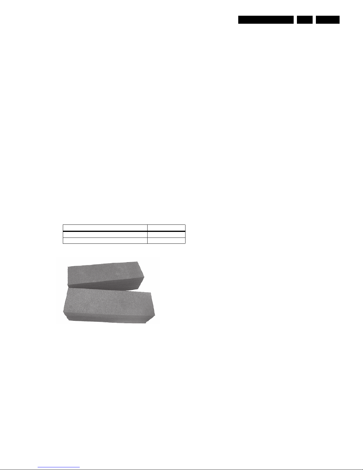
5.1.2 Other Service Tools
Table 5-1 Overview Service tools
Figure 5-1 Foam buffers
Service Tools
Order Code
ComPair / SDI interconnection cable 3122 785 90800
Foam buffers (2 pcs.) 3122 785 90581
G_16380_029.eps
160606

Service Modes, Error Codes, and Fault Finding
EN 22 SDI PDP 2K65.
5.2 Fault Finding
5.2.1 Possible Scenarios
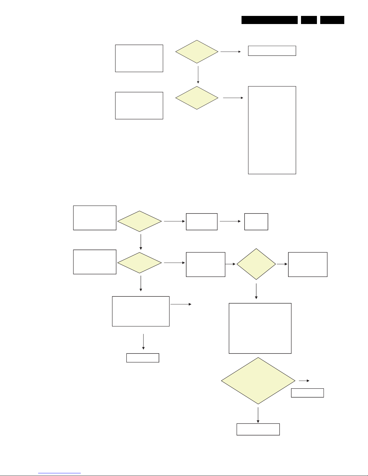
Figure 5-2 Which repair scenario?
Chassis ?
Repair Scenario
42” SD v5
First check complete TV set.
Fault Symptom?
Check if LVDS from
SSB board is OK.
Use LVDS Tool when possible.
Output of SSB
is OK?
SDI repair Scenario.
Fault finding: Display fault.
Repair Philips application.
See chassis related Service Manuals
No
Power Supply
is working ?
Go to
“Power Supply Check”
& repair scenario
with Philips application
or PDP as stand alone check.
No
Repair Scenario
50” HD w1
Power supply is not working.
No voltage output.
G_16380_120.eps
161006
LC4.41E AB
BJ2.4U PA
Repair Scenario
63” HD v4
BJ3.0U PA
Repair Scenario
42” HD w1
BJ2.5U PA
BJ2.4U PA
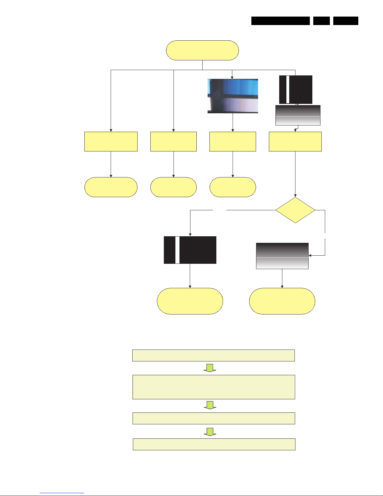
Service Modes, Error Codes, and Fault Finding
EN 23SDI PDP 2K6 5.
Figure 5-3 Fault symptom overview (complete TV set)
Figure 5-4 Repair scenario stand alone panels
No Voltage output
Operating Voltages don´t exist
Operating Voltages exist,
but No Display
Abnormal Display, not
open or short Lines
Some horizontal or Vertical
Lines don´t exist on the
Display.
Sustain open
First check complete TV set.
Fault Symptom?
Go to
“Power Supply Check”
(version dependent)
Go to
“No Display”
Go to the
“Abnormal Display”
Is related to X-Main, Y-Main
and Y-buffer.
Go to
“Sustain Open / Short”
Horizontal or
Vertical Lines?
Vertical
Is related to Logic adress Buffer.
Go to
“Address Open / Short”
Horizontal
flowchart
flowchart
flowchart
flowchart
flowchart
G_16380_056.eps
160606
XUGjGGGGGGG G
YUGjGGGsGGGG[YˉzkG\aGGslkGYWWWG
GGGGGG[YˉokGXaGslkGYWXXG
GGGGGG\WˉokGXaGslkGYWWYG
GGGGGG]ZˉokG[aGGslkGYWWYG G
ZUGjVGGG
GGG
G
[UGjGGGGGG
G_16380_122.eps
161006
Service Modes, Error Codes, and Fault Finding
EN 24 SDI PDP 2K65.
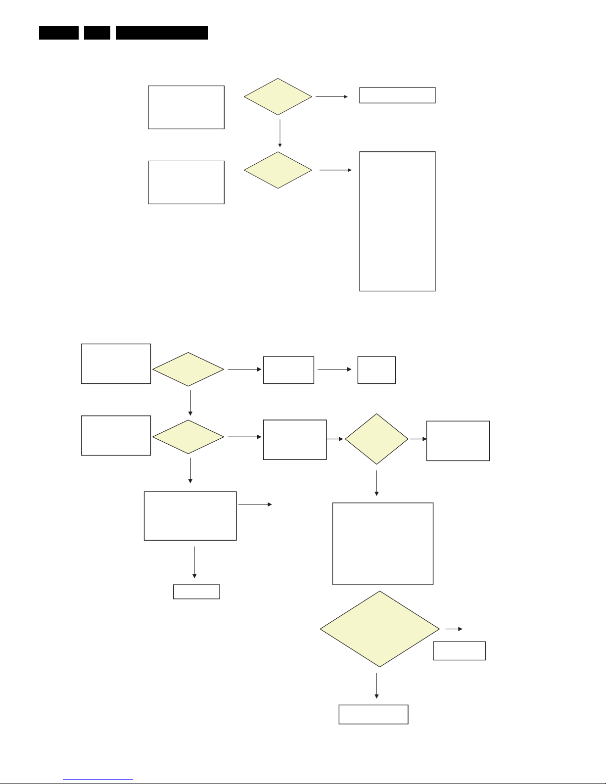
5.2.2 Faulty Power Supply
Figure 5-5 Power Supply Check for 42” SD v5 models 1/2
Figure 5-6 Power Supply Check for 42” SD v5 models 2/2
AC Input
Check CN8001/2pin
Connect [220V ac]
Reconnect it
N
NO
YES
D5V: 5V Check
Vs: 207V Check
Va: 65V Check
Vset: 201V Check
Vscan: -190V Check
Ve:110V Check
Vcc: 15V Check
D3V3: 3.3V Check
5Vstandby: 5.2V Check
Fuse
8001/8002/8005/8007
Replace SMPS
SMPS Voltage check
SMPS
LED 8001,8002
Green
Check
NO
O
1
G_16380_123.eps
190606
SMPS
On/OFF Relay
(RLY 8001, 8002
Acts?
LED (Green)
N
NO
8001
,
8002 off
SMPS
SMPS
Check Protection,
YES
NO
Open CN 8001
Until LED 8004 OFF,
Then Reset SMPS
Check
Vs_
on
LED 8004(RED) is
OFF?
Replace
NO
Under voltage
Checkin
g,
repeat
If LED8004 is ON
YES
YES
Vs, Va, Vset, Vscan, Ve
Check output voltage
NO
Open these connector
One by One
- CN8002, X-Main check
- CN8003, Y-Main check
- CN8005/CN8006 Buffer check
Turn off Relay SW
Re
p
lace
Replace SMPS
Vs, Va, Vset, Vscan, Ve
Check output voltage
NO
YES
Go to 5.2.3 No Display
O
1
O
1
G_16380_123a.eps
190606
=>
Service Modes, Error Codes, and Fault Finding
EN 25SDI PDP 2K6 5.
Figure 5-7 Power Supply Check for 42” HD w1 models 1/2
Figure 5-8 Power Supply Check for 42” HD w1 models 2/2
AC Input
Connect [ 220Vac]
Check CN8001/2pin
Reconnect it
NO
YES
Replace SMPS
Fuse
8001/8002/8005/8007
5Vstandby: 5.2V Check
D3V3: 3.3V Check
Vcc:15V Check
Ve:110V Check
Vscan: -190V Check
Vset: 190V Check
Va: 65V Check
Vs: 195V Check
D5V: 5V Check
SMPS Voltage check
SMPS
Green
LED 8001,8002
Check
NO
O
1
G_16380_124.eps
190606
SMPS
On/OFF Relay
(RLY 8001, 8002
Acts?
LED (Green)
8001
,
8002 off
NO
YES
SMPS
YES
Check output voltage
Vs, Va, Vset, Vscan, Ve
NO
Replace SMPS
Turn off Relay SW
Check output voltage
Vs, Va, Vset, Vscan
NO
YES
Replace SMPS
,Ve
- CN8003, Y-Main check
- CN8005/CN8006 Buffer check
Open these connectors
One by One
- CN8002, X-Main check
Check
Vs_
on
Open CN 8001
Until LED 8004 OFF,
Then Reset SMPS
NO
OFF?
Check Protection,
LED 8004(RED) is
SMPS
Replace
NO
Checking, repeat
If LED 8004 is ON
Under voltage
YES
->
O
1
O
1
G_16380_124a.eps
190606
Go to 5.2.3 No Display
 Loading...