

Philips RX1214B350Y Datasheet

DISCRETE SEMICONDUCTORS
DATA SH EET
RX1214B350Y
NPN microwave power transistor
Product specification
Superseded data of November 1994
1997 Feb 18
Philips Semiconductors Product specification
NPN microwave power transistor RX1214B350Y
FEATURES
• Suitable for short and medium
pulse applications up to 1 ms/10%
• Internal input prematching
networks allow an easier design of
circuits
• Diffused emitter ballasting resistors
improve ruggedness
• Interdigitated emitter-base
structure provides high emitter
efficiency
• Gold metallization with barrier
realizes very stable characteristics
and excellent lifetime
• Multicell geometry improves power
sharing and reduces thermal
resistance.
APPLICATIONS
Common base, class C, broadband,
pulsed power amplifiers for L-Band
radar applications in the
1.2 to 1.4 GHz band. Also suitable for
medium pulse, heavy duty operation
within this band.
DESCRIPTION
QUICK REFERENCE DATA
Microwave performance up to T
=25°C in a common base class C
mb
broadband amplifier.
MODE OF
OPERATION
Class C t
CONDITIONS
= 130 µs;
p
f
(GHz)
1.2 to 1.4 50 280 ≥7 ≥40
δ =6%
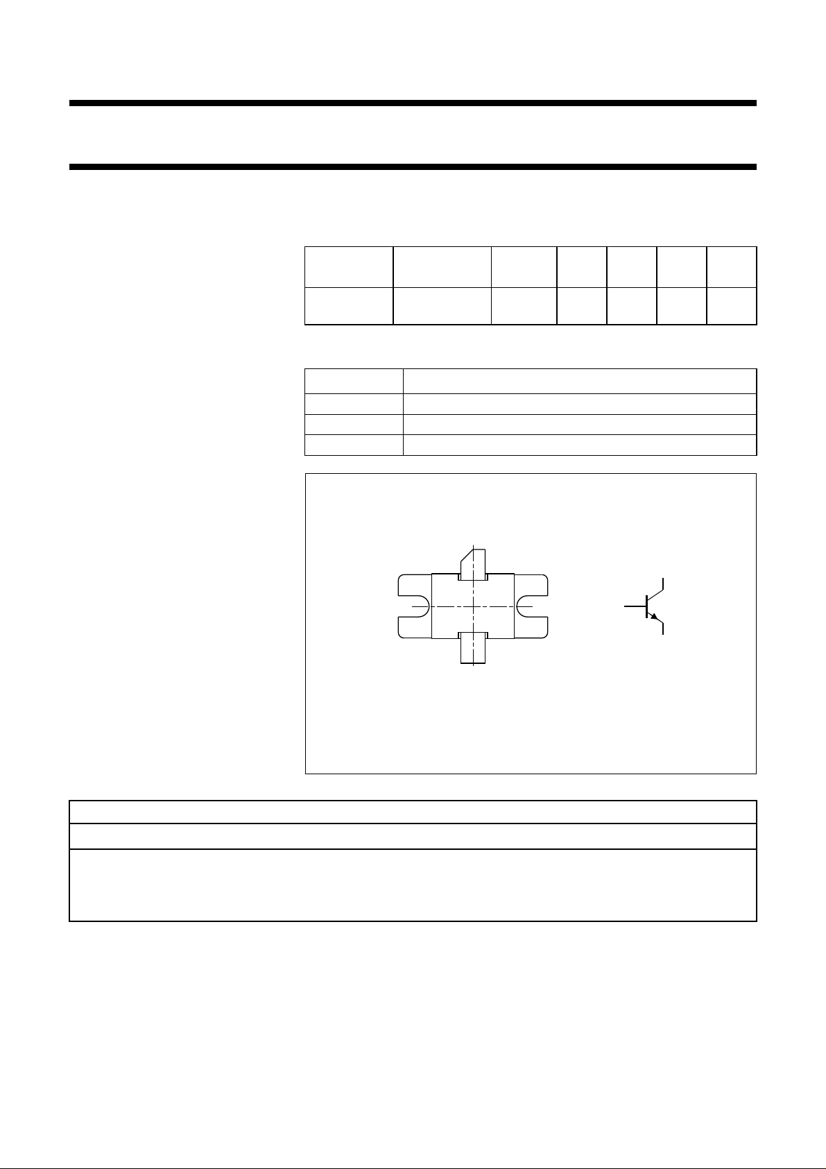
PINNING - SOT439A
PIN DESCRIPTION
1 collector
2 emitter
3 base connected to flange
handbook, 4 columns
Top view
1
2
V
CC
(V)
33
MAM045
P
(W)
b
G
L
(dB)
c
e
η
p
C
(%)
NPN silicon planar epitaxial
microwave power transistor in a
SOT439A metal ceramic flange
package with base connected to
Fig.1 Simplified outline and symbol.
flange.
WARNING
Product and environmental safety - toxic materials
This product contains beryllium oxide. The product is entirely safe provided that the BeO disc is not damaged.
All persons who handle, use or dispose of this product should be aware of its nature and of the necessary safety
precautions. After use, dispose of as chemical or special waste according to the regulations applying at the location of
the user. It must never be thrown out with the general or domestic waste.
1997 Feb 18 2
Philips Semiconductors Product specification
NPN microwave power transistor RX1214B350Y
LIMITING VALUES
In accordance with the Absolute Maximum System (IEC 134).
SYMBOL PARAMETER CONDITIONS MIN. MAX. UNIT
V
CBO
V
CEO
V
CES
V
EBO
I
C
P
tot
T
stg
T
j
T
sld
Note
1. Up to 0.2 mm from ceramic.
collector-base voltage open emitter − 65 V
collector-emitter voltage open base − 20 V
collector-emitter voltage RBE=0Ω−65 V
emitter-base voltage open collector − 3V
collector current (DC) tp≤ 130 µs; δ≤6% − 25 A
total power dissipation Tmb<75°C;
− 750 W
tp≤ 30 µs; δ≤1%
storage temperature −65 200 °C
operating junction temperature − 200 °C
soldering temperature t ≤ 10 s; note 1 − 235 °C
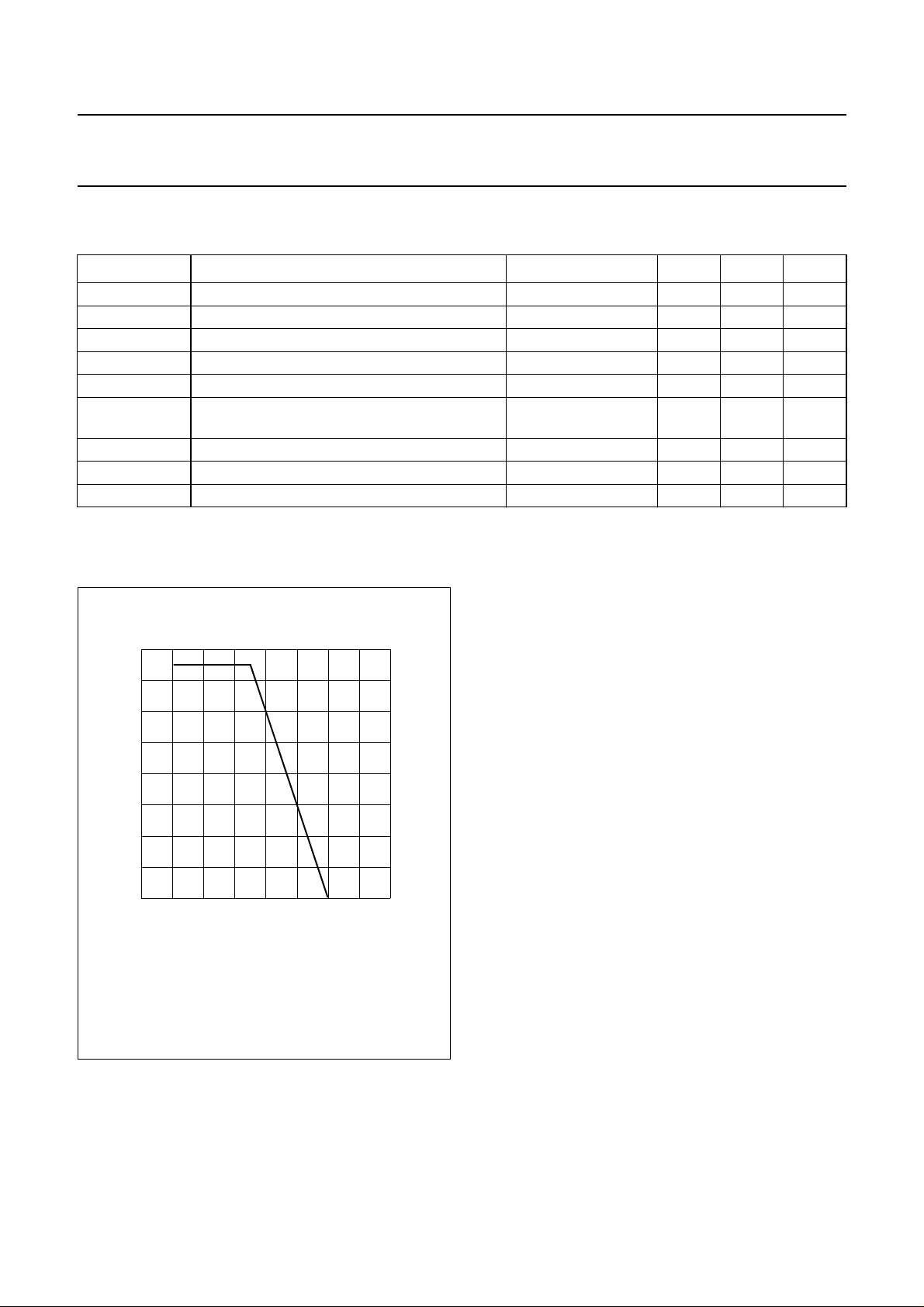
200
T
amb
MGA259
(
800
handbook, halfpage
P
tot
(W)
600
400
200
0
–100 0 100 300
P
= 750W; tp≤ 30 µs; δ≤1%.
tot max
Fig.2 Maximum power dissipation derating as a
function of mounting base temperature.
o
C)
1997 Feb 18 3

Philips Semiconductors Product specification
NPN microwave power transistor RX1214B350Y
THERMAL CHARACTERISTICS
SYMBOL PARAMETER CONDITIONS MAX. UNIT
R
th j-mb
R
th mb-h
Z
th j-h
Notes
1. See
“Mounting recommendations in the General part of handbook SC19a”
2. Equivalent thermal impedance under pulsed microwave operating conditions.
CHARACTERISTICS
=25°C unless otherwise specified.
T
mb
SYMBOL PARAMETER CONDITIONS MAX. UNIT
I
CBO
I
EBO
thermal resistance from junction to mounting base Tj= 120 °C 1.2 K/W
thermal resistance from mounting base to heatsink note 1 0.2 K/W
thermal impedance from junction to heatsink tp= 130 µs; δ = 6%;
0.17 K/W
Tj=110°C; notes 1 and 2
.
collector cut-off current VCB=50V; IE= 0 30 mA
emitter cut-off current VEB= 1.5 V; IC=0 3 mA
APPLICATION INFORMATION
Microwave performance up to T
MODE OF
OPERATION
Class C t
p
CONDITIONS
= 130 µs; δ = 6%; note 2 1.2 to 1.4 50 280 ≥7;
=25°C in a common base test circuit as shown in Fig.3.
mb
V
f
(GHz)
CC
(V)
note 1
P
(W)
L
G
(dB)
typ. 8
Notes
1. V
during pulse.
CC
2. Operating conditions and performances for other pulse formats can be made available on request.
p
η
C
(%)
≥40;
typ. 44
1997 Feb 18 4
 Loading...